DESIGN OF A THERMAL OPERATIONAL AMPLIFIER: THERMICS APPLIED TO HEAT SIGNAL CONTROL
by
ROGER LEE MCCARTHY
A.B., University of Michigan (1972)
B.S.E. (M.E.) University of Michigan (1972)
S.M., Massachusetts Institute of Technology (1973)
Mech. E., Massachusetts Institute of Technology (1975)
SUBMITTED IN PARTIAL FULFILLMENT OF THE REQUIREMENTS FOR THE
DEGREE OF DOCTOR OF PHILOSOPHY
at the
MASSACHUSETTS INSTITUTE OF TECHNOLOGY March 1, 1977
Signature of Author... ...
Departnt / E MecIan~ cal Eng ~aeeing, March 1, 1977 Certified by...
7
A; _hesis Supervisor
/I
Accepted by... ... Chairman, Department Committee on Graduate Students
ARCHIVES
DESIGN OF A THERMAL OPERATIONAL AMPLIFIER: THERMICS APPLIED TO HEAT SIGNAL CONTROL.
by
ROGER LEE MCCARTHY
Submitted to the Department of Mechanical Engineering on March 1, 1977 in partial fulfillment of the requirements for
the Degree of Doctor of Philosophy. ABSTRACT
A thermal differential operational amplifier was developed through an experimentally verified analysis of design parameters. In general, an operational amplifier (or Op-Amp) is a device which ampli-fies a signal by a constant factor, called the amplifier's gain. A thermal differential Op-Amp takes a small temperature difference be-tween its negative and positive inputs and produces a much larger output temperature difference. Conceived as the building block for linear thermal logic, or thermics, the amplifier is an active control element operating totally in the thermal-energy domain, using temperatures for input and output, and heat for power. A detailed seventh-order analy-tical model of the amplifier used physical dimensions and material pro-perties to predict step-input response (open and closed loop). Predic-tions agreed with open-and-closed loop dynamic-response tests performed on experimental prototypes. The selection of physical dimensions to produce desired dynamic behavior was accomplished with an optimal-de-sign technique.
The amplifier was constructed from two effort (temperature) controlled resistors (ECR) which were series connected in a push-pull configuration. The trade of gain for range is identified and expressions for each constructed in terms of thermal-resistor parameters. The proto-type utilized planar-film ECR's, in which the level of a conducting fluid in an air gap varies thermal resistance. The fluid level is modulated by the temperature difference between negative and positive sensors, which creates an output temperature proportional to the input temperature difference.
When tested open loop, the ratio of amplifier output to input had a constant value of twenty over the amplifier's output operating range, typically + 300F from a reference. Configured closed loop as an effort follower the 90% rise time was less than three minutes. Closed loop operation proved that an amplifier building block for analog ther-mic circuits was feasible.
Thesis Supervisor: B. Shawn Buckley
Title: Associate Professor of Mechanical Engineering
-2-ACKNOWLEDGMENTS
First, and foremost, the author must express his sincere gratitude to his friend and advisor, Professor B. Shawn Buckley. Space does not permit narration of all the advice, encouragement, insight, and help extended to the author; suffice it to say this is not a
cus-tomary acknowledgment, but a statement of truly heartfelt appreciation.
Secondly, the author must acknowledge the significant con-tribution made to this effort, and to his life, by his friend David W. Mercaldi, who had the patience and the misfortune to listen to many of the author's bad ideas, and all of his rude remarks, so that you, the reader, were spared.
The other members of the committee; Prof. Peter Griffith, Prof. Henry M. Paynter, and Prof. David G. Wilson, were universally positive in their attitude, encouraging, and extremely helpful to the author, for which he is deeply grateful.
Cliflex Bellows Corp. of Boston practically donated 8 bellows to the author that made a working prototype possible.
Leslie Regan's undying patience and late hours typing this manuscript deserves special mention.
Finally, to all who made the atmosphere at Tech what it was; Neville, Lampe, Jeff, Tom, Bob, Anna, Woodie, Dave, Rich, Joe, Omezie, Sandy, Fred, Jim, Mark, Jerry, John, and even Steve, I wish to say thank you, in my weaker moments I'll miss you all.
This work was made possible through the generous support of the National Science Foundation, the Dupont Science and Engineering
Grant, and the Energy Research and Development Agency.
-4-Dedication:
To my parents,
William H. and Eloise E. McCarthy
TABLE OF CONTENTS Page Title Page... 1 Abstract ... 2 Acknowledgments... 3 Dedication... 5 Table of Contents... 6 List of Tables ... 10 List of Figures...11... ... 11 CHAPTER 1: INTRODUCTION ... 14
Section 1-1: Brief chapter summary... 14
Section 1-2: Description and justification... 15
Section 1-3: Brief history of active thermal control.... 20
CHAPTER 2: THEORY OF AMPLIFIER OPERATION... 26
Section 2-1: Brief chapter summary... 26
Section 2-2: Definition and description of ideal operational amplifier... 27
Section 2-3: Amplifier nonidealities... 30
Section 2-4: Use of the amplifier in operational circuits ... 37
CHAPTER 3: THE THERMAL OPERATIONAL AMPLIFIER... 47
Section 3-1: Brief chapter summary... 47
Section 3-2: Description of the thermal operational amplifier... 49
Section 3-3: Linearized amplifier description... 54
Section 3-4: Gain parameters ... 61
Section 3-5: Temperature modulated resistors... 68
Part 3-5A: General description of thermal resistors ... 68
Part 3-5B: Planar thermal resistors ... 70
Part 3-5C: The film resistor... 75
Part 3-5D: Geometry of the film resistor... 77
Part 3-5E: Analysis of the film ECR... 83
-6-Page
Section 3-6: Amplifier construction from two
film ECR's... 90
Part 3-6A: Topology of the two film ECR amplifier ... 90
Part 3-6B: Compensation of ECR nonlinearity ... 94
CHAPTER 4: AMPLIFIER MODEL AND DYNAMIC RESPONSE SIMULATION... 100
Section 4-1: Brief chapter summary... 100
Section 4-2: Simplified amplifier model ... 101
Section 4-3: Computer simulation of amplifier dynamic performance... 113
CHAPTER 5: EXPERIMENTAL PROCEDURE AND RESULTS ... 123
Section 5-1: Brief chapter summary... 123
Section 5-2: Experimental apparatus and procedure... 124
Section 5-3: Open loop response tests... 127
Section 5-4: Closed loop experimental method ... 132
CHAPTER 6: CONCLUSIONS, APPLICATIONS, AND RECOMMENDATIONS FOR FURTHER RESEARCH... 143
Section 6-1: Brief chapter summary. ... 143
Section 6-2: Conclusions ... 144
Section 6-3: Recommendations for further research... 147
Section 6-4: Potential applications for the thermal operational amplifier... 149
APPENDIX Al: SYSTEM MODELING WITH THERMAL BOND GRAPHS... 153
APPENDIX A2: FILM AMPLIFIER MODEL CONSTRUCTION ... 165
Section A2-1: Summary of appendix ... 165
Section A2-2: Amplifier model topology ... 166
APPENDIX A3:
AMPLIFIER DIMENSION SELECTION WITH OPTIMAL
DESIGN ...
Section A3-1: Summary of appendix...
Section A3-2: Section A3-3:Section
Section
APPENDIX A4:
APPENDIX A5:
Introduction to the optimal-design
technique ... Inequality constraints on amplifier
parameters ... A3-4: The performance index... A3-5: Optimization Results...
SIMPLIFICATION OF AMPLIFIER MODEL THROUGH
COMPARISON OF PARAMETER MAGNITUDE ... DERIVATION OF THE STATE EQUATIONS FOR THE
SIMPLIFIED AMPLIFIER MODEL ...
Section A5-1: Summary of appendix...
Section A5-2:
Section A5-3:
APPENDIX A6:
Characterizing the thermal capacitances
208 and C
C2 0 8 dervato228...
Equation derviation...
CONSTRUCTION AND RECONSTRUCTION OF THE TEST AMPLIFIER ... ... Section A6-1: Section A6-2: Section A6-3: Section A6-4:. Section A6-5: Section A6-6: Section A6-7: Summary of appendix ...
Unsuccessful attempt to construct an ideal amplifier... Revised design and construction of
ideal amplifier...
Unsuccessful ideal sensor design and
testing ... Tests on the ideal amplifier... Design and construction of the modi-fied amplifier... Sensor fluid selection for experimental amplifier... -8-Page
196
196
197
200
213
223
226
232
232
233
240
242
242
244
249
256
260
267
273
Page APPENDIX A7: COMPUTER PROGRAM LISTING...276 Section A7-1: Listing of optimal design program...276 Section A7-2: Listing of seventh order model
simulation program ... 280 APPENDIX A8: AUTHOR'S BIOGRAPHICAL SKETCH ... 291 REFERENCES ... 293
LIST OF TABLES
Number Description Page
1-2.1 Summary of energy domain variables ... 17
4-2.1 Summary of final model elements...107
A3-4.1 Material table ... 215
A3-5.1 Dimensions ... 224
A5-2.1 Variables and descriptions ...234
-10-LIST OF FIGURES Figure Number 1-2.1 1-2.2 1-3.1 1-3.2 1-3.3 2-2.1 2-3.1 2-3.2 2-3.3 2-4.1 2-4.2 2-4.3 2-4.4 2-4.5 3-2.1 3-2.2 3-3.1 3-4.1 3-5.1 3-5.2 3-5.3 3-5.4 3-5.5 3-5.6 Description
Operational amplifier as a three port
device ... Electronic amplifier symbol... Alchemist's incubator, invented by
Drebbel, circa 1600... Variable conductance heat pipe... Modulated fluid film resistor ... Symbol of a differential amplifier... Definition of attenuation and phase lag... Bode plot of attenuation and phase lag... Bond graph characterization of the
op-erational amplifier... Fixed ratio multiplier ... Normalized output as a function of gain
for unity input... Summer circuit ... Integration circuit... Illustration of amplifier saturation
effect... .. Diagram of amplifier thermal circuit... Circuit of the p741 electronic operational
amplifier final stage... Amplifier gain derivation... Fraction of gain and range as a function of
resistance ratio... Film ECR ... Pneumatic ECR ... ... Convection ECR... Saturated vapor-pressure curve for Freon-113. Geometry of amplifier film ECR... Conducting fluid deflection in response to
pressure difference across manometer... Page 15 16 20 23 24 28 32 33 35 37 40 42 43 44 50 53 55 65 71 73 74 76 78 80
Figure Number 3-5.7 3-5.8 3-6.1 3-6.2 3-6.3 3-6.4 4-2.1 4-2.2 4-2.3 4-2.4 4-3.1 4-3.2 4-3.3 4-3.4 4-3.5 5-2.1 5-3.1 5-3.2 5-4.1 5-4.2 5-4.3 5-4.4 5-4.5 Description Page
Parallel thermal resistance in the film
ECR ... 83
Correspondence of gain parameters to ECR fluid properties... 87
Amplifier resistor geometry... 91
Sensor topology... 93
Nonlinear character of film ECR... 95
Final amplifier configuration ... 99
Final thermal-bond-graph amplifier model...102
Twenty-first order amplifier model... 103
Diagram of sensor/manometer circuit and parallel bond graph model ... 109
Diagram of thermal resistor circuit and
parallel bond graph model ... 111
Summary of computer simulation data for
ideal amplifier ...
115
Simulation of amplifier response to step input...117
Circuit to model amplifier response ... 118
Thermal bond graph of first order amplifier
model ... 119
Block diagram of simplified amplifier model..120
Sketch of experimental apparatus ... 125
Comparison of predicted versus measured gain... 12
Dynamic amplifier response to step input...130
Effort follower circuit used for closed loop simulation...132
Plot of gain versus follower error...134
Closed loop negative sensor attachment...135
Bond graph of model used for closed loop simulation...137
Comparison of measured and predicted closed loop response ... 138
-12-Figure Number 5-4.6 Al.1 Al.2 A1.3 A1.4 Al.5 Al1.6 Al.7 A1.8 Al. .9 A2-2.1 A2-2.2 A2-2.1 A2-3.2 A2-3.3
A2-3.4
A3-3.1 A4.1 A4.2 A6-2.1 A6-2.2 A6-3.1 A6-3.2 A6-3.3 A6-5.1 A6-5.2 A6-6.1 A6-6.2 DescriptionBode plot of open and closed loop
amplifier performance ... Modulated thermal transformer ... Thermistor circuit... Bond graph of electric portion of thermistor
circuit ... Thermistor thermal circuit ... Thermal bond graph of thermistor ... Total thermistor bond graph ... Gas-piston system. ... Thermal circuit of gas-piston system... Total bond graph of gas-piston system... Sensor dimension variables... Amplifier dimension variables ... Sensor circuit and parallel bond graph ... Detailed sensor diagram and parallel bond
graph... Amplifier-resistor circuit and parallel
bond graph... Complete amplifier bond graph model... Junction block resistance constraint... Amplifier bond graph with element values
for "ideal" amplifier. ... Final, simplified amplifier bond graph ... Initial ideal amplifier design... Vacuum-molded resistor-reservoir
com-bination ... Revised ideal amplifier design ... Resistor outside wall assembly ... Method of Boys for capillarity testing ... Photograph of experimental apparatus... Predicted versus measured junction
temp-erature change ... Diagram of modified amplifier sensors... Drawing of modified amplifier...
Page
140 156 157 157 158 158 158 162 162 162 167 171 174 175 185 194 210 227 228 245 246 250 251 253 261 265 268 270CHAPTER 1: INTRODUCTION
Section 1-1: Brief chapter summary.
Section 2 defines an amplifier as an effort multiplying device. The different energy domains are summarized, as are the vari-ables associated with each, called "effort" or "flow". The thermal discipline is examined, and temperature is called effort, and heat flux
is flow. A thermal amplifier thus amplifies temperatures.
Section 3 describes the history of passive thermal control. Starting with the alchemist's incubator the field has evolved to the temperature modulated heat pipes used in the space program.
Section 4 is an overview of the thesis, with brief indications of the contents of each chapter and the appendices.
-14-Section 1-2: Description and justification
A thermal operational amplifier is a temperature or heat flux amplifier. Since it cannot violate the second law, it requires a separate power input to perform its function, and thus is a three port device as shown in figure 1-2.1.
INPUT
arT
ou
t
Aen
As
POWER
SUPPLY
Figure 1-2.1: Operational amplifier as a three port device.
There is an input port, where the variable to be amplified (heat flux or temperature) is sensed. The amplified input appears at the output port, (multiplied by some large factor, called the "gain" of the amplifier). Power to perform this amplification function is drawn from the power port. The electronic symbol for an amplifier is shown in figure 1-2.2, note only the input and output ports are
shown, not the power port.
INPUT
PO0
PUT
PORT
Figure 1-2.2: Electronic amplifier symbol.
The purpose of this device is to be the building block for a logic that controls heat flow or temperature, while using
only heat as its power source. A device that can amplify temperature
by large factors can be configured in "operational" circuits: cir-cuits which perform mathematical operations on temperatures, such as addition, subtraction, multiplication, integration and differ-entiation. For this reason the device is called an operational amplifier, which is often shortened to just "op amp". The result
is a logic that "thinks" vith heat.
Temperature control
consti-tutes a large fraction of all control, and is the application to which this device is well suited.By examining the nature of power, and its control, the reason for developing such a device can be understood. Power can be transferred in many forms. Electric current flow, fluid flow,
shaft rotation and heat flow are examples of power being transferred in the electrical, hydraulic, mechanical, and thermal energy domains,
-16-respectively. Power, which has the units of energy per unit time, is energy transfer. The form of energy can vary but in any domain its transfer can be expressed as the product of an effort variable, such as voltage in the electric domain, and a flow variable, such as current. Control of power can be accomplished by manipulation of either variable. Various energy domains, and their associated effort and flow variables are summarized in table 1-2.1.
(Ref. 25)
In the thermal discipline two sets of effort and flow variables are currently in use. Temperature is universally the effort variable, while"entropy flow" or heat flux is the flow
variable. Throughout this paper heat flux will be the flow variable. The product of temperature and heat flux is not power, heat flux itself has the units of power, but the modeling advantages compen-sate for this inconvenience. Operational amplifiers can be configured to amplify either the effort or flow variable, but most often used to amplify effort. Thus a thermal operational amplifier would amplify temperatures by some large factor.
Historically, when a power transfer domain has come into wide spread use, a control system has emerged that used this power
transfer medium as its thinking medium. For example, the use of electricity spawned electric and electronic controls. These used
the medium they controlled as their power source. Later, hydraulic power use led to hydraulic controls, and pneumatic power to pneumatic and fluidic controls. The reason for this tendency is simple. It
TABLE 1-2.1: Summary of energy domain variables. Primary variables flow effort Hydraulics liquid volume flow pressure Electronics current voltage Pneumatics air volume flow pressure Fluidics fluid volume flow pressure Thermics heat flow temperature I!
I
II
~---is usually more efficient to use a controller that "thinks" in the same medium as its power. Otherwise it is necessary to transduce between the power medium being controlled and that of the controller.
This is slow and usually expensive, and when possible, avoided. To eliminate the need for transduction a thermal amplifier has been developed.
Heat exists as an exception to the other power transfer mediums cited above. Heat is a widespread power transfer medium whose control has traditionally been performed by some other means, usually the electrical or mechanical. A thermal amplifier would permit thermal control to be done in the thermal domain, A
thermal control system is inherently slower than an electronic one. However, most thermal processes are very slow, and do not require high speed decisions. Thus, the thermal amplifier is ideally
suited to the medium it controls.
The thermal operational amplifier is the basic building block for an analog or linear control system, to control heat flux or temperature. It makes possible sophisticated controllers utilizing modern control theory, while eliminating the need for an additional
energy medium for control power. The convenience of single medium
power and the efficiency gained from avoiding transduction
consti-tute the two justifications for this work.
-19-Section 1-3: Brief history of active thermal control.
Perhaps the earliest use of active thermal control, with temperature feedback was an alchemist's incubator shown in figure 1-3.1 used in the seventeenth century. (Ref. 19)
Inlet
Figure 1-3.1: AlchemiSt's incubator, invented by Drebbel, circa 1600.
Invented by Cornelis Drebbel (1572-1633), the device was a self con-tained system that regulated a furnace temperature. An air filled sen-sor volume controls the flue opening of the furnace fire via a mercury column. As the heated air expands the mercury blocks the flue open-ing, starving the fire for air. The furnace temperature is controlled using only the furnace heat for an energy source. The control is ac-tive because it has a modulator, and draws power to perform its func-tion. A passive element, such as a resistor or capacitor, is a two
-20-port element that uses no power to perform its function.
The heat pipe is probably the most highly developed thermally modulated conductor. The National Aeronautic and Space Administration
(NASA) has funded substantial research on these devices and their con-trol. The primary application of heat pipes has been to spacecraft component cooling. Consequently the thermal logic applications were not examined. But several self modulating thermal resistances have been developed and should be noted. A self modulating resistance changes resistance in response to a temperature it senses on a third port.
The thrust of most previous thermal control has been toward temperature regulators. Usually a self modulating resistor is con-figured to keep a component or package at a constant operating temp-erature in the face of a variable heat load.
Hughes Aircraft has developed a passive "switching" heat pipe. (Ref. 26) This device employed active sensors that would
switch a passive heat pipe between different temperature sinks in response to a small temperature change. A change in sink temperature modulated the heat flux. The sensor provided feedback and the device performed as an infrared detector temperature regulator.
While not strictly active thermal devices, since they work in two energy domains, electrical feedback controlled variable con-ductance heat pipes have been developed in Germany and the United States (Ref. 11,5,12). The conductance of a heat pipe is varied by
the amount of noncondensing or inert gas present in the pipe. A noncondensing gas "blankets" the heat pipe's condensing section,
and interferes with the heat transfer accomplished by the condensing gas. The resistance of the heat pipe is thus a function of the con-centration of inert gas, and can be varied over a significant range. The electrical feedback control of the inert gas concentration gave the device a variable set-point feature.
Active variable conductance heat pipes have also been
developed (Ref. 4) The noncondensing gas concentration is controlled by the temperature of a sensor volume. They have been used in several applications to control temperature (Ref. 20). A schematic of such a heat pipe is shown in fig. 1-3.2.
The temperature modulated heat pipe is the previous work most closely allied to the topic of this thesis. For the amplifier
developed, planar temperature modulated resistors were chosen rather than heat pipes. They can be made in more advantageous geometries, and their properties are easier to tailor. No previous records of heat pipe use for amplifier construction have been found.
Temperature modulated fluid film conduction resistors have had previous application. A resistor utilizing a fluid film to vary conductance was disclosed in patent no. 3,391,728. This device is shown in figure 1-3.3.
-22-CONTROL
TEMPERATURE
SENSOR
VOLUME
MODULATED
HEAT FLOW
LHEAT
SOURCE
SABLE
CONDENSATE RETURN FLOW
THROUGH WICK
VAPOR
Figure 1-3.2: Variable conductance heat pipe. - - ~`- -~ ~ - ~ ~-
--
-24-Figure 1-3.3: Modulated fluid film resistor.
A thin mercury film was manipulated to vary thermal conductance. This film resistor was used as a self modulating resistance to maintain a
heat source at a constant temperature.
As of this writing the author has no record of another effort to build a thermal operational amplifier. A Northeastern Academic Science Information Center (NASIC) computer data search and a patent search were conducted. The thrust of past research mostly by NASA, was aimed at heat flux modulation rather than ther-mal. signal control.. Temperature control with variable conductances
temperature or geometry.
All previous temperature modulated thermal resistors have been single input, usually tied to a source to function as a regu-lator. In a differential amplifier the third modualting port would be decoupled from the source temperature, and used as a separate in-put. The next section will outline the resistors and amplifier developed in this thesis.
-25-CHAPTER 2: THEORY OF AMPLIFIER OPERATION
Section 2-1: Brief chapter summary.
This chapter defines an amplifier and describes its functions and applications. The amplifier is treated as a completely general de-vice, without reference to any energy domain.
Section two describes general amplifier theory. The "ideal" differential amplifier is defined, and its symbol introduced.
Section three introduces the parameters used to evaluate nonideal amplifier performance: gain, input impedance, output impe-dance, frequency response, and common mode rejection ratio. A simple constituitive model of the amplifier, which can account for nonideal-ities, is explained.
Section four describes the operational applications of the amplifier. Circuits to multiply, sum, integrate and differen-tiate are illustrated. The equations that govern these circuits are derived assuming the amplifier ideal, and then the effects of nonidealities are indicated, notably finite gain and saturation.
-26-Section 2-2: Definition and description of ideal operational
amplifier
An operational amplifier is a device that senses an input
signal and produces an output that is a large multiple of the input.
The input is usually a physical effort variable, viz. voltage, pressure,
or temperature, but by a circuit change they can be the
compli-mentary flow variables: current, volume flow, or heat flux.
An ideal amplifier senses the level of an input, draws no
flow (and consequently no power) from the effort being sensed, and
outputs an effort level infinitely greater. In other words eout=Ae.in
where A=infinity and e represents the value of the effort. The
out-put should remain at this value regardless of how much power is drawn
from the ideal amplifier. The perfect amplifier will have infinite
power available. The amplification factor A, called the "gain",
should be infinite, or if finite it should remain constant, and not
depend on the absolute value of the input effort variable, ein.
More-over, the amplification factor should be completely insensitive to
the rate at which ein changes. The amplifier should respond in
zero time, so that the instantaneous value of eout is equal to Aein*
For the case of the differential amplifier, shown in figure
2-2.1, the input effort level that becomes amplified is the
differ-enence between the inputs on the two terminals, or
eout = A(e - e2) (2-2.1)
-27-SOUT
i-
e
2
)
Figure 2-2.1: Symbol of a differential amplifier.
By convention port 1 is called the noninverting input and port 2 the inverting input. The differential amplifier has the most applications. The sign of a variable can be changed while being amplified, a con-siderable advantage in computation. Thus the symbol of figure 2-2.1 is most commonly used to denote the operational amplifier. The ideal differential amplifier responds only to the difference (with attention to sign) between the two input levels, and ignores their absolute values.
Effort variables, or simply efforts, are usually measured relative to reference or "ground". This ground is the zero effort point, all efforts below this value are negative and all above are positive. A good analogy is atmospheric pressure, used as a refer-ence in fluidics. Values below 14.7 psia are often termed negative, even though these pressures are positive in an absolute sense.
-28-The terms "at zero effort" and "at ground" can be used interchange-ably. There is no absolute value for ground, it depends on the
circuit and energy domain under study.
-29-Section 2-3: Amplifier nonidealities
There are no ideal amplifiers. They all have finite, and not infinite gains, i.e. the amplification factor A is less than
finity. Actual amplifiers tend to require flow when sensing an in-put, and thus disturb the source they sense in some small way. The measure of this tendency to draw flow is called input impedance. The input impedance is the ratio of the net effort applied on the ampli-fier inputs to the flow drawn by the ampliampli-fier. This ratio can be expressed;
ei = Z
(2-3.1)
fin in
in
where Zin is called the input impedance. From this expression, for any given effort, ein, the flow can be calculated. Since an amplifier should not disturb the effort it is sensing by drawing flow, it is designed to have the highest practical input impedance.
Actual amplifiers do not have access to infinite power. They will not maintain the output effort level if significant flow is drawn by the load. The measure of this tendency to reduce an effort
output level in the face of a large flow is called the output
impe-dance, Zout . The output impedance is defined as:
oout
out f load (2-3.2)
out
where Zload is the impedance of the amplifier load. The output impe-dance of the amplifier becomes important when the load impeimpe-dance
-30-comes small, since the flow drawn from the amplifier be-30-comes high. Beyond a certain limit all amplifiers will suffer an output effort drop because of their inability to supply all the flow a higher effort output level would require.
Real amplifiers do not respond in zero time. It takes a finite interval to sense that the input effort value has changed, and adjust the output accordingly. If the input effort changes slower than the response time of the amplifier, the amplifier output will track the input. However, as the input rate of change approaches
the amplifier response time, two things happen. First, the magnitude of the amplifier output begins to attenuate. The amplifier doesn't have enough time to bring the output to full value before the input changes. Second, the amplifier begins to "lag". For a sinusoidal input, the shape of the output will be the shape of the input, but attenuated, and slightly behind in time. This phenomen is called phase lag and is directly related to the speed of response of the amplifier. It is measured in degrees because a sine wave is used to excite the amplifier and the phase lag is the number of degrees the output sine wave lags behind the input sine wave. Both attentuation and phase lag are indicated in figure 2-3.1. The attenuation is mea-sured in decibles, where decibles (db) = 20 log output effort Because
input effort
high gain amplifiers multiply signals by many orders of magnitude, his-torically it has been more convenient to use a logarithmic scale.
-31-
-32-Amplitude
---
Attenuti
Attenuati
Figure 2-3.1: Definition of attenuation and phase lag.
Attenuation and phase lag are functions of the input sine wave frequency. As the frequency becomes higher the amplifier has
less time to respond. At higher frequencies the attention and phase lag increase. This information is summarized in a Bode plot, where attenuation and phase lag (also called phase angle) are plotted as a function of input sine wave frequency. An example is shown in figure 2-3.2.
10 6 4 2 S4 -6 -8 -10 -12 SIo 0 : -90 -100 .1 1 10 100 W (radians/secl
Figure 2-3.2: Bode plot of attenuation and phase lag.
Finally, actual differential amplifiers cannot totally ignore the absolute value of the input signals. Differential ampli-fiers, designed only to amplify the difference between the inputs, invariably amplify some small portion of the absolute value. For example, in the case of an electronic amplifier, the result of
putting 1000.1 volts on the 1 (or positive terminal) of figure 2-2.1 and 1000 volts on the 2 (or negative terminal) will not be the same as putting .1 on the positive and 0 on the negative. The measure of this nonideality is the common-mode rejection ratio (CMRR) ex-pressed in decibles. It is the ratio of the differential signal gain to the common mode signal gain (Ref. 8), or CMRR =
common mode
Thls parameter would be infinite for the perfect amplifier, since
for identical inputs there should be no output, and A = 0. common mode Five factors have been described for analyzing amplifier performance. Amplification (or gain), input impedance, output im-pedance, frequency response, and common mode rejection. This list is not exhaustive. Parameters, such as offset and drift can be just as important in certain applications. Offset is an undesired bias of the output, positive or negative. Drift is a change in the out-put with time while the inout-put has remained constant.
The five parameters do, however, represent what are per-haps most important performance aspects of an amplifier.
A simple model of an operational amplifier exists (Ref. 23) that describes its function and accounts for its deviation from the ideal. Figure 2-3.3 is a bond graph of a differential operational amplifier. (See appendix 1 for explanation of bond graphs and their use). Each bond represents a power flow, and has an effort and flow variable associated with it. From this bond graph the following con-stituitive matrix equation can be derived for an actual amplifier:
out
=out
in
(3(2-3.3)
Z
i
in
out
-34-1
c I" 0 -
TF -
- 1
I
A(w)
YIN
ZOUT
:
Aw(
)
ZOUT
]
u
1 where Y. = In Z. inFigure 2-3.3: Bond graph characterization of the operational amplifier.
In this expression A(C) is the gain, which is a function of the input effort's frequency, w. The amplification or gain decreases as w approaches the natural frequency of the amplifier. Zout & Z.in are the output and input impedances respectively. Thus this model takes into account the nonideality of normal amplifiers and allows computation
of output fpr a given input. For the ideal case Zout is zero, and Z. is infinite, and the matrix expression becomes eout = A ein.
This model is used to explain the applications of the amplifier.
This model is used to explain the applications of the amplifier.
-36-Section 2-4: Use of the amplifier in operational circuits.
The term operational amplifier comes from the amplifier's
use in computational circuits, which perform mathematical operations.
Figure 2-4.1 shows an amplifier in a circuit that will perform
multi-plication of an input effort by a predetermined ratio.
Rf
out
-Rf
eout
=
ein
Figure 2-4.1: Fixed ratio multiplier
By examining the circuit the operation can be understood. First,
assume the amplifier is ideal.
The problems posed bynonideality
will be examined later. Note the amplifier is differential, with
the positive input tied to ground. By applying Kirchoff's law to
junction 1
the relationship between the input and output efforts
goes into the amplifier, and
ii + if = 0, (2-4.1)
therefore,
ii = -if. (2-4.2)
The value of ii or if would thus determine the efforts everywhere in the circuit. We lack, however, the effort at junction 1. By assuming the amplifier ideal the following argument can be made. If junction 1 were to have an effort value other than 0, the in-finite amplification would cause eout to be infinitely large, and of the opposite sign. This would quickly cause flow through the feedback loop, forcing junction 1 to return to a 0 or ground effort level. Junction 1 is thus maintained at "virtual ground". While not actually grounded, the feedback loop to the inverting input
causes any deviation above or below ground to be corrected.
Now the values of i. & i can be calculated. ein - e eI - eouf t i in e e1 e1 eout bute = 0 (2-4.3) R - R 1 ein eout S i in out (2-4.4) i R R Rff or e = Ri ein (2-4.5) out R i in
-38-The output of this circuit is the input effort multiplied by the ratio of the feedback and input resistors, and inverted in sign. Thus, with an ideal amplifier, an effort can be multiplied or ampli-fied, as desired.
If the assumption of ideality is not valid, and junction 1 is not maintained at virtual ground by an infinite gain, the for-mulae governing operation are somewhat different. Now assume el # 0 and eout -Ael . Therefore,
e. - e e - e In 1 1 out since -i = i =(2-4.6) f 1 R. R 1 f e e + out out in A A out now, R R (2-4.7)
F
1
1
Rf
then, -
R
em
=
eout
(2-4.8)
1 fif A R.Awhich reduces to e
=
out
e.in in (2-4.9)This function is plotted against gain for a range of resistance ratios in figure 2-4.2. Compared with the curve for an infinite gain, shown as a dotted line, a gain as small as 1000 causes less than 10% devia-tion from ideal performance.
Other nonidealities produce the following effects. Sig-nal attenuation at high frequency causes the multiplication factor, A, to be instantaneously less. The effects of finite input impedance or
non-
-40-o il.
a:ii
I NI
-I
4
z
D
D NwR
'P.-18t
"
.nndinO
a
i3ZIu1VINiON
Figure 2-4.2: Normalized output as a function of gain for unity input. ,,,,
zero output impedance depend on the impedances of the source and load respectively. If the input impedance is much larger than the source impedance, the deviation from ideal will be very small. The same is true if the output impedance is much less than the load im-pedance the amplifier is trying to drive.
The use of an operational amplifier for multiplication has been examined. It should be noted that the same circuit could be used for division, since the ratio of Rf to Ri was not assured
greater than unity. It remains to be demonstrated how the amplifier is used for addition and subtraction, and the time based operations of integration and differentiation.
Addition or subtraction of effort values is performed by the circuit of figure 2-4.3. A circuit that adds or subtracts is
a "summer". The equations that describe the summer's operation are derived as for the multiplier. The amplifier is assumed ideal, and junction 1 is assumed at virtual ground. After applying Kirchoff's law to junction one the following expression results for output ver-sus input:
R R R
eou= + e + .... + e] (2-4.10)
out R1 1 R 22 - N
Summation and multiplication can thus be performed simultaneously. If only summation was desired, then all resistor values could be made unity. Subtraction is performed by inverting the sign of the signal
-41-I,
'out
Rf
Rf .R
eout
(
1-
el
2
+...
+ Ren)
Figure 2-4.3: Summer circuit.
to be subtracted, and then summing; another amplifier is usually required for this inversion.
Integration of an effort level is accomplished with the circuit of figure 2-4.4. Note the feedback loop now has a capacitor. Again assume the amplifier is ideal, and junction 1 is at virtual ground. Using Kirchoff's law or junction 1 results in the expression:
ein - el d Ri = - Cf (eout - e) (2-4.11) -2-dt out -42-Rn
en
WA**"A
A-
out
e out
RC
I
ein
dt
Figure 2-4.4: Integrator circuit.
The virtual ground assumption implies el = 0, so
ein in de
= out (2-4.12)
RiCf dt
We need an expression for the circuit output, not its time derivative or rate of change. Integrating both sides gives;
i
r-
eindt =
e
+ constant
(2-4.13)
RiC
I
outif .
which rearranged becomes,
1
eout - Rf idt + e (2-4.14)
-43-Thus the output effort is the time integrated sum of the input, plus some constant eo, which is the initial condition. This initial
condi-tion is the initial charge on the capacitor. RiCf has the units of
time and is called the time constant of the circuit. Unfortunately an amplifier will not continue to integrate forever, a phenomena called
saturation eventually occurs. A plot of input versus output for a typical electronic integration circuit can be seen in figure 2-4.5.
O
0
Inputs -Vin
Figure 2-4.5: Illustration of amplifier saturation effect.
Output voltage remains constant beyond ts, after the output reaches the supply voltage, vs. This occurs because the amplifier draws its power from a voltage source that has less than infinite effort. It cannot output an effort higher in value than its source.
-44-Thus the amplifier saturates at some effort lower than the supply level. If the input signal changes sign periodically, with a period shorter than the saturation time, the saturation phenomena is not observed.
Differentiation requires a circuit similar to 2-4.4, but with the capacitor and resistor interchanged. The output effort then becomes the derivative input, and is proportional to its rate of change and not its absolute value. Such a circuit has less utility than the others discussed because any "noise" or random disturbance on the input signal, particularly common in electronics, is sensed as signal rate-of-change and differentiated. Thus, the output of a differentiator is us-ually very noisy.
The preceeding discussion of addition, subtraction, multipli-cation, division, integration, and differentiation is by no means complete. Other sources (Ref. 2 ) provide a much more detailed description of the amplifier, and a more detailed account of the effects of nonideality of the amplifier on circuit performance. Applications such as filters, analog simulators, etc. have not been discussed, but are important uses
of the operational amplifier. This section is intended only as a gen-eral introduction, but specific applications of the thermal amplifier will be described in chapter 6.
To this point the amplifier has been treated as a completely general device. Inputs and outputs were any effort variable of any power domain. The next chapter will discuss the thermal operational
amplifier. The effort variable will be temperature, and the flow var-iable heat flux, q, which has units of power. The uses of a device with differential inputs that can multiply efforts has been outlined. How such a device works in the thermal domain will be illustrated.
-46-CHAPTER 3: THE THERMAL OPERATIONAL AMPLIFIER
Section 3-1: Brief chapter summary.
This chapter describes the thermal operational amplifier. Section two explains how two temperature modulated thermal resistors can be configured to produce an amplifier.
Section three makes some simple assumptions about the nature of the temperature modulated resistances, and characterizes them with the simple, linear, constituitive relation:
R =
rkATin
2
in
Utilizing this relation a simple expression for the amplifier gain, A, is derived:
k AT
s A =
rv + rL
Section four examines the parameters that appear in the gain expression, and explains the significance of each. A two resis-tor amplifier inherently suffers reduced gain for increased range and vice versa. The nature of this relationship is explained.
Section five is a general introduction to thermal resistors. The topic is narrowed to planar thermal resistors, and three types; film, convection, and pneumatic, are discussed. The film resistors are used in the amplifier, and their particular characteristics are outlined.
-47-Section six details the topology of the two film ECR amplifier. The compensation for inherent film ECR non-linearity is detailed.
-48-Section 3.2: Description of the thermal operational amplifier.
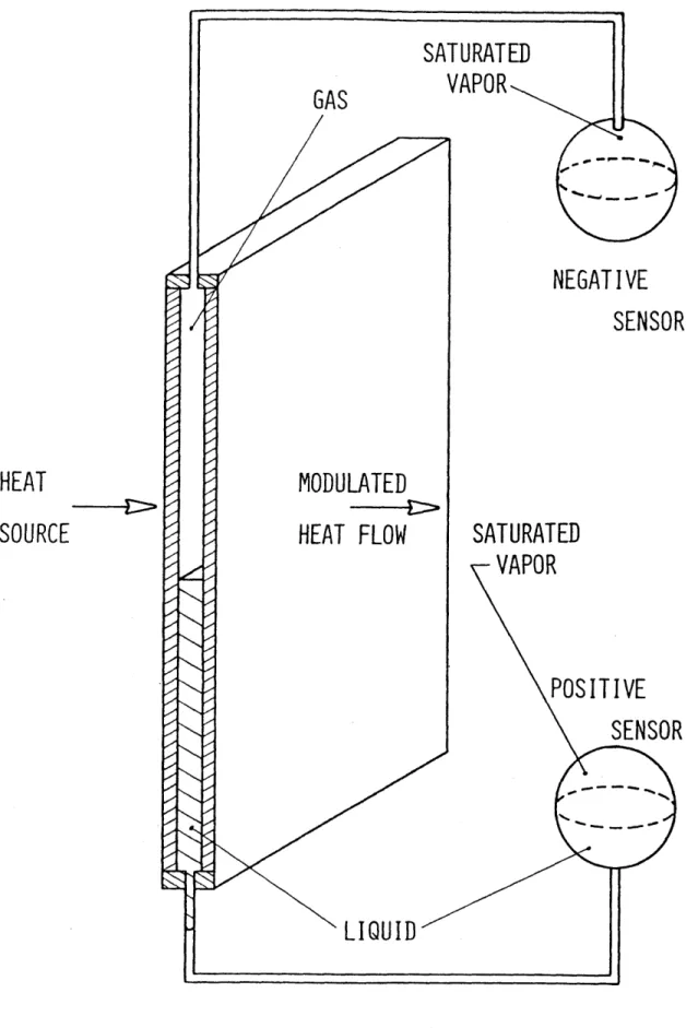
The amplifier has been defined as an effort amplifying de-vice, drawing power from a third port to perform its function. For a thermal amplifier the effort variable is temperature. Therefore a thermal amplifier senses a small temperature input, i.e., a small temperature difference above or below ground, and produces a large temperature difference at the output.
The amplifier designed and investigated in this thesis
employs two variable thermal resistors in a "push-pull" configuration. A schematic diagram of the internal amplifier circuit is shown in
figure 3-2.1. The resistors are placed in series, and the junction between them is the output.
The inputs change the thermal resistance of Rv and RL in-versely. A small positive (i.e. above ground or zero) temperature input on the positive terminal will cause Rv to decrease its thermal resistance and become more donductive. At the same time RL will in-crease its thermal resistance and become more of an insulator. The net effect is to create, for the junction, good thermal communication with the high temperature source, hereinafter just called the source,
and poor thermal communication with the low temperature source, called the sink. The temperature of the junction will rise closer to that of the source and away from that of the sink. Resistor R tends to "pull" the junction temperature up while resistor RL tends to "push", hence the term "push-pull". The reverse happens if a small positive
K:::J
HEAT
SOURCE
itonductance
It
nductance
C==>
HEAT
SINK
Figure 3-2.1: Diagram of amplifier thermal circuit.
-50-temperature is sensed on the inverting input. Resistor RL will become conductive, R insulating, and the temperature of the junction will
v
move closer to that of the sink. By symmetry, a negative (i.e. less than ground) temperature input at the noninverting terminal
will have the same effect as a positive input on the inverting terminal.
With no feedback loop the ratio of the temperature change at the junction to the temperature input is the open loop gain, A. With no input R & RL will assume equal values, and the junction will be at ground, that temperature mid-way between source & sink temp-eratures. With identical inputs on the inverting and noninverting terminals, the junction should again be at ground, since only differences are amplified.
This particular design was chosen for several reasons. First, the thermal resistance is the simplest thermal element that lends itself to thermal modulation. Control of the amplifier must remain completely in the thermal domain, temperature and heat flux must power all resistance changes. Second, temperature modulated thermal resistances can be conveniently constructed. The thermal conductively of various materials varies over approximately 6 orders of magnitude. Thus the same geometry can enjoy radically different conductivities by exchanging materials. And third, thermal resis-tance, or conductivity is a well tabled thermal property that is
-51-relatively insensitive to absolute temperature. For the amplifier properties to be predictable, internal component values must remain
constant over the temperature range of operation, or at least change in some predictable manner. Thermal conductivities for most materials are readily obtainable, and often the temperature dependence of this value has been tabled.
The above advantages combined to produce the amplifier with the circuit of figure 3-2.1. Note the similiarities of this circuit to the final stage of the P741 electronic operational amplifier,
shown in figure 3-2.2, (Ref. 8). This amplifier is the most commonly used electronic model. Instead of variable resistors the electronic amplifier uses transistors, labeled Q1 and Q2, but the method of op-eration is very similar. The output voltage depends on which trans-istor is most conductive. Transtrans-istors have the advantage of passing very little power when turned "off", behavior a thermal variable resistor cannot completely parallel. The difference, though, is not in structure, but in degree.
The theory behind the thermal amplifier could be made perfectly general by calling the temperature modulated resistors Effort Controlled Resistors (or ECR's). Effort, in this case temp-erature, controls their resistance value. Any power domain that has a resistor that can be modulated by an effort can also have an ampli-fier. This amplifier would work in the qualitative manner described.
-52-The next section is a more quantitative, linearized development, which makes some assumptions about the nature of the ECR.
EB
Figure 3-2.2: Circuit of p7 41 electronic operational amplifier final stage.
Section 3-3: Linearized amplifier description.
This section will present a linearized analysis of an ampli-fier with two variable thermal resistors. The term linearized means the resistors will be assumed to change their resistance linearly with input temperature. This is not a necessary condition for amplifier resistors. It represents a simplification of more complex or
non-linear resistance versus input temperature behavior. A non-linear approxi-mation is usually valid for a small range of operation. The behavior
of a non-linear resistor can be characterized as a curve on a resis-tance versus input temperature plot. If the curve is of low order
(i.e. has few deflection points) a small length of the curve can be approximated to first order by a line. The line represents a linear approximation of the actual behavior.
The goal of the linear amplifier model is to understand how fixed resistor parameters influence amplifier performance. There are many different types of thermal resistances, with vastly different characteristics. A rational choice of resistors requires understanding how their particular properties affect the amplifier. A quantitative expression for gain will be derived, in terms of fixed system para-meters, assuming simple linear resistance changes.
In figure 3-3.1 the amplifier circuit is shown with more detail. Electronic symbols have been used for the thermal elements because of their familiarity. For simplicity, ground temperature is chosen half-way between source and sink temperatures, this is a very
-54--[T
2- T- :
i=
ATIN
T
OTO-TG = AToUT
RV 2
-KATIN
V +2L
R, "
+ KAT,,
L 2 IN*V-
MAXIMUM RESISTANCE VALUE
L-
MINIMUM RESISTANCE VALUE
.
TouT+ ATs2
R
LATOUT:
R
LATS
R
V+R
L2
ATIN
GAIN
Figure 3-3.1: Amplifier gain derivation.
IT2
TG
ATs
RV +R
Lconfiguration in electronics. The source and sink are shown as batteries, with the source ATs/2 above ground in temperature, and
the sink ATs/2 below ground. All temperatures are referenced to ground, and appear as AT, meaning the distance from ground temp-erature. The total temperature drop from source to sink is AT .
s
The two effort controlled resistors, Rv and RL, are analogous to a voltage divider, but instead divide temperature. The amplifier output, T , is the temperature of junction 0, between
the two resistors. The output temperature can be determined if the resistance values of Rv and RL are known, as follows:
ATou AT R(3-3.1)
out
s
RL +
Rv
2
The value of R or RL will always be a positive, finite, non-zero number. From this expression it is clear the output can never be higher than the source temperature, nor lower than the sink. The ratio of the resistances divides the temperature between source and sink and produces the output.
If they are geometrically identical the variable thermal resistors, Rv and RL, will have identical maximum and minimum re-sistance values, designated rv and rL respectively. The value of rL, the minimum resistance of the variable resistors, can never be zero. There is a limit to how conductive any thermal conductor can be made, so rL will always have some finite, non-zero value. Conversely,
ý56-materials have finite thermal resistivity. There are no perfect in-sulators, and r , the maximum thermal resistance, will never reach infinity, but instead will have a finite value.
To quantify amplifier gain a specific expression for the linear thermal resistance changes must be assured. R and RL were characterized by the following inverse relations:
r + r v L R = - k ATin (3-3.2) where, ATin = [T1 - T2] r + r
RL=
v 2
+ k ATin
(3-3.3)
Both have a fixed resistance that changes with a constant increment
with input temperature.
The linearized constituitive relations of R and
RL
entail
that, with no inputs, each variable resistor will assume a value
mid-way between minimum and maximum resistance value. This is not
a necessary condition for a resistor used in an amplifier. By
assum-ing a zero-input, mid-point resistance value the derivation of a gain
expression is simplified. In the actual experimental amplifier the
resistors used did not conform to this assumption. The two resistors
do, however, have to assume equal values, for no input, if ground
is mid-way between source and sink temperature. Otherwise a zero
input would result in a non-zero output. The amplifier
out-put is above or below ground. This outout-put symmetry around the ground point is assured if the resistor range is symmetric about the zero-output resistance value. The zero zero-output resistance value is:
r -r
ro = rL + v2 L Rv = RL (3-3.4) and is the value assumed by R and RL for zero input. The (rv - rL/2)
term is half the resistance value between the minimum and maximum, which is then added to the minimum to get the mid-point value.
In the qualitative description of amplifier operation Rv
and RL were described as varying inversely for the same input. However, identical inputs of different sign should produce identical outputs of different sign. The amplifier of figure 3-3.1 will perform in this manner as if Rv and RL change their resistance the same amount for each unit of temperature input, above or below ground. The gain will remain constant over the full range of operation if each unit of temp-erature input produces the same unit resistance change over the full range of resistor operation. This is not a necessary but a sufficient
condition for a constant gain. Both resistors can be nonlinear and the gain remain constant over the full range of operation, if they
compensate for one another. An amplifier of this type will be dis-cussed in section 5. The assumption of unit resistance change simpli-fies a gain expression derivation.
Constant gain is most important for open loop amplifier per-formance. Closing the loop (i.e. feeding the output back to one of the
-58-puts) diminishes the impact of a gain change significantly. In figure 2-4.2 the amplifier output was expressed as a function of gain, for the closed loop multiplier circuit shown, and as a function of the multiplier factor.
The constant k is the resistance change per unit of temperature input. The sign difference between the two resistor constituitive expressions causes the opposing resistance changes in Rv and RL for a given input. Assuming the amplifier has no load the heat flow through the two resistors must equal the flow through one, since they are in series, or:
AT R A T out + AT /2
S(3-3.5)
Rv +
RL RL
The gain will multiply the input temperature and yield the output in terms of the input. Thus an expression for ATout is desired. Re-arranging yields:
ATout
out
RLAT
R + RL
As
(3-3.6)
2
Now substituting the previous expressions for R and RL:
ATout =
r
L
ATin =
AAT.
(3-3.7)
Gain
which is the desired relation. The gain is expressed in time invar-iant circuit parameters, which are also independent of the input or
output values. In the next section the individual parameters composing the gain expression will be examined in detail.
-60-Section 3-4: Gain parameters.
The gain of a two, effort-controlled variable-resistor
kAT
thermal amplifier was derived to be s with the assumptions of
r +r v L
the preceeding section. The ideal amplifier has an infinite or very large gain. The gain expression will be examined to understand how each term relates to the circuit of the amplifier, and how they might be used to maximize the gain.
The constant k is straightforward. A larger k means more resistance change for a given temperature input, and thus a greater junction '0' (fig. 3-3.1) temperature change, which is the output. Since the gain is the ratio of output to input, it is consistent to find k in the numerator; a larger k means a higher gain.
The total temperature difference between source and sink,
AT
s ,belongs in the numerator. The variable resistors act like a
temperature divider, the output is the ratio of resistances multiplied by the temperature difference, specifically,
AT
=AT
v
-1
(3-4.1)
A larger ATs results in a larger output and higher gain.
The most subtle terms in the gain expression are r and rL. The sum of the minimum and maximum resistor values appear in the de-nominator for non-obvious reasons. The total resistance of R and RL is always a constant, and equal to the sum of rv and rL, or:
Rtotal
=
Rv + RL
=
rv
+
rL
(3-4.2)If the total temperature difference, ATs , remains fixed, any increase
in rv or rL will diminish the heat flux through Rv and RL. The temp-erature difference across a thermal resistance is directly propor-tional to the heat flux through it. The highest gain amplifier will produce the most junction temperature change for a fixed resistor value change (k, the resistance change per unit of temperature input, has remained fixed). The amount of junction temperature change for a given
resistance change is directly proportional to the heat flux. Thus diminishing the heat flux decreases the junction temperature change
and diminishes the gain. Consequently both rv and rL appear in the denominator.
This, perhaps unforseen, result puts the amplifier designer
in a decision position. The denominator of the gain expression
con-tains both the minimum and maximum thermal resistance of the variable resistors. The amplifier power output will be greatest when rL has the smallest value, since rL is the smallest resistance possible
be-tween the output (or load) and the power source. Reducing rL also increases gain. Both these factors guarantee rL will be made as small as practically possible. Once rL has been established by tech-nological considerations, rv, the maximum resistance value, has to be chosen. The r value can usually be chosen since it is far easier
v
-62-to increase thermal resistance than decrease it. For maximum gain r should be made as small as possible. Decreasing r has the unfortunate
v
consequence of decreasing amplifier range. To understand qualitatively how r affects range consider the case where r is made almost as small as rL. This would be the maximum gain situation, but the output would hardly change regardless of input, since maximum and minimum resistance of the variable resistors are almost equal. In other words, they have become essentially fixed resistors, and the term range is meaningless. On the other hand, if rv is made very large, the amplified output can move over a range slightly less than ATs . But the gain is substantially
reduced because each degree of input temperature affects the ratio of Rv to RL much less, whichmeans less temperature change at the output. The choice of r is thus the pivotal decision.
V
A function relating gain and range to rv and rL is necessary. The maximum output occurs in response to an input that totally saturates the amplifier, and drives the two variable resistors to their minimum and maximum values. Analytically this means
rv - rL
k ATin(sat) 2 (3-4.3)
or k ATin assumes a value that makes Rv = rL and RL = rv. Putting
this value of kATin into the gain expression (eq. 3-3.7) gives:
r
r
AT v L AT (3-4.4)
out 2(rv + rL)
j
-63-The maximum output of the amplifier is less than or equal to 1
+ - AT . The output can never exceed the effort value of the source.
-2 s
The ratio of actual output to theoretically possible output can now be expressed. AT outr - r ffi(3-4.5) r +r 1AT v L 2 s
It is most convenient to have the ratio of actual to possible output expressed in terms of the ratio of r to rL . or:
r v
1
T r
out L
= Fraction Possible Range (3-4.6)
1 r
- T v
r
2 s rL +1
This function is plotted in figure 3-4.1 as the curve labelled range, as a function of the ratio r /r.L
The second curve shown in figure 3-4.1 is the gain function. This is the fraction of the theoretical maximum gain plotted as a function of r /r . The expression for gain is:
v L
Gain = k AT= (3-4.7)
r + r
v L
as shown previously. The maximum gain amplifier, in theory has rv = rL. The ratio of actual to maximum gain is expressed by the relation:
k AT
r+ r 2r
v L L (3-4.8)
Fraction possible gain k AT rv + rL
2rL L
-64-n
O
0) 0 ccw
0
z
4
U)
u
w Cu4 Io"
0 0 0 0 0o
•o
ot
o
39NVM
8O
NIV9
NO11WHVA
Figure 3-4.1: Fraction of gain and range as a function of resistance ratio.