The Design and Fabrication of Movable Micromachined Mirrors
ByMartin Scheidl
Submitted to the Department of Mechanical Engineering
in partialfulfillment of the requirements for the degree of
Bachelor of Science at the
PMassachusetts Institute of Technoloy
June 1988
© Massachusetts Institute of Technology 1988
Signature of author
Department of Mechanical Engineering May 6, 1988
Certified by , .. , , , ,
-Accepted
by-' / Rosemary L. Smith
Sinclaiifisiting Asst. Professor of Electrical Engineering Thesis Supervisor
/
Professor Peter Griffith man, Department CommitteeOF T~ThNGLOY
JUN 131988
N A LJI\ f I . UEM~ll~i
The Design and Fabrication of Movable Micromachined Mirrors
By
Martin Scheidl
Submitted to the Department of Mechanical Engineering on May 6, 1988
in partial fulfillment of the requirements for the degree of
Bachelor of Science in Mechanical Engineering
Abstract
Small movable mirrors made by using micromachining techniques have been designed and fabricated. After a brief description of semiconductor micromachining methods, the design of the miniature devices is described. There are both a preliminary and a secondary design described in the report. The actual devices are 2mm by 2mm silicon plates 10 gm thick attached to a silicon substrate by 8 tm thick polyimide beams. The plates have a metal coating which allows the plates to be electostatically deflected. A feature of the devices is an on-chip oscillator circuit which allows deflection measurement through capacitive sensing. Using adaptations of semiconductor processing technology, the devices are batch
fabricated, producing 17 mirrors with associated circuitry.on one 2-inch wafer. A section on fabrication and initial load deflection testing of some devices concludes the report.
Thesis Supervisor: Rosemary L. Smith
Title: Sinclair Visiting Assistant Professor of Electrical Engineering
Acknowledgements
Completing a research project like this one requires the help and encouragement of many. I would especially like to thank:
Professor Rosemary Smith, for providing the original idea of a different micromachined device and for providing enthusiastic guidance in this newly learned field.
Mark Allen, my partner in this project, who, with his experience and knowledge of the many aspects of micromachining and processing, made it possible to carry out this research. His humor has made even the longest lab session enjoyable.
Professor Nico de Rooij, of the Universit6 de Neucha^tel, Switzerland, for introducing me to this field of work and for providing the initial contact to the research group here at MIT. Marty Schmidt, for his interest and technical support.
My family, for their never-failing support and encouragement in my endeavors.
Table of Contents
Abstract ...
A cknow ledgem ents ... 3
1 .Introduction ... ... 6
2.Micromachining Techniques... ... .... .. ... ... 7
2.1.Materials Used ... 7...
2.2.Thin Film Deposition ... 12
2.2.1.Thermal Oxidation ... .... 12
2.2.2.Spin Coating...13
2.2.3.Evaporation ... 14
2.2.4.Chemical Vapor Deposition... 14
2.3. Photolithography ... .. ... 15
2.4.Etching ... ... ... . ... 16
2.4.1.Anisotropic Silicon Etching in KOH ... 16
2.4.2.Plasma Etching ... 17
3.Design of Movable Mirrors ... ...18
3.1.Design Goals and Initial Ideas...18
3.1.1.M irror ... 18
3.1.2.Support Structures... 19
3.1.3.Drive System ... ... ... 22
3.1.4.Sensing System ... ... ... ... ... 22
3.1.5.Findings from the Initial Design ... 22
3.2.Final Design ... 23
3.2.1.Mirror ... 23
3.2.2.Support Structures ... 25
3.2.3.Drive System ... 25
3.2.4.Sensing System ... 27
4.Fabrication of the Mirrors ... 29
5.Testing of the Mirrors ... .... ... ... ... ... 36
6.C onclusion ... 38
Appendix A: Beam Deflection Calculations...39
Appendix B: Process Steps for fabrication of movable mirrors ... 42
References... 46
List of Figures
1 The diamond crystal structure of silicon 8
2 Cubic crystal structure showing Miller indices 9 3 Model showing three low-level directions of silicon 9 4 Schematic diagram of a Czochralski crystal growing machine 10
5 Silicon dioxide growth rates 13
6 Schematic view of spinning apparatus 13
7 Schematic diagram of an LPCVD reactor 14
8 Patterning steps using positive photoresist 15
9 Anisotropic etching of silicon 17
10 Plot of wafer masks used to make original designs 20
11 Process steps for original design 21
12 Process steps to make suspended silicon plates 24
13 Beam designs for final design 25
14 Cross section of the final device design 27 15 Mask patterns used to make torsional mirror 28
16 Mirror fabrication process 30
17 Photographs of the three different beam configurations 31,32
18 SEM image of bending beam design 33
19 SEM image of the same bending beam device 34 20 Details of the plate-beam connection for the bending beam 35 21 Deflection versus applied voltage for torsional beams 37 22 Log -log plot of deflection versus applied voltage for torsional beams 37
1.Introduction
Micromachining is a technology which has been growing as a result of the increasing demand for small, inexpensive parts and sensors for applications ranging from active suspensions in automobiles to more sophisticated medical probes for the accurate diagnosing of illnesses. As micromachining slowly moves from producing interesting gizmos to becoming recognized as a valid engineering method, an emphasis is being placed on fabricating useful items on a large scale. The increasing miniaturization and complexity of mechanical and electrical hardware will tend to favor the increase of micro-machined products.
This project of designing and fabricating movable micromachined mirrors started innocently as a simple interest in the possibilities of a new type of processing. Now , after many months, an idea has been developed, and a product has been made. Using traditional and some non-traditional techniques of semiconductor processing, a 2 mm square
deflectable mirror has been fabricated. Initial tests indicate that the mirrors can be controllably moved with electrostatic forces. Further work is needed to refine various processing steps for the optimum performance.
This work is organized as follows. After a brief description of the micromachining processes used in the fabrication of the mirrors, there is a description of the design of the devices.This section is followed by a section on fabrication and the results of preliminary voltage deflection tests.
2.Micromachining Techniques
Since the features of micromachined devices are on the order of microns , standard machining techniques can no longer be used effectively. There is little, if any, tool-workpiece contact. Instead, the "shaping" or "patterning" of the tool-workpiece is performed through intermediate agents such as chemical solutions that selectively etch a material. This technology is directly adapted from the methods used to manufacture electronic integrated circuits. In the making of these circuits, various materials are deposited onto a
semiconductor substrate as thin films or as oxidations and then patterned using lithography and etching techniques.
The basic techniques used in both electronics manufacturing and micromachining are thin film deposition, photolithography, and etching. In processing, thin films are deposited on a substrate (usually a silicon wafer), patterned, and etched into that pattern. This
patterned film can then be used as it is or as a subsequent pattern for an etching step. For electronic applications, structures are more or less planar, being built up to maximum heights or depths of 20 gm [1, 2]. To build the three dimensional structures desired for mechanical devices, one must be able to make features that are much deeper; they often must be as thick as the substrate itself. Accurately controlling the way material is added and removed is a problem that must be addressed for each micromachining application. It is the
emphasis on advancing processing steps for high precision, three dimensional shaping operations that set micromachining apart from standard electronic semiconductor processing.
The subsequent sections will give a more detailed explanation of the materials and micromachining techniques used to prodnce the movable mirrors.
2.1.Materials Used
Silicon is the most commonly used material in micromachining.The combination of its anisotropic etching properties and its well researched mechanical and electrical properties make it the material mcst suited to hybrid electrical and mechanical devices. The other materials that are used have been mostly adopted from integrated circuit applications. These include thin films such as polysilicon, various nitrides, polyimides, oxides, and metals
[3].
The materials used to make the movable mirrors are single crystal and polycrystalline silicon, silicon dioxide, polyimide, and aluminum. The mechanical structures are of single
crystal silicon and polyimide, and the circuitry is of the silicon substrate, silicon dioxide, polysilicon, and aluminum.
Silicon
Bulk silicon is the primary material used in micromachining. A very common element on the earth, silicon by itself is not useful for micromachining or circuit fabrication unless it is extremely pure. Modem purification techniques allow people to make silicon that is 99.9999999% pure [1,3-5]. Pure silicon can exist in both a single crystal and a polycrystalline state, depending on how the material is processed.
The most common form of silicon used in micromachining is single crystal silicon. It is used because it is readily available, is very uniform, can be etched anisotropically, and it
has good, predictable mechanical properties. Since silicon has been the material almost exclusively used to fabricate integrated circuits for the past twenty five years, an enormous
amount of information is available on the subject. Silicon's behavior under many different circumstances is well known [6,7] Only a brief overview of these characteristics will be given here with respect to the applicability to the design and fabrication of micromachined mirrors.
Silicon forms a diamond crystal structure, which can be described as two interpenetrating face-centered-cubic sublattices, with one atom of the second sublattice located at one fourth of the distance along a major diagonal of the first sublattice (fig. 1). Miller indices are commonly used to describe silicon crystals. This type of notation can indicate planes, directions, or a related group of planes or directions. In figure 2, notation such as (100) designates the plane which is perpendicular to the [100] direction. As another example, the notation <100> designates the set of directions [100], [010], [001], [100], [010], [001].The notation ( 100) is used to describe the set of planes perpendicular to these
Fig. 1. The diamond crystal structure of silicon [7]
M. Scheidl, Thesis page 8 U1.1-M LI011S.
7
(100) plane
(111) plane
)10] direction
X
Figure 2. Cubic crystal structure showing Miller indices
The atomic packing density of silicon is different when a crystal is viewed from different directions. Figure 3 shows pictures of models of silicon crystals taken from different low-index directions. The photogragh in the <100> direction was taken at an
angle 54.750 from the one in the <111> direction, and the photograph in the <110> direction is 900 from the <100> direction. One can see that the <110> plane has the lowest packing density and the <111> plane has the highest. As a result of the differences in packing density, each direction has a different elasticity constant and a different ultimate tensile strength [8]. The <111> directions exhibit the highest elasticity and the highest ultimate tensile strength. As a result, silicon tends to cleave along these planes [9].
<111> 3 M s0> <110>
Figure 3. Model showing thr'ee low-level directions of silicon [10]
For the mirrors, silicon is used for both its mechanical properties and for its electrical properties. From a mechanical standpoint, silicon is a tough material. It has a yield strength of 7.0 x 10⁹ Pa. The yield strength of maximum strength steel is only 4.2 x 10⁹ Pa. The modulus of elasticity does vary depending on the way a crystal is oriented, but the accepted general Young's Modulus for silicon is 1.91 x 10¹¹ Pa [11,121. Poisson's ratio is also dependent on direction, but a general value which can be applied is 0.4.[6] The electrical characteristics of silicon have been much more exhaustingly researched, but it is not necessary to go into them here. It suffices to say that for the application to the circuits for the mirrors a p-channel MOSFET process was employed which produces properly
functioning transistors, resistors, and capacitors on the same n-type silicon substrate as the mirrors[5].
The silicon which is used in integrated circuit manufacturing and micromachining is in the form of wafers 2.to 6 inches in diameter. These wafers are produced in the following process: after metallurgical grade silicon has been produced in a submerged-electrode arc furnace, it is made into boules produced by the Czochralski growing technique. In this technique, a seed crystal of known orientation is touched to the surface of molten silicon. It is then pulled up, puliing the newly forming boule of silicon with it. As the molten silicon cools, it hardens into one crystal oriented to the same direction as the seed crystal. Figure 4 shows the Czochralski growing apparatus in a schematic view. A typical boule of silicon formed by the Czochralski method weighs about 60 kg and is 100 mm in diameter and 3
meters in lenogth rl3 141 Cruoible (graphile or quartz r or ilor Water cooled enclosure -Thermocouple rf power (or integral resistive heater) ntlroller
outletf a Czochralski growing machine
Figure 4 Schematic diagram of a Czochralski growing machine [13] M. Scheidl, Thesis page 10
To make wafers, a boule is first turned on a lathe-type machine which creates a silicon cylinder. Slices are then cut off to produce wafers. The directions of the silicon planes are determined using x-ray crystallography and then a "flat" is cut into the edge parallel to a desired crystal plane. The wafer is polished and then is ready for processing.
Polycrystalline silicon has quite different properties and is made differently than single crystal silicon. For the mirrors, it is used in the circuits and not in the mechanical
structures. In the circuits the polysilicon is heavily doped and acts as a conductor for the transistors built on the silicon substrate.
Silicon Dioxide
Silicon dioxide is another material which is often used in micromachining. It is often an etch mask for silicon, but it has also been used as a structural material on its own to make cantilever beams [15].
The circuit uses silicon dioxide as a passivation layer between conducting layers of metal and silicon. This material also serves as an etch mask for the etching of the large mechanical structures.
Polyimide
The beams which support the silicon mirrors are made of polyimide. An example of polyimide use is as the base of the flexible circuits commonly seen connecting movable print heads to the controlling electronics in computer printers. The particular type used for this project is a benzophenone tetracarboxylic dianhydride-oxydianiline/ metaphenylene diamine polyimide (BTDA-ODA/MPDA). This material was chosen for its low modulus of elasticity and its adaptability to the fabrication of the movable mirrors. For the polyimide used, Young's modulus is 3 x 10⁹ Pa. There is also a residual tensile stress of 30 x 106 Pa in the material when it is built up as a thin film [16]. In the fabrication process, the
polyimide is applied as a viscous liquid which is the polyamic acid precursor of the polyimide dissolved in N-methyl pyrrolidone and spun on the wafer. It is later cured at 4000C to form the polyimide.
Aluminum
To make electrical contact between the different parts of a circuit, a metal such as aluminum is deposited on a wafer. The deposition *akes place in a filament evaporator, where, under high vacuum, aluminum is evaporated off of a heated filament and deposited on a wafer.
For the mirror devices, aluminum is deposited in two steps: one to provide electrical contact within the circuit and one to make the drive and sense plates of the mirror and connect them to the circuit.
2.2.Thin Film Deposition
With the exception of the single crystal silicon substrate, the materials used in the fabrication of the mirrors are all deposited or grown as thin films. Only those techniques which apply to the fabrication of the mirrors are discussed here.
2.2.1.Thermal Oxidation
Silicon dioxide is grown on a silicon substrate through thermal oxidation. The process relies on an oxidation reaction which takes place at the interface between silicon and silicon dioxide. The chemical reactions are the following:
Si(solid) + 02 -> SiO2(solid) (1) Si(solid) + H20 -> SiO2(solid) + 2H2 (2)
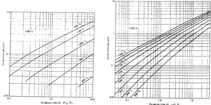
Oxide forms on silicon anytime there is oxygen present. At normal room conditions a maximum 20A layer of oxide forms rapidly (equation 1). To grow more oxide one must expose silicon wafers to oxygen at higher temperatures.This technique allows more oxygen to diffuse through the building oxide layer to react with silicon at the Si-SiO2 interface. One
can also use oxygen saturated with water (wet oxygen) to increase the diffusion of oxygen even more and thus increase the oxide growth rate (equation 2) [3,17,18]. One can see the difference in growth rates for the different types of thermal oxidation in figure 5.
A7-'I II \''
.1fdf
0 0 10 100 Oxidationtfrm (h) JIy C0IiJ
10I
4
9-Ow'dallon ifme th) Wet Ot
Figure 5. Silicon dioxide growth rates [181
2.2.2.Spin Coating
Spin coating is one method used to spread a thin layer of a material on a wafer. Figure 6 shows a schematic diagram of the apparatus used. The material to be coated on the wafer is originally in a liquid fornm.t is poured or dripped onto the wafer and then the wafer is spun for 30 seconds, planarizing and spreading the material to a desired uniform
thickness.The viscosity of the liquid and the spinning speed control the thickness of the applied coating.
In the fabrication of the mirrors, photoresist and polyimide are deposited on the wafers with the spin coating technique.
1"rv,.. " -at- l.,
n-Wafer
\huck holds wafer with
Figure 6. Schematic view of spinning apparatus
M. Scheidl, Thesis page 13
0 001 U0 fV ; i I i i I , ;:i I
1
I
---& L-J"I 17
-L
Iicnes
rnps
2.2.3.Evaporation
The aluminum which makes contact to the electrical parts of the devices is deposited on the wafers in a filament evaporator. This device is a vessel under high vacuum where aluminum is evaporated off of a hot filament. Everything in the vessel becomes coated with a thin layer of aluminum, including any wafers.
2.2.4.Chemical Vapor Deposition
Chemical vapor deposition can be defined as a natural synthesis method in which the constituents of the vapor phase react to form a solid film at some surface [19].
Polycrystalline silicon, or polysilicon, is made by pyrolizing silane (SiH4) at 600 to 6500
C. The chemical reaction is
SiH4 - > Si + 2H2 (3)
Polysilicon for the mirror circuits is made in a low pressure chemical vapor deposition (LPCVD) reactor. In this reactor, the wafers are stacked inside a furnace tube at pressures of 25 to 130 Pa (0.2 to 1.0 torr) while silane is pumped across them. As the reactant vapor contacts the wafers, a film of silicon forms on them while hydrogen escapes and is pumped out of the reactor. Factors such as the temperature, the compositions of the gases pumped through the reactor, the flow rate, and the pressure affect the deposition rate and the structure of the polysilicon [19,20].Figure 7 shows a schematic representation of such a reactor.
End cap
Exhaust to pump
Figure 7. Schematic diagram of an LPCVD reactor [19]
2.3.Photolithography
Micromachining and integrated circuit processing take advantage of the precise patterns that can be duplicated using photolithography. The technique is a method of transferring patterns which have been made on a mask to many wafers. Figure 8 shows this process schematically. As in the diagram, positive photoresist was used for all patterning steps in the mirror processing. This type of resist is more forgiving with exposure and development times and less toxic than negative photoresist. The type of resist used also determines how the masks are to be made -either the positive or the negative image of the desired pattern. For the processing of the mirrors, positive image masks had to be made.
-Masking film Silicon
5 5 Photoresist
Glass mask
Figure 8. Patter
1.Masking film on silicon
2.Positive photoresist spun on over masking film
3.Contact mask placed on wafer, pattern aligned, and resist exposed to UV light
4.Resist developed (section exposed to UV light dissolves)
5.Masking film etched to pattern
6.Photoresist stripped or etched away, leaving masking film in desired pattern on silicon fning steps using positive photoresist
The minimum pattern dimensions for the mirror devices are 5j1m. At this level of detail, the quality of the masks, the exposue time, and the development time become important factors in producing a true replication of the mask pattern on the wafer.
2.4.Etching
Once a pattern for a material has been placed on the wafer by photolithography, it must be transferred to that material. Etching accomplishes this transfer by using the pattern as an etch mask. Often the material patterned by the photoresist is itself a pattern for a further etch. Such is the case with the etching of silicon in potassium hydroxide. Photoresist cannot be used as an etch mask for KOH; thus silicon dioxide patterned by photoresist is the etch mask. Following these steps, one sees that the transfer of a pattern to the final material that is to have that patten might involve more than one intermediate patterning mask step.
The etching processes used to make the mirrors were mainly KOH etching of silicon, 02 and SF6 plasma etching, and wet oxide and aluminum etching.
2.4.1.Anisotropic Silicon Etching in KOH
The etching of silicon is one of the important components of micromachining. Potassium hydroxide as an etchant has been very successful and is frequently used [10]. KOH etches silicon anisotropically, with etching in the <111> directions occuring much more slowly than in other directions. Recalling the structure of silicon shown in section 2.1, a wafer in the (100) plane will have four (111) planes intersecting it at an angle of 54.70, which are themselves at right angles to each other. This geometry is frequently used to etch rectangles and squares. It is also used to etch pyramidal pits. Figure 9 shows some results of anisotropic etching of silicon.
.70
Etching along (111 }planes
Pyramid shaped pits to form membranes
Figure 9. Anisotropic etching of silicon
Although it is not exactly known how silicon etches selectively along different crystallographic planes, it is believed that the spacing between the planes in a particular direction limits the etch rate [12,21]. In silicon the <111> planes have the closest spacing while the <100> planes have the greatest spacing. The anisotropic etching characteristics thus seem to indicate that the etch rate theory has validity.
To etch the wafers on which the mirrors were built. a 20% KOH solution in water at 560C was used. The etch rate was approximately 20tm per hour.
2.4.2.Plasma Etching
Plasma etching is often referred to as dry etching, since the etching medium is an ionized gas which reacts with the material to be removed. The etching process takes place in a vacuum vessel which has two parallel plates on the top and bottom. The plasma is excited by rf discharge. Wafers are placed on the lower plate and exposed on the topside to a flow of plasma. Although the mechanism of plasma etching is not fully understood, the causes of etching are thought to be chemical reactions with the active species and ion
bombardment[22].
Plasma etching was used in the fabrication of the mirrors to etch photoresist and to clear the beams from the silicon substrate in the final step.Oxygen plasma was used to remove photoresist and SF6plasma was used to etch the silicon.
M. Scheidi, Thesis page 17 I
3.Design of Movable Mirrors
Optical scanners have been previously fabricated out of silicon plates held by thin silicon beams and optical displays have been made out of silicon dioxide beams[12,15]. The scanners are driven at resonant frequency by outside vibrations and the optical display operates mainly as a multi-element light switching device. The idea which prompted this project was the belief that a statically controllable mirror could be designed that would accomplish in one device what both of the other devices could do.
The process from initial goals to the present design for the mirrors are described in the next sections.
3.1.Design Goals and Initial Ideas
The desire to fabricate a suspended plate which could act as a mirror from a silicon wafer initiated the first designs for a statically positionable micro-mirror. The design goals were set to allow for a practical and usable design. These goals were:
1. The mirror must be mechanically stable; it cannot buckle or bend unacceptably due to either outside loading or intrinsic stress.
2. The mirror must be able to rotate about 4 degrees from the horizontal. 3. The mirror must be at least 2 millimeters square on a side.
To develop a sense of the requirements set by these criteria, some initial mechanical structures were designed. The initial thoughts were to make a simple device that could be fabricated entirely out of silicon. Such a device could be made using silicon
micromachining techniques that are often used and well researched. With the initial structures fabricated, research could be done to determine optimal sizing of the mirror plates and supporting beams for a secondary design.
3.1.1.Mirror
The mirror had to be a minimum of 2 mm square; thus the size of the plate was determined. Machined out of silicon, it would be minimally 10gm thick to make it stiff and tough enough to last through the long processing sequence. A thin layer of metal would be
evaporated on the top surface to provide a reflective surface. This metal surface could also act as an attracting plate to be used to electrostatically deflect the mirror.
3.1.2.Support Structures
From the beginning, the support structures for the silicon plates were seen as the most critical part of the mechanical design. The sizes and orientations of the support beams would determine whether the mirrors could deflect in a uniform and controllable way. Since the emphasis of the initial design was to try many structures in order to have a sense of the more effective configurations, not many preliminary analyses were done on the possible beam structures. For simplicity in processing, the beams were designed to be of silicon. Ten different configurations were initially designed. These structures can be seen in figure 10.
Figure 10 is the combination of three mask levels superimposed on each other. The first two masks help form "island structures" the size of the mirror plates using anisotropic etching from the backside of the wafer. The last mask is used to form the support structures from the front side in a plasma etch step. This process for two of the beam designs is shown in figure 11.
L --- Lj--0
ZigureZ
ILI02
Itl
}
el
Figure 10. Plot of wafer masks used to make original designs
Side view
a.silicon substrate View of backside
b.patterning of plate; thickness determined in this step c.continue etching to make island d.patterning of beams from topside beams beams View of topside
Figure 11. Process steps for original design
3.1.3.Drive System
Since the object of the design was to produce a statically controllable plate, a drive for the mirror had to be stable, and above all quickly controllable. Several schemes were considered, including bimetallic strips which would deflect under different voltages applied across them. The best drive system was decided to be an electrostatic drive,
beacuse it could provide fast and possibly powerful response When connected to a sensing system through a control circuit , the electrostatic drive could provide the necessary forces to hold the mirror in a fixed position.
3.1.4.Sensing System
Assuming that the support beams were to be made of silicon, it was not difficult to decide to use the piezoresistive property of doped silicon to make diffused resistors for sensing stress changes in the beams. The resistors could be wired in a wheatstone bridge configuration to give signals relating beam deflection to output voltage. The resistors would
be placed at the ends of the beams where there is the most stress, similar to the way diffused resistors are placed on silicon diaphragms used as pressure sensors[12].
3.1.5.Findings from the Initial Design
The processing of the initial wafers did not progress very smoothly, and only
qualiltative results were obtained. One wafer successfully went through the entire process, but only a few of the devices survived.The most important result was that the silicon beams were far too stiff to allow noticable deflections with reasonable voltages.The
voltages that would be needed to deflect these mirrors were calculated to be 350 volts.for a deflection of 40
3.2.Final Design
Not long after the original design was found to have beams that were much too stiff, an improved design began to take shape. Since silicon was much too tough for the support structures, it was decided to use a material with a much lower modulus of elasticity. The material that would be used for the new beams would be polyimide. This material is used in semiconductor processing as a planarizing medium and as a packaging material to keep contaminants from finished electronic devices. It has been found to be uniform enough in its mechanical properties that it has been characterized[ 16][see also section 2.1].The fact that silicon beams could no longer be used also caused a re-evaluation of the sense system, since diffused silicon resistors are not possible for polyimide beams. Instead, a capacitive sense system was devised, in which a plate on the mirror would act as one side of a variable capacitor. This capacitor would be part of an oscillator circuit which changes its oscillation frequency with a change in the sense capacitor on the mirror. These major changes in the design required many refinements in the design of the masks and the process. Nevertheless, the original goals were kept the same.
3.2.1.Mirror
The mirrors in the new design remain the same as in the old one -thinned silicon plates.They are produced by first etching a 40 gm thick diaphragm from the back and then patterning the plates from the front, where they will be etched to their final thickness (6 to 9 gLm). They remain as plates on the diaphragm up to the last step, when the diaphragms are etched from the back with SF6 plasma until the plates clear. At that point in the
processing sequence, the beams are already patterned and can support the plates.Figure 12 gives a schematic diagram of this process flow.
a. original silicon substrate
b. diaphragms etched from backside
c. patterning of plates from topside -etch both sides
d. deposition of polyimide
e. patterning of polyimide (example: bending beam design)
f. cleared plated after backside plasma etch
Figure 12. Process steps to make suspended silicon plates
M. Scheidl, Thesis page 24
7
3.2.2.Support Structures
For the new design, the support structure was completely redone. Polyimide now supports the silicon mirrors, and the dimensions of the beams reflect the results of analysis of the possible beam structures. This analysis showed that the beam sizes needed to hold a 10 gm silicon plate flat are smaller than was expected. Cadculations were done for the three different designs; the bending beam design and the two torsional designs.
Bending type Torsional end Torsional middle Figure 13. Beam designs for final design
The dimensions of the beams were calculated using standard beam formulas adapted to plates, since the beams holding the mirrors are very much wider than they are
thick.Calculations were done that would relate angle of deflection to force and force to voltage applied between the conducting plate and the mirror. For the bending case, the relation is:
32Eab30d2
V2 = (1)
3eoAl(l + 2D)(1- v2)
where E is Young's modulus, 0 is the deflection angle, E- is the permittivity of air, d is the spacing from the mirror to the attracting plate, A is the area of the drive plate, v is
Poisson's ratio, and the dimensions of the beam are: width=2a, thickness=2b, length=l.
M. Scheidl, Thesis page 25
I I I , I II ,111I Ir II1 11 )) 111(111 11 1 I I 111I(II I) I (II( III I I I I I )III 111( I I I I L I II I I( I I I I I ) ) I )I 11I ) ) I I I I ( I) I I (I I 1I I ( I II II 1 I I ( II 1 I ( I ( I ) I I ( 1 I () I I I I ) I I( I ( ( III) I I ( II ( I I ) I I I I I IIII ( )1((11111)111111111 I) I I II I It I 1111111111111111 (11)1((1))( 1 I ) 11))1 1111)1 IIIIIIIIIIIIl) ()I I (II II II 1 (( IIIIIII))( I I t I I II:II I ( 111 I ( 11 I ) I ) (I I:( 1 11))1 I ) I I ) III IIII ) I ( I 1 1 1)11 I 1(1(1111( I ( It 111 I 11111I)( 1 I ) I II) I ( I ()I ( ) ) I I II II I I I I I ( ( II I 1 t I ) I I ) I I I ) (I I ( II I ( I I I I) I III I I ( L I ( I(( I I I I I ( I I) IIII I ) I 1 ( 1111111(1 I I ) 11111111 I 1 ( 11111 (1)111) II II 1 I)I ()(1( II 111111 I I I)I ) II ( II ((1(()1))1)11 I 1) )1111) IIlt I I ) i 1 · I · · 1) · L I·1 I I 11 ) IIIIIII I 1 I I I I I (·I I I I ( I I I ) I I 1~1 111111111111 111 (111((111 1 ( I 11 ( 11111111I11)))11· I 1 L (II)1I11111)1 I· I· I )1) I I I ) II I I t I I ) I( I I ) III I I rI II I I ) ·) I ) ( I I( r I ( ( ) I ) I I ( I 1,II 1 r I I r , r I I I I I I t I I I I I , I I I I 1 1111(1 1111 1 111 1 111111 I 1 1111(1)11 1.1 I IIII ( I · t L I I II I ( 1 I 1(1)111(11((I 1 1111111 i)~~ ) · I I I ) ( I
For the torsional cases, the formula is similar:
8EOd2ab3[16/3 - 3.36(b/a)(1 -b4/12a4)]
(2) 3E01AD(1+ v)
The constant D is the distance from the beam to where the center of electrostatic force is acting. Thus, for the torsional end design and the bending beam design, D = 1.5mm and for the torsional middle design , D = 0.5mm. The derivation of the formulas is given in Appendix A.
Using equations 1 and 2, a spreadsheet program was used to calculate the different voltages needed to move the mirrors through angles between 1 and 4 degrees.From the many calculated results, the final values for good beam sizes were chosen as a compromise between the requirements of each design and the ability of the process to produce them. Tables 1 and 2 show the final beam sizes and the calculated voltages needed to deflect mirrors held with these beams.
Table 1 Beam sizes for final design
Bending tvoe Torsional end Torsional middle
Beam Thickness 7gm 7gm 7gtm
Beam Width 200gm 150gtm 100gm
Beam Length 500gm 500gm 500gm
Table 2 Voltages needed to deflect mirrors of different designs
Design
Bending beam Torsional end Torsional middle
Voltage needed (Volts)
for 20 deflection for 40deflection
29.3 41.3
33.4 47.2
38.3 54.1
M. Scheidl, Thesis page 26
~-3.2.3.Drive System
The drive system for the final design still remained an electrostatic one, but the configuration of the attracting plates changed. The reason is that the sense system changed to a capacitive sensor, and half of the mirror plate had to be alloted for the sensing
plate.The mirror is driven from below with a charged plate underneath the device.
3.2.4.Sensing System
As stated, the position sense system could no longer be of piezoresistive silicon and thus another scheme had to be devised. A capacitive sense system was designed, with a capacitor plate which should vary its position being placed over half of the mirror surface. Another capacitor plate surrounds the mirror. A glass slide over the device has a metal coating and acts as a conducting plate between the capacitor plate surrounding the mirror and the plate on the mirror. This varying capacitor setup is part of an on-chip circuit which is a ring oscillator. The changes in the capacitance of the sense capacitor cause the oscillator to vary in its frequency output. This change can then be measured and decoded into
displacement readings with an off-chip processor.
Figure 14 shows a cross sectional view of an entire finished device as designed and figure 15 shows a plot of one device as it was drawn on the mask-making CAD terminal.
te and drive plate)
strate
Figure 14. Cross section of final device design
~1 OriqjC PoSe P~cl
j
.1 A L. .-r fr: J CircudiFigure 15. Mask patterns used to make torsional mirror
M. Scheidl, Thesis I
I-j
i page 28Re ft rem c,
TorSiomal
ffe -mi.'
4.Fabrication of the Mirrors
The fabrication process for both sets of mirrors was long and filled with setbacks, but working devices were ultimately finished .Figure 16 gives an overview of the fabrication process and appendix B gives a detailed account of the steps which were followed to make the final design of the mirrors. The process includes the manufacture of the oscillator circuit using a p-channel MOSFET process used in the MIT student lab. At the time of writing, a set of mechanical only devices has been produced. The combination wafers with both the mechanical devices and the circuits still have to be run through the final steps of the PMOS process before releasing the mirrors.
The next pages show photographs of the different devices taken during processing.
Backside etch bTopside eth
Topside etch
cPMOS
.rcess
PMOS Process Polyimide depositione.
Second metal deposition
Figure 16 Mirror fabrication
mechanical and n process, showing integration ofelectrical components
M. Scheidl, Thesis page 30
LiA
i 1c ufasion al middle{ designi o e i w hun Jo 4o h ye UoonI VhCU ens Ceion
Figure 17 (b). Torsional end design
M. Scheidl, Thesis page 31
-rn-rn-Figure 17 (c). Bending beam design
>lyimide beam
* .·," '." · .7?\.'
*a '..rP'lte
Figure 18. SEM image of bending beam design - in this picture one can see that the silicon plate is flat
Polyiinidt ICbams
--
N
.
'N-,
Figure 19. SEM image of the same bending beam device
M. Scheidl, Thesis page 34
/ / /
7
-9. 9.-. 9.Figure 20. Details of the plate - beam connection for the bending beam the
polyimide makes a very sharp step and can still can k,%eep the plate stable
5.Testing of the Mirrors
A few mechanical devices were finished, and simple deflection tests were done. Unfortunately , many of the polyimide supporting beams ripped and only the torsional end type devices were usable in tests. Although the other types of devices had beams of the same thickness, the torsional end type was more robust.
For the tests, devices were broken into individual pieces and coated with a thin layer of aluminum in the filament evaporator. The test apparatus consisted of a probe station which had a height measuring device attached to the microscope head. As the mirror plates were electrostatically deflected, the microscope focus was changed to keep the plate's edge in
view. Changing the focus moved the microscope head and thus enabled one to obtain deflection readings. Figures 21 and 22 show the graphs of the voltage -deflection data. The results are consistent from one test to another and from one device to another. The logarithmic graph gives an indication of the exponential relationship between voltage and deflection. The slopes of the experimental data plots approximately match that of the calculated results, although there is an offset. This offset is probably due to the need for a certain initial activation voltage to produce a deflection of the actual plates.
The actual results agree somewhat with the theoretical predictions. There are several possible reasons for discrepancies. One is the fact that these wafers have been the first ones
through the new process, and the necessary control on the processing parameters has not been achieved yet. The polyimide beams are quite small, and any over etching will
significantly reduce their dimensions and change beam characteristics. In addition, they do not have a regular cross section along the length of the beam. The control of the etching of the beams (step 69 of process in appendix B) needs to be controlled better. Additional stresses in the beams have also been introduced by the aluminum coating the topside of the devices. Another explaination for discrepancies could be the non-linear behaviour of the plate in the attraction field.
Deflection vs. Applied voltage
for a torsional beam
o o,0* 0 0 U - E dr 0. o 0 (p U
VC r
0 0 s ONn nan * Beam I Runl O BeamlRun2 0 Beamn2 0 Theory 0 I n 0 5 10 15 20 25 30 35 40 Applied voltage (V) 45Figure 21 Deflection versus applied voltage for torsional beams
Deflection vs. Applied voltage
for a torsional beam 100 Deflec- 10 tion(gLm) 1 1 10 Applied voltage (V) * Beam 1 Runl 0 BeamlRun2 M Beam 2 O Theory 100
Figure 22. Log-log plot of deflection versus voltage for torsional beams
M. Scheidl, Thesis page 37 b Deflec-tion(gm) 40 30 20 10 n m v ;i- - m i a C n r I-E v I I W I I B U V
6.Conclusion
Movable micromachined mirrors have been designed and some were successfully fabricated and tested. The original design goals have been adhered to, even though the sensing portion of the devices was not completed. There still remains to be much work done in perfecting the processing of the devices. The difficulty with suspending a silicon plate from polyimide arms lies in the controllability of the polyimide patterning and etching. It is this difficulty with predicting what actually happens to the polyimide during the etching in positive photoresist developer that most likely caused the force deflection tests to
produce results different from predicted ones. In all the tests, the polyimide was weaker than calculated. The photographs show that the actual shape of the polyimide arms varies and is not uniform from one device to another (see fig. 17).
Even though the entire process was not completely finished, the planning and design showed good results in the mechanical devices. The many processing steps produced the desired devices, and initial tests showed predictable voltage-deflection characteristics.
The success in making these mirror devices leads one to speculate on possible uses for these devices. Possibilities exist from miniature optical tables for aiming lasers to image scanning machines that could either record or send pictures. With a slight modification of the membranes and the beams, small microphones or speakers could even be made.
Appendix A: Beam Deflection Calculations
For the prediction of the bending and torsion of miniature polyimide beams, standard formulas are used from references 1261 to 1311. In each case, a point load is assumed to be acting on the bending plate. There are lower bound and upper bound calculations which are related to the positioning of the point load.
kb P Bending Case
-Za,
Sji a'5le crL doflrot;o h
crosS - gctr a
of bc v..
At the end of the beam there is both a downward force ad a moment applied. Using standard beam formulas applied to a plate, one substitutes for Young's modulus E:
poi-ssois rctk'o o4tc~ io , clue +o ;0rc.C p a>,~e.~~ ~(~t a ue, 4, ~~~I*~)P~ M 9,~, · 6, cI (f a'b- IrAbIL O 5 aiec44~2
Substituting for E and I :
Solving for P:
F
El -
? R
?Fk
oinIZ)(IV
c0
+gE-b?
The lower bound is approximated when D = 2mm, and the upper bound is approximated when D = lmm
M. Scheidl, Thesis page 39
\I
Torsion ca
Ire--l---Le -I
3(0+V)
t k~C .. ~.r.,,,..J,J ~1,jj1jJJLAiJwzzz
-ro roev6-c.[17
=t~,n tp? view3ýPD(Ifv)
3 jl ~ Qq 4 ji 6 roSS -ssctioSolve for P: zESay -2.3ci
Again, D varies depending an upper or lower on whether bound is being calculated+V) Again, D varies depending on whether an upper or lower bound is being calculated Electrostatic attraction is described by this formula:
6 A V
zfo~ce --n~Z
~~.~e(r*. 60~ -~ .+ dch tc A - Of1rdietTA d ta v- Sc(a 3f ~CkrGC(a7)
Solving for V2:The force to pull down the plate is twice P, since there are two beams. Thus
v
M. Scheidl, Thesis page 40
ch6
A *VW4
ase
-6,1k V,.Ojvlvs.
To obtain the voltage needed for a certain deflection, substitute for P. Bending: Torsion: VZ.
L56
-3.36-
I -03E,, A D(V)
M. Scheidl, Thesis page 41
ý2 ErL3ýj I
ý
CAI( I +Zb)(1- Vý)
Appendix B: Process Steps for fabrication of movable mirrors Building of plates 1. RCA clean * 10 min. in 5:1:1 H20:NH30H:H202 * rinse * 30 seconds in HF * nrinse * 10 min. in 6:1:1 H20:HCl:H202 * rinse
2. Grow field oxide (1.3 .im)
* 11000C
* 10 min. dry 02 * 3 hours wet 02 * 10 min. dry 02
3. Spin photoresist (positive resist : 820 -20) * Front side -30 seconds @ 5000 rpm * Soft bake @900C for 25 minutes * Back side -30 seconds @ 3000 rpm 4. Soft bake @ 900C for 25 minutes 5. Pattern diaphragms (NI mask)
6. Develop in 934 positive resist developer (premixed 1:1 solution) 7. Hard bake @ 1250C for 30 minutes
8. Etch patterns in BOE (7:1 NH3F:HF)
9. Strip resist in piranha (1 part H202: 3 parts H2SO4)
10. KOH etch -* 560C
* solution 20% /wt. in water * 11 hours
11. Spin resist on front (820-20 30 seconds @ 5000 rpm) 12. Soft bake @ 900C for 25 minutes
13. Pattern plates (NG mask) 14. Develop in 934 developer
15. Hard bake @ 1250C for 25 minutes 16. Strip oxide in BOE
17. Strip resist in piranha
18. KOH etch
*
56
0C
* solution 20% /wt. in water * 35 minutes
19. Strip oxide in BOE PMOS process
20. RCA clean
21. Grow field oxide (5000
A)
* 11000C
* 10 min. dry 02 * 40 min. wet 02 * 10 min. dry 02
22. Spin resist on front (820 -20 :30 seconds @ 5000 rpm) 23. Soft bake @ 900C for 25 minutes
24. Pattern active areas (ND mask) 25. Hard bake @ 1250C for 30 minutes
26. Strip oxide in BOE 27. Strip resist in piranha 28. RCA clean
29. Grow gate oxide
* 11000C * 45min. dry 02
30. Deposit polysilicon (LPCVD)
*6250C
S42 minutes ->0.5gm
31. Spin resist on front (820-20 30 seconds @ 5000 rpm) 32. Soft bake @ 900C for 25 minutes
33. Pattern polysilicon (NP mask) 34. Develop in 934 developer
35. Hard bake @ 1250C for 25 minutes 36. Plasma etch polysilicon (SF6 5 min.)
37. Etch gate oxide in BOE 38. Strip resist in piranha 39. RCA clean
40. Boron deposition (20 min. @ 900TC in N 2 flow)
41. Boron drive-in/ grow reoxidation layer
* 10000C
* 40 min. dry 02
42. Spin resist on front (820-20 30 seconds @ 5000 rpm) 43. Soft bake @ 900C for 25 minutes
44. Strip reox in BOE
45. Plasma etch polysilicon from backside (SF6 for 5 minutes) 46. Strip resist from front (acetone-methanol rinse)
47. Spin resist on front (820-20 30 seconds @ 5000 rpm) 48. Soft bake @ 900C for 25 minutes
49. Pattern contact holes(NC mask) 50. Develop in 934 developer
51. Hard bake @ 1250C for 25 minutes 52. Etch oxide in BOE
53. Strip resist in piranha
54. Dip wafer brieflly in HF to clear scum 55. Evaporate aluminum
56. Spin resist on front (820-20 30 seconds @ 5000 rpm) 57. Soft bake @ 900C for 25 minutes
58. Pattern 1st metal layer(NM mask) 59. Develop in 934 developer
60. Hard bake @ 1250C for 25 minutes
61. Etch Al in PAN etch 62. Strip resist in plasma
Building of beams
63. Spin on adhesion promoter
64. Spin polyimide on front (30 seconds @ 2000 rpm)
65. Pre-bake polyimide @ 1200C for 10 min.
66. Spin resist on front (820-20 30 seconds @ 5000 rpm)
67. Soft bake @ 900C for 25 minutes
68. Pattern beams (NB mask)
69. Develop resist/ etch polyimide in 934 developer
70. Strip resist in acetone-methanol rinse
71. Cure polyimide @4000C for 45 minutes Connecting the circuit and mechanical device 72. Evaporate aluminum
73. Spin resist on front (820-20 30 seconds @ 5000 rpm) 74. Soft bake @ 900C for 25 minutes
75. Pattern 2nd metal layer(NN mask) 76. Develop in 934 developer
77. Light hard bake @ 1250C for 10 minutes 78. Etch Al in PAN etch
79. Strip resist
* Acetone -methanol rinse * Plasma descum (02)
80. Break up wafer into individual devices
81. Plasma etch backside to release plates (SF6 plasma)
References
[11 Sorab K. Ghandhi VLSI Fabrication Principles. New York:Wiley, 1983, Ch. 11. [2] F. Labuda and J. T. Clemens. "Integrated Circuits," in Kirk-Othmer: Encyclopedia
of Chemical Technology, Vol. 13, ed. 3, J. Wiley and Sons, 1981, pp. 621-648. [3] Stephen d. Senturia, Roger T. Howe, and Rosemary L. Smith. Lecture Notes,
6.974 -Microsensors. Course given at M.I.T., Cambridge, MA, Spring 1987. [4] S. M. Sze (ed.). VLSI Technology, New York: McGraw Hill, 1983.
[5] David M. Rudman and Rosemary L. Smith. Lecture Notes, 3.153J
-Microelectronics Processing Technology. Course given at M.I.T., Cambridge, MA, Fall 1987.
[6] Sze. op. cit. pp. 639,640. [7] Ghandhi. op. cit. Ch 1,2.
[8] H. B. Huntington. The Elastic Constants of Crystals, New York: Academic Press, 1958.
[9] Kenneth E. Bean and P. S. Gleim. "Influence of Crystal Orientation on Silicon Semiconductor Processing," Proceedings of the IEEE, No. 57, 1969. p. 1469. [10] Kenneth E. Bean. "Anisotropic Etching of Silicon," IEEE Transactions on Electron
Devices. vol. ED-25, no. 10, 1978. pp.1 1 8 5-1 1 93.
[11] W. R. Runyan. Silicon Semiconductor Technology .New York: McGraw Hill, 1965.
[12] Kurt E. Petersen. "Silicon as a Mechanical Material," Proceedings of the IEEE. Vol. 70, No.5, May 1981. pp.4 2 0-4 5 7.
[13] Ghandhi. op.cit. pp.82-90. [14] Sze. op. cit. Ch 1.
[15] Kurt E. Petersen. "Dynamic Micromechanics on Silicon: Techniques and Devices," IEEE Transactions on Electron Devices. Vol. ED-25, No. 10, October 1978. [16] Mark G. Allen et al. "Microfabricated structures for the in situ measurement of
residual stress, Young's modulus, and ultimate strain of thin films," Applied Physics Letters. Vol. 51, No. 4, 27 July, 1987.
[17] Sze. op.cit. Ch.4. [18] Ghandhi. op. cit..Ch 7.
[19] J. L. Vossen and W. Kern (eds.). Thin Film Processes, New York: Academic Press, 1978. Ch. 111-2.
[20] Sze. op. cit. pp. 93-106. [21] Ghandhi. op. cit. pp. 487-490.
[22] Daniel L. Flamm, V. M. Donnelly, and D. E. Ibbotson. "Basic Principles of Plasma Etching for Silicon Devices," Norman G. Einspruch and Dale M. Brown(eds.). VLSI Electronics: Microstructure Science, Vol. 8. New York: Academic Press, 1984, pp. 189-251.
[23] Kurt E. Petersen. "Silcon Sensor Technologies", Technical Digest, IEEE
International Electron Devices Meeting. Washington, DC, December 1985. pp.2-7. [24] Mehran Mehregany. "Application of Micromachined Structures to the Study of
Mechanical Properties and Adhesion of Thin Films," Masters Dissertation, Department of Electrical Engineering, M.I.T., Cambridge, MA, 1986. [25] Lynne M. Roylance and James B. Angell. "A Batch-Fabricated Silicon
Accelerometer," IEEE Transactions on Electron Devices. Vol. ED-26, No. 12, Decu;mber, 1979. pp.1 91 1-1 9 1 7.
[26] S. Timoshenko and J. N. Goodier. Theory of Elasticity, 2nd ed. New York: McGraw Hill,1951.
[27] J. N. Goodier. "Torsion," Handbook of Engineering Mechanics, W. Fliigge (ed.). New York: McGraw Hill, 1962.
[28] Y. C. Fung. Foundations of Solid Mechanics. Englewood Cliffs: Prentice Hall, 1965.
[29] I. S. Sokolnikoff. Mathematical Thoery of Elasticity, New York: McGraw Hill, 1956.
[30] S. P. Timoshenl.o. History of Strength of Materials, New York: McGraw Hill, 1953.
[31] Raymond J. Roark and Warren C. Young. Formulas for Stress and Strain, New York: McGraw Hill,1975, p.290.
![Fig. 1. The diamond crystal structure of silicon [7]](https://thumb-eu.123doks.com/thumbv2/123doknet/14679574.558912/8.918.266.648.842.1037/fig-diamond-crystal-structure-silicon.webp)
![Figure 3. Model showing thr'ee low-level directions of silicon [10]](https://thumb-eu.123doks.com/thumbv2/123doknet/14679574.558912/9.918.153.751.815.1039/figure-model-showing-thr-low-level-directions-silicon.webp)
![Figure 4 Schematic diagram of a Czochralski growing machine [13]](https://thumb-eu.123doks.com/thumbv2/123doknet/14679574.558912/10.918.347.590.694.1031/figure-schematic-diagram-czochralski-growing-machine.webp)
![Figure 7. Schematic diagram of an LPCVD reactor [19]](https://thumb-eu.123doks.com/thumbv2/123doknet/14679574.558912/14.918.190.729.732.997/figure-schematic-diagram-lpcvd-reactor.webp)