HAL Id: tel-00935190
https://tel.archives-ouvertes.fr/tel-00935190
Submitted on 23 Jan 2014HAL is a multi-disciplinary open access
archive for the deposit and dissemination of sci-entific research documents, whether they are pub-lished or not. The documents may come from teaching and research institutions in France or
L’archive ouverte pluridisciplinaire HAL, est destinée au dépôt et à la diffusion de documents scientifiques de niveau recherche, publiés ou non, émanant des établissements d’enseignement et de recherche français ou étrangers, des laboratoires
Technologies émergentes de mémoire résistive pour les
systèmes et application neuromorphique
Manan Suri
To cite this version:
Manan Suri. Technologies émergentes de mémoire résistive pour les systèmes et application neuro-morphique. Autre. Université de Grenoble, 2013. Français. �NNT : 2013GRENT023�. �tel-00935190�
TH `
ESE
Pour obtenir le grade de
DOCTEUR DE L’UNIVERSIT ´
E DE GRENOBLE
Sp ´ecialit ´e : Nano-Electronique et Nano-Technologies
Arr ˆet ´e minist ´erial : 7 ao ˆut 2006
Pr ´esent ´ee par
Manan SURI
Th `ese dirig ´ee parDr. Barbara DESALVO
et codirig ´ee parDr. Dominique VUILLAUME
pr ´epar ´ee au sein CEA-LETI
et deEEATS, Grenoble
Technologies
Emergentes
´
de
M ´emoire
R ´esistive
pour
les
Syst `emes et Applications
Neu-romorphiques
Th `ese soutenue publiquement le18 September 2013,
devant le jury compos ´e de : M Daniele IELMINI
Prof., Politecnico di Milano, Rapporteur
M Giacomo INDIVERI
Prof., Swiss Federal Institute of Technology in Zurich (ETH), Rapporteur
M Philippe CANDELIER
Dr., ST Microelectronics, Crolles, Examinateur
Mme Rose-Marie SAUVAGE
Dr., DGA-France, Examinateur
M G ´erard GHIBAUDO
Dr., Universit ´e de Grenoble (IMEP-LAHC), Pr ´esident
Mme Barbara DESALVO
Dr., CEA-LETI, Grenoble, Directeur de th `ese
M Dominique VUILLAUME
Dr., Institute for Electronics, Microelectronics and Nanotechnology (IEMN), Vil-leneuve d’Ascq, Co-Directeur de th `ese
Abstract
Emerging Resistive Memory Technology
for Neuromorphic Systems and
Applica-tions
Research in the field of neuromorphic- and cognitive- computing has gen-erated a lot of interest in recent years. With potential application in fields such as large-scale data driven computing, robotics, intelligent autonomous systems to name a few, bio-inspired computing paradigms are being inves-tigated as the next generation (post-Moore, non-Von Neumann) ultra-low power computing solutions. In this work we discuss the role that differ-ent emerging non-volatile resistive memory technologies (RRAM), specif-ically (i) Phase Change Memory (PCM), (ii) Conductive-Bridge Memory (CBRAM) and Metal-Oxide based Memory (OXRAM) can play in dedi-cated neuromorphic hardware. We focus on the emulation of synaptic plas-ticity effects such as long-term potentiation (LTP), long term depression (LTD) and spike-timing dependent plasticity (STDP) with RRAM synapses. We developed novel low-power architectures, programming methodologies, and simplified STDP-like learning rules, optimized specifically for some RRAM technologies. We show the implementation of large-scale energy efficient neuromorphic systems with two different approaches (i) determin-istic multi-level synapses and (ii) stochastic-binary synapses. Prototype applications such as complex visual- and auditory- pattern extraction are also shown using feed-forward spiking neural networks (SNN). We also in-troduce a novel methodology to design low-area efficient stochastic neurons that exploit intrinsic physical effects of CBRAM devices.
R´
esum´
e
Technologies ´
Emergentes de M´
emoire R´
esistive
pour les Syst`
emes et Applications
Neuromor-phiques
La recherche dans le domaine de linformatique neuro-inspir´ee suscite beaucoup d’int´erˆet depuis quelques ann´ees. Avec des applications potentielles dans des domaines tels que le traitement de donn´ees `a grande ´echelle, la robotique ou encore les syst`emes autonomes intelligents pour ne citer qu’eux, des paradigmes de calcul bio-inspir´es sont ´etudi´es pour la prochaine g´en´eration solutions informatiques (post-Moore, non-Von Neumann) ultra-basse consommation. Dans ce travail, nous discutons les rˆoles que les diff´erentes technologies de m´emoire r´esistive non-volatiles ´emergentes (RRAM), notam-ment (i) Phase Change Memory (PCM), (ii) Conductive-Bridge Memory (CBRAM) et de la m´emoire bas´ee sur une structure Metal-Oxide (OXRAM) peuvent jouer dans des dispositifs neuromorphiques d´edi´es. Nous nous concentrons sur l’´emulation des effets de plasticit´e synaptique comme la potentialisation `a long terme (Long Term Potentiation, LTP), la d´epression `a long terme (Long Term Depression, LTD) et la th´eorie STDP (Spike-Timing Dependent Plasticity) avec des synapses RRAM. Nous avons d´evelopp´e `
a la fois de nouvelles architectures de faiblement ´energivore, des m´ethodologies de programmation ainsi que des r`egles dapprentissages simplifi´ees inspir´ees de la th´eorie STDP sp´ecifiquement optimis´ees pour certaines technologies RRAM. Nous montrons limpl´ementation de syst`emes neuromorphiques `a grande ´echelle et efficace ´energ´etiquement selon deux approches diff´erentes: (i) des synapses multi-niveaux d´eterministes et (ii) des synapses stochastiques binaires. Des prototypes d’applications telles que lextraction de sch´ema visuel et auditif complexe sont ´egalement montr´es en utilisant des r´eseaux de neurones impulsionnels (Feed-forward Spiking Neural Network, SNN). Nous intro-duisons ´egalement une nouvelle m´ethodologie pour concevoir des neurones stochastiques tr`es compacts qui exploitent les caractristiques physiques intrins`eques des appareils CBRAM.
Acknowledgements
Official
In the order of decreasing bureaucratic significance, I would like to thank the following entities and people for their support, without which the current manuscript that you are reading wouldn’t have existed. First I thank CEA-Grenoble, DGA-France and Univeristy of Grenoble-INPG for supporting my PhD scholarship and providing me the laboratory resources to perform this research. I then thank my PhD directors Dr. Barbara DeSalvo and Dr. Dominique Vuillaume, who have been excellent supportive guides. I would like to thank our collaborators, specially Dr. Olivier Bichler, Dr. Damien Querlioz and Dr. Christian Gamrat, with whom we have had extremely fruitful collaboration and strong team work over the last three years. I would like to thank the entire LTMA team which has been a wonderful family (especially Luca, Veronique, Elisa, Gabriel, Carine, John-Francois and Ludovic Poupinet (ex-LTMA)). I thank the thesis jury members for finding time to review this manuscript. Finally I thank my parents for fab-ricating me. I also thank my sister, our pet dog, and the rest of my family for being there when I needed them.
Unofficial
Writing an acknowledgement is the hardest part of the thesis. It’s like picking a drop of water and asking it to name and acknowledge every atom that it is composed of. If one looks at the universe, it is obvious that as individual humans we are minuscule entities. The sheer scale and multitude of existence entails that, when we act, or don’t act, we are constantly under
the influence of numerous factors. We don’t live in an isolated environment or a Faraday cage. While we can perceive and realize some of the things that influence us and our actions, there are numerous others that we barely perceive or realize. Thus, even if I write down every single name that has influenced this thesis or the last three years of my life (including all 2nd and 3rd order effects), it will still be incomplete. That being said, I will start with thanking my PhD colleagues/friends - Quentin, Gabriele, Giorgio, Veeresh, Cuiqin, Boubacar, Daniele, Marinela, Th´er`ese, Thanasis, Yann and Santosh. From my advisor Barbara I learnt important qualities such as -(i) Being self-critical and looking at things objectively. (ii) Pinpointing what actually matters; Barbara has a hawk’s eye, from a great height she can see a small fish in the vast sea. In other words, when you work on strongly interdisciplinary topics it’s easy to get overwhelmed by the amount of information and lose track of your target. But if you understand what actually matters the most, at different levels of detail, it keeps you on track. PhD is like a roller coaster ride, and one needs to have some seat-belts to keep his/her emotions contained. For me the two seat-belts were music and spirituality. I am thankful to my band members- Koceila, Tapas and Antoine for the music. If you want to draw a simple conclusion from this long and boring acknowledgement- The real fuel and driving force behind this thesis were the Indian and Mexican restaurants in Grenoble. Regular Spicy food and excess of Nutella are the pillars of good research.
Dedicated to all my teachers, who I came across at different times, and in different forms, during the last 26 years of my life. Some young, some old, some friendly, some hostile, some by intent, some by chance, some whom I
know, some whom I don’t, some who know me, some who don’t, some living and some even not.
Manuscript Outline
This dissertation was written and submitted in partial fulfilment of the requirements for the degree of Doctor of Philosophy (Nanoelectronics and Nanotechnology) in The University of Grenoble, 2013. The topic addressed in the manuscript focuses on the use of emerging resistive memory technology for neuromorphic systems and applications. Chapter.1, begins with the motivation behind pursuing R&D in the field of neuromor-phic systems. It then focuses on some basic concepts from neurobiology. A review of state-of-the art hardware implementation of biological synapses and their limitations are discussed. The concept of emerging non-volatile resistive memory technology is introduced. Towards the end of the chapter, we briefly summarize the scope and the overall strategy adopted for the research conducted during this PhD thesis.
In Chapter.2, we discuss how Phase Change Memory (PCM) technology can be used to emulate biological synapses in large-scale neuromorphic systems with low-power dissipation and easy to implement programming methodology.
In Chapter.3, we discuss how filamentary-switching type of memory devices can be used to emulate biological synapses in large-scale neuromorphic systems. The first part of the chapter focuses on Ag/GeS2 based Conductive-bridge (CBRAM)
technol-ogy, while the second part focusses on HfOx based resistive metal-oxide (OXRAM)
technology.
In Chapter.4, where we describe how RRAM devices can be used to design innova-tive neuron structures. We present an original methodology to design hybrid neuron circuits (CMOS + non volatile resistive memory) with stochastic firing behaviour. Fi-nally the manuscript ends with a general conclusion and overall perspective on the topic.
Chapter.5, provides an overall conclusion and perspective of the research conducted for this thesis. A brief comparison of the three synaptic technologies is provided, followed by a description of the on-going activities and the ones that need further investigation. Finally the chapter ends by highlighting some issues requiring more attention to enable further progress in the field of neuromorphic or cognitive hardware.
Contents
1 Background 1 1.1 Neuromorphic Systems . . . 1 1.1.1 Historical Perspective . . . 3 1.1.2 Advantages . . . 5 1.1.3 Applications . . . 7 1.2 Neurobiology Basics . . . 81.2.1 Neuron, Synapse and Spike . . . 8
1.2.2 Synaptic Plasticity and STDP . . . 12
1.2.3 Retina: The Natural Visual Processing System . . . 14
1.2.4 Cochlea: The Natural Auditory Processing System . . . 17
1.3 Simplified Electrical Modeling . . . 20
1.4 Nanoscale Hardware Emulation of Synapses . . . 22
1.4.1 VLSI-technology . . . 22
1.4.1.1 Floating-gate Synapses . . . 22
1.4.1.2 Dynamic Random Access Memory (DRAM) or Capac-itive Synapses . . . 24
1.4.1.3 Static Random Access Memory (SRAM) Synapses . . . 25
1.4.1.4 Limitations of VLSI type synapses . . . 27
1.4.2 Exotic Device Synapses . . . 28
1.4.3 Resistive Memory Technology (RRAM) . . . 30
1.4.3.1 Memistor Synapse (The father of Memristor or RRAM) 33 1.5 Scope and approach of this work . . . 35
CONTENTS
2 Phase Change Memory Synapses 39
2.1 PCM Working Principle . . . 39
2.2 State-of-Art PCM Synapses . . . 40
2.3 Device and Electrical Characterization . . . 43
2.3.1 LTP Experiments . . . 46
2.3.2 LTD Experiments . . . 47
2.3.3 Mixed Tests . . . 48
2.4 Physical Simulation . . . 51
2.5 Modeling . . . 56
2.5.1 Behavioral model for system level simulations . . . 56
2.5.2 Circuit-compatible model . . . 56 2.6 PCM Interface Engineering . . . 60 2.7 The ”2-PCM Synapse” . . . 63 2.7.1 Simplified STDP-rule . . . 65 2.7.2 Programming Scheme . . . 66 2.7.2.1 Read . . . 66 2.7.2.2 Write . . . 66 2.7.2.3 Refresh . . . 68
2.8 Complex Visual Pattern Extraction Simulations . . . 72
2.8.1 Network and the Stimuli . . . 72
2.8.2 Neuron and Synapses . . . 73
2.8.3 Learning Performance . . . 75
2.8.4 Energy/Power Consumption Analysis . . . 79
2.9 Resistance-Drift and Mitigation Strategy . . . 81
2.9.1 ”Binary PCM Synapse” . . . 82
2.9.1.1 Programming Scheme . . . 82
2.9.1.2 Analysis . . . 84
2.10 Conclusion . . . 91
3 Filamentary-Switching Type Synapses 93 3.1 CBRAM Technology . . . 93
3.1.1 CBRAM state-of-art Synapses . . . 94
CONTENTS
3.1.3 Limitations on LTD emulation . . . 97
3.1.4 Deterministic and Probabilistic Switching . . . 98
3.1.5 Stochastic STDP and Programming Methodology . . . 102
3.1.6 Auditory and Visual Processing Simulations . . . 105
3.2 OXRAM Technology . . . 111
3.2.1 State-of-art OXRAM Synapses . . . 111
3.2.2 Device and Electrical Characterization . . . 113
3.2.3 LTD Experiments: ROF F Modulation . . . 113
3.2.4 LTP Experiments: RON modulation . . . 118
3.2.5 Binary operation . . . 119
3.2.6 Learning Simulations . . . 120
3.3 Conclusion . . . 122
4 Using RRAM for Neuron Design 123 4.1 Introduction . . . 123
4.2 CBRAM Stochastic Effects . . . 124
4.3 Stochastic Neuron Design . . . 126
4.3.1 Integrate and Fire Neuron . . . 126
4.3.2 Stochastic-Integrate and Fire principle and circuit . . . 126
4.4 Results and Discussion . . . 132
4.4.1 Set- and Reset- Operation . . . 132
4.4.2 Parameter Constraints . . . 133
4.4.3 Energy Consumption . . . 134
4.5 Conclusion . . . 135
5 Conclusions and Perspective 137 5.1 Conclusion . . . 137
5.2 Which one is better . . . 139
5.2.1 Intermediate Resistance States . . . 139
5.2.2 Energy/Power . . . 139
5.2.3 Endurance . . . 140
5.2.4 Speed . . . 140
5.2.5 Resistance Window . . . 141
CONTENTS
5.4 The road ahead... . . 143
A List of Patents and Publications 145
A.1 Patents . . . 145 A.2 Book Chapter . . . 145 A.3 Conference and Journal Papers . . . 145
B R´esum´e en Fran¸cais 149
B.1 Chapitre I: D´ecouverte . . . 149 B.2 Chapitre II: Synapses avec des M´emoires `a Changement de Phase . . . . 149 B.3 Chapitre III: Synapses avec des M´emoires `a ‘Filamentary-switching’ . . 155 B.4 Chapitre IV: Utiliser des RRAM pour la conception de neurones . . . . 160 B.5 Chapitre V: Conclusions et Perspectives . . . 161
List of Figures 165
List of Tables 181
“No decision is right or wrong by itself...
what you do after taking the decision defines it”
1
Background
This chapter begins with a motivation behind pursuing R&D in the field of neuro-morphic systems. We then focus on some basic concepts from neurobiology. A review of state-of-the art hardware implementation of biological synapses and their limitations are discussed. The concept of emerging non-volatile resistive memory technology is in-troduced. Towards the end of the chapter, we briefly summarize the scope and the overall strategy adopted for the research conducted during this PhD thesis.
1.1
Neuromorphic Systems
Neuromorphic hardware refers to an emerging field of hardware design that takes its inspiration from biological neural architectures and computations occurring inside the mammalian nervous system or the cerebral cortex. It is a strongly interdisciplinary field comprising principles and knowledge from neurobiology, computational neuro-science, computer neuro-science, machine learning, VLSI circuit design, and more recently nanotechnology. Unlike conventional Von-Neumann computing hardware (i.e Proces-sors, DSPs, GPUs FPGAs), neuromorphic computing is different, as memory (storage) and processing are not completely isolated tasks in the later. Memory is intelligent and participates in processing of information. Neuromorphic computing may also referred to as Cognitive computing. Neuromorphic and bio-inspired computing paradigms have been proposed as the third generation of computing or the future successors of moore type von-neumann machines (Fig.1.1).
1. BACKGROUND
Figure 1.1: Proposed future computing roadmap with emerging beyond-moore technolo-gies (adapted from IBM research colloquia-2012, Madrid, M. Ritter et. al.).
1.1 Neuromorphic Systems
1.1.1 Historical Perspective
Historically the roots of neuromorphic hardware or neuro-inspired computing can be traced back to the works of physiologists McCulloch and Pitts, who came up with an interesting neuron model in 1943 [1]. They proposed a neuron model with two weighted inputs and one output. It was governed by a simple binary activation function. In 1958, Rosenblatt formulated the next milestone in the form of the Perceptron [2], or the first neuromorphic engine, which still holds as a very central concept in the field of artificial neural networks. The field was relatively stagnant through the 70s as key issues surfaced regarding the limitations of computational machines that processed neural networks [3]. Firstly, single-layer neural networks were incapable of processing the exclusive-or circuit. Mexclusive-ore impexclusive-ortantly the computers of the time were not efficient enough to handle the long run time required by large neural networks. The advent of greater processing power in computers, and advances with the backpropogation algorithm [4], brought back some interest in the field. The 80s saw the rise of parallel distributed processing systems to efficiently simulate neural processes, mainly under the concept of connectionism [5]. The pioneering work of Carver Mead brought VLSI design to the forefront for neuro-inspired designs [6], when he designed the first silicon retina and neural learning chips in silicon.
Several interesting demonstrations of neurocomputers surfaced in the period from 80s to early 90s. For instance, IBM demonstrated a neuro-inspired vector classifier engine, known as ZISC (zero instruction set computing) processor [7], developed by Guy Paillet, who later formed a neuromorphic chip company called CogniMem Technologies Inc. Intel demonstrated the ETANN (Electrically Trainable Artificial Neural Network) chip with 10240 floating-gate synapses in 1989 [8]. L-Neuro by Philips, ANNA by AT&T, SYNAPSE 1 by Siemens [9], and MIND-1024 of CEA [10], were some other demonstrations of neurocomputers in that period.
However, advances in neuroscience in the 90s, particularly the interest in LTP/LTD and learning rules like STDP brought another turning point in the field [11]. The weak-nesses of the perceptron model could now be overcome by using time critical spike based neural coding. This followed by the advances in the field of emerging non-volatile resis-tive memory (RRAM) technologies (also commonly and vaguely defined as memristors), sparked enormous renewed interest in the field of neuromorphic hardware in the 2000s.
1. BACKGROUND
Figure 1.2: Data obtained from the Web of Knowledge using the search expres-sions: Topic=(neuromorphic and memristor) OR Topic=(neuromorphic and RRAM) OR Topic=(neuromorphic and PCM) OR Topic=(neuromorphic and Phase change) OR Topic=(neuromorphic and resistive switching) OR Topic=(neuromorphic and magnetic) OR Topic=(phase change memory and synapse) OR Topic=(conductive bridge memory and synapse) OR Topic=(PCM and synapse) OR Topic=(CBRAM and synapse) OR Topic=(RRAM and synapse) OR Topic=(OXRAM and synapse) OR Topic=(OXRAM and neuromorphic) for the time period Jan 2007- April 2013 (a) Publications, (b) Cita-tions.
1.1 Neuromorphic Systems
The inherently similar properties of two-terminal nanoscale RRAM devices and biolog-ical synapses field them as the ultimate ’synaptic’ candidate for building ultra-dense large scale neuromorphic systems.
The steep interest can be gauged by the fact that several large international projects such as the Blue-Brain Project (IBM/EPFL), Spinnaker (Manchester/ARM), Brain-ScaleS (Heidelberg), Neurogrid (Stanford) and SYNAPSE (DARPA) have been floated over the last 10 years. With the most recent ones being the ‘Human Connectome Project’ (US), the BRAIN Initiative (US) and the massive European flagship- ‘Human Brain Project’ (HBP) with an estimated budget exceeding 1.19 billion euros and a time span of 10 years. Fig.1.2, shows the upward rising trend and renewed interest in recent years.
1.1.2 Advantages
Apart from an improving historical trend, there are more concrete reasons that justify R&D for the development of special-purpose dedicated neuromorphic hardware. Neu-romorphic computing offers several advantages compared to conventional von-neumann computing paradigms, such
as-• Low power/energy dissipation • High scalability
• High fault-tolerance and robustness to variability • Efficient handling of complex non-linear computations • Programming free unsupervised learning
• High adaptability and re-configurability
While emulation of neural networks in software and Von-Neumann type hardware has been around for a while, they fail to realize the true potential of bio-inspired computing in terms of low power dissipation, scalability, reconfigurability and low in-struction execution redundancy [13]. The human brain is a prime example of extreme biological efficiency on all these accounts- it consumes only about 20 W of power and occupies just about 2 L volume. Fig.1.3a shows the enormous number of CPUs required
1. BACKGROUND
Figure 1.3: (a)Number of synapses Vs number of processing cores required for cat scale brain simulations using IBM Blue Gene supercomputer, (b) Growth of Top 500 supercom-puters overlaid with recent IBM results and projection for realtime human-scale cortical simulation. Green line (lower) shows the 500th fastest supercomputer, dark blue line (mid-dle) shows the fastest supercomputer, and light blue line (upper) shows the summed power of the top 500 machines [12].
to simulate just 1% of the human brain. Fig.1.3b, shows the extrapolated trend for the best supercomputers to perform full human brain scale simulations is real time. The trend predicts that for a full brain scale real-time simulation, 4 PB of memory and more than 1 EFlops/s of processing would be required [12]. Just for a 4.5 % human brain scale simulation the IBM Blue-gene supercomputer requires 144 TB memory, 0.5 PFlops/s processing, and about 1 Megawatt power.
Fig.1.4a, shows a power/energy comparison between the existing digital von-neumann systems and the brain. Even with strong Moore scaling till 2020’s there will remain a huge power efficiency gap of more than 1000x. Fig.1.4b, outlines the power consump-tion difference between different neurons. A biological neuron consumes approximately 3.84 x 10⁸ ATP molecules in generating a spike. Assuming 30-45 kJ released per mole of ATP, the energy cost of a neuronal spike is in the order of 10−11 J. The density of neurons under cortical surface in various mammalian species is roughly 100,000/mm2, which translates to a span of about 10 µm2 per neuron. Silicon neurons have power consumption in the order of 10−8 J/spike on a biological timescale. For example, an Integrate-and-Fire neuron circuit consumes 3-15 nJ at 100 Hz and a compact neuron
1.1 Neuromorphic Systems
Figure 1.4: (a) System power scaling for IBM Watson supercomputer w.r.t human brain, (adapted from IBM research colloquia-2012, Madrid, Ritter et. al.). (b) Biological and silicon neurons have much better power and space efficiencies than digital computers [14].
model consumes 8.5-9.0 pJ at 1 MHz, which translates to 85-90 nJ at 100 Hz. For sili-con neurons, the on-chip neuron area is estimated to be about 4,000 µm2. The power efficiency of digital computers is estimated to be 10−3 to 10−7 J/spike. Most current multi-core digital microprocessor chips have dimensions from 263 to 692 mm2. A single core has an average size from 50 to 90 mm2 [14].
To emulate massively parallel asynchronous neural networks, the Von-Neumann ar-chitecture requires very high bandwidths (GHz) to transmit spikes to-and-fro between the memory and the processor. This leads to high power dissipation. The true po-tential of bio-inspired learning rules can be realized only if they are implemented on optimized special purpose hardware which can provide direct one-to-one mapping with the learning algorithms running on it [15].
1.1.3 Applications
Bio-inspired computing paradigms and neuromorphic hardware has a far reaching po-tential application base. Software based artificial neural networks are already being used efficiently in fields such as pattern- classification, extraction, recognition, machine-learning, machine-vision, robotics, optimization, prediction, natural language process-ing (NLP) and data-minprocess-ing [16], [17]. Big-data analytics, data-center applications, and intelligent autonomous systems are new emerging fields where neuromorphic
hard-1. BACKGROUND
ware can play a significant role. Heterogeneous multi-core architectures with efficient neural-network accelerators have also been proposed in the recent years [18]. Neuro-morphic concepts are also being explored for defense and security applications such as autonomous navigation [19], use in drones, crypt-analysis and cryptography. Neuromor-phic hardware can also be used for health-care applications such as future generation prosthetics [20], brain-machine interfaces (BMI), and even serve as a reconfigurable simulation platform for neuroscientists.
1.2
Neurobiology Basics
Neurobiology is an extremely vast and complicated field of science. This section in-troduces some basic concepts and building blocks of a neuromorphic system such as neurons, synapses, spikes (action-potentials) and synaptic plasticity. We briefly de-scribe how real stimuli or sensory information is converted to action potentials or spike trains for using the simplified examples of the mammalian retina for visual, and the cochlea for auditory processing respectively.
1.2.1 Neuron, Synapse and Spike
A neuron is an electrically excitable cell, the basic building block of the nervous system. Neurons process, and transmit information between each other through detailed elec-trical and chemical signaling mechanisms. Neurons connect to each other with the help of synapses forming neural networks which perform different functions inside the brain such as vision, auditory perception, memory, movement, speech and communication with different body parts. It is estimated that there are about 1011 neurons, and 1015 synapses connecting them, to form various neural networks in the human cerebral cor-tex [21]. Increasing number of neurons and high synaptic connectivity leads to higher overall intelligence of the organism (Fig.1.5).
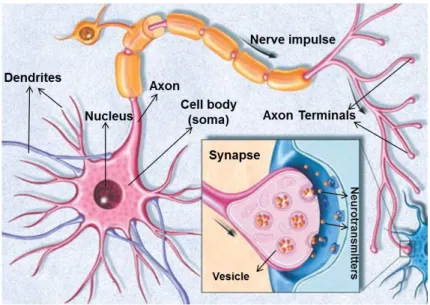
As shown in Fig.1.6, a neuron consists of three main parts- a cell body called the soma, the dendrites, and the axon. Dendrites are filaments that arise from the soma branching multiple times. The cell body (soma) is the metabolic center of the cell and it contains the cell nucleus. The nucleus stores the genes of the neuron. Dendrites act as the receivers for incoming signals from other nerve cells. The axon is the main
1.2 Neurobiology Basics
Figure 1.5: Species with increasing intelligence, number of neurons and synapses. Neuron and synapse numbers extracted from [22], [23], [24], [25], [26].
Figure 1.6: Illustration showing the basic structure of a neuron cell. Inset shows a zoom of the biological synapse. Adapted and modified from [27].
1. BACKGROUND
conducting unit, extruding from the soma, that is responsible for carrying electrical signals (called as action-potentials or spikes) to other neurons.
The spikes are rapid, transient, all-or-none nerve impulses, with an amplitude of 100 mV and a duration of about 1 ms (Fig.1.8). The neuron is surrounded by a plasma-membrane, made up of bilayer phospholipid molecules. The bilayer molecules make the membrane impermeable to the flow of ions. The impermeable membrane gives rise to a potential-gradient across the neuron and its extra-cellular medium due to differential ionic concentrations. In the unperturbed or equilibrium state, the neuron membrane stays polarized at a resting value of -70 mV [21]. However, the membrane is embedded with two special protein structures: namely ion-pumps, and voltage gated ion-channels, that allow the flow of ions in and out of the neuron under specific conditions. Ions such as Na+, K+, Cl− and Ca2+, play an essential role in the generation and propagation of the action-potentials.
Synapse is the region where the axon-terminal of one neuron comes close to the start of the dendrites of another neuron (see inset of Fig.1.6). Functionally, the synapse acts as a complex communication channel or the conductance medium between any two neurons, through which neuron signals are transmitted. The neuron which sends the spike to a synapse is termed as the pre-synaptic neuron, while the one that receives the spike is called the post-synaptic neuron. A single neuron in the cerebellum can have about 103 - 104 synapses, thus leading to massive parallel connectivity in the brain. Synapses and synaptic transmission can be either chemical or electrical in nature.
Electrical synapses are faster compared to chemical synapses. The signal trans-mission delay for electrical synapses is about 0.2 ms, compared to 2 ms for chemical synapses [28]. Electrical synapses are common in neural systems that require fast response time, such as defensive reflexes. An electrical synapse is a mechanical and electrically conductive link between two neurons that is formed at a narrow gap be-tween the pre- and post- synaptic neurons known as a gap junction. Unlike chemical synapses, electrical synapses do not have gain. The post-synaptic signal is either of the same strength or smaller than the original signal.
Chemical synapses allow neurons to form circuits within the central nervous system that are crucial for biological computations that underlie perception and thought. The process of chemical synaptic transmission is summarized in Fig.1.7. The process begins with the action potential traveling along the axon of the pre-synaptic neuron, until it
1.2 Neurobiology Basics
Figure 1.7: Illustration showing the chemical synaptic transmission process. Adapted and modified from [27].
reaches the synapse. Electrical depolarization of the membrane at the synapse leads to opening of ion-channels that are permeable to calcium ions. Calcium ions flow inside the pre-synaptic neuron, rapidly increasing the Ca2+ concentration. The high calcium
concentration activates calcium-sensitive proteins attached to special cell structures (called vesicles) that contain chemical neurotransmitters. The neurotransmitters are then released into the synaptic cleft, the narrow space between the membranes of the pre- and post-synaptic neurons. The neurotransmitter diffuses within the cleft and binds to specific receptor molecules located in the post-synaptic neuron membrane.
Binding of neurotransmitter activates receptor sites of the post-synaptic neuron. Activation of receptors may lead to opening of ion-channels in the postsynaptic cell membrane, causing ions to enter or exit the cell, thus changing the resting membrane potential. The resulting change in the membrane voltage is defined as post-synaptic potential (PSP). If the PSP depolarizes the membrane of the post-synaptic neuron, it is called an Excitatory Post Syanptic Potential (EPSP). While, if the PSP hyperpolar-izes the cell membrane, it is defined as an Inhibitory Post Synaptic Potential (IPSP). Depending on the type of PSP that a synapse generates, it can be classified as an excitatory- or inhibitory- synapse.
A neuron constantly integrates or sums all the incoming PSPs, that it receives at its dendrites, from several pre-synaptic neurons. The incoming EPSPs and IPSPs lead
1. BACKGROUND
Figure 1.8: (a) Illustration of neuron Action-Potential (spike). (b) EPSP and IPSP, adapted from [29].
to a change in the resting potential of the membrane. When the membrane potential depolarizes beyond -55 mV, it leads to spiking or action potential generation inside the post-synaptic neuron. Thus, a neuron would spike only if the following criteria is satisfied by eq.1.1
Σ(EPSP) − Σ(IPSP) > (−55mV ) (1.1)
Fig.1.8 shows that if the resultant stimuli at the post-synaptic neuron is less than the firing threshold (-55 mV), it leads to a failed initiation and no spike. In case of a failed initiation, the ion-pumps and the voltage gated ion-channels restore the membrane potential back to the resting value of -70 mV. An interesting attribute of synaptic transmission is that it has been shown to be stochastic in nature due to probabilistic release of neurotransmitters [30].
1.2.2 Synaptic Plasticity and STDP
The strength (or weight) of a synapse is defined by the intensity of change that it can induce in the membrane potential of a post-synaptic neuron. Within a neural net-work synaptic strength may differ from one synapse to another, and evolve with time, depending on the nature of stimuli. The ability of a synapse to change its strength, in response to neuronal stimuli is defined as synaptic plasticity. Increase of synap-tic strength is defined as synapsynap-tic-potentiation, while decrease is defined as synapsynap-tic-
synaptic-1.2 Neurobiology Basics
depression. Synaptic plasticity effects, can either be shortterm (lasting for few seconds to minutes) or long-term (few hours to days). Different underlying mechanisms such as- changes in the quantity of released neurotransmitters, and changes in the response activity of the receptors, cooperate to achieve synaptic plasticity. Plasticity effects in both excitatory and inhibitory synapses have been linked to the flow of calcium ions [31].
Learning and memory are believed to result from the effects of long-term synaptic plasticity such as long-term depression (LTD) and long-term potentiation (LTP)[32]. Both LTP and LTD are governed by multiple mechanisms that vary by species and the region of the brain in which they occur. In LTP the enhanced communication is predominantly carried out by improving the post-synaptic neuron’s sensitivity to signals received from the pre-synaptic neuron. LTP increases the activity of the existing receptors, and the total number of receptors on the post-synaptic neuron membrane. While, LTD is thought to result mainly from a decrease in post-synaptic receptor density [33]. Conventionally, synaptic plasticity has been understood and formulated to be bi-directional, continuous, finely graded or analog levels of synaptic conductance states [34]. However recent neurobiological studies [35], indicate that bi-directional synaptic plasticity may be composed of discrete, non-graded and more digital or binary-like (all or none) synaptic conductance states [36].
Spike-timing dependent plasticity (STDP) is a biological process or learning-rule that adjusts the efficacy of synapses based on the relative timing of spiking of the pre-and post-synaptic neurons. According to STDP, if the pre-synaptic neuron spikes be-fore the post-synaptic neuron, the synapse is potentiated. Whereas if the post-synaptic neuron spikes before the pre-synaptic neuron, the synaptic connection is depressed or weakened (LTD) [38]. Fig.1.9 shows the experimentally observed classical anti-symmetric STDP rule in cultured hippocampus neurons [37]. Note that the relative change of synaptic strength is more profound if the time difference (∆t) between the spikes is smaller. As ∆t increases, the effect of LTD and LTP becomes less profound like an exponential decay. STDP may vary depending upon the type of synapse and the region of the brain [39]. For classical anti-symmetric STDP rule, the width of the temporal windows for LTD and LTP are roughly equal in hippocampal excitatory synapses, whereas in the case of neocortical synapses the LTD timing window is con-siderably wider [40]. For some synapses [41], the STDP timing windows are inverted
1. BACKGROUND
Figure 1.9: Experimentally observed, classical anti-symmetric STDP rule, in cultured hippocampus neurons. ∆t < 0 implies LTD while ∆t > 0 implies LTP [37]. Change in EPSP amplitude is indicative of change in synaptic strength.
compared to the form of STDP shown in Fig.1.9. Different forms of symmetric-STDP rules have also been shown in literature [42].
1.2.3 Retina: The Natural Visual Processing System
Fig1.10, shows an anatomical diagram of the retina and the signal pathway for visual stimuli. Light stimuli (photons) is first converted into electrical signals and then to a sequence or train of action potentials (spikes) at the output of the retina. The retina consists of three major types of neuron cells; (i) photoreceptors (rods and cones), (ii) intermediate-neurons (bipolar, horizontal and amacrine), and (iii) ganglion cells. Light is first converted into electrical signals, through complex biochemical processes, occurring inside the rods and cones. The rods are mainly responsible for night time vision, have a high sensitivity to light and high amplification. The cones are primarily responsible for color vision, more suited for day-time, are less sensitive to light, and have lower amplification [32].
The electrical signals generated at the photoreceptor cells are passed to the intermediate-neurons (bipolar, horizontal and amacrine cells) through synaptic connections. The intermediate-neurons then pass the signals to the ganglion cells. The amacrine, bipolar
1.2 Neurobiology Basics
Figure 1.10: (a) Illustration showing different types of cells in the retina (b) Anatomical diagram of visual stimuli signal pathway starting at the photoreceptors and ending at the optic-nerve. Adapted from [32].
1. BACKGROUND
Figure 1.11: Pathway from the retina through the LGN of the thalamus to the primary visual cortex in the human brain [32].
and horizontal cells combine signals from several photoreceptors in such a way that the electrical responses evoked in ganglion cells depend critically on the precise spatial and temporal patterns of the light that stimulates the retina [32]. The retina compresses visual information by a factor of 100, as the number of photoreceptor cells is approxi-mately 100 million while the number of nerve fibers comprising the optic nerve is only one million.
The ganglion cells are responsible for producing the final output of the retina and their axons converge to the optic nerve. Based on the type of ganglion cell, there can be different output spike patterns for a given stimuli. The spatial region inside which a ganglion cell is sensitive to any stimuli is defined as its receptive-field. For most ganglion cells the receptive field is divided into two parts: a circular zone at the center, called the receptive field center, and the remaining area of the field, called the surround. ON-type ganglion cells fire frequently if their receptive field center is illuminated, while OFF-type ganglion cells fire frequently only if their receptive field surround is illuminated. In Fig.1.10b, the ganglion cell G1 is OFF-type, while G2 is ON-type.
The optic nerve conducts the output spike trains from the ganglion cells to the region known as lateral geniculate nucleus (LGN) of the thalamus. The LGN acts as the relay station between the retina and the visual cortex (Fig.1.11). The visual
1.2 Neurobiology Basics
cortex is one of the most studied and well-understood cortical system in primates. It consists of several layers; V1, V2 etc. Information inside the visual cortex is propagated in a hierarchical manner mainly in one direction (‘Feedforward’) [11]. Functionally, the neurons in the layer V1 respond as highly selective spatiotemporal filters. Their receptive fields can be typically modeled by Gabor filters [43], which are sensitive to spatial and temporal orientation (or movement). The neurons of the second layer (V2) are functionally responsible for higher tasks such as encoding of complex shapes, combination of directions, edge detection, and surface segmentation [44].
Synaptic plasticity and STDP are believed to play an important role in the learning of complex intermediate features in visual data in an unsupervised manner [45]. It has been shown [46] that receptor fields similar to the ones found in V1 can emerge naturally through STDP on sufficiently large visual stimuli.
1.2.4 Cochlea: The Natural Auditory Processing System
The human ear can be broadly divided in three regions (outer-, middle- and inner-ear). Hearing starts with the capture of sound in the outer-ear (Fig.1.12a). Sound waves and mechanical energy flow through the middle-ear to the inner-ear (cochlea), where it is transduced in to electrical neural signals and coding. The complex auditory pathways of the brain stem mediate certain functions, such as the localization of sound sources, and forward auditory information to the cerebral cortex. Several distinct brain areas analyze sound to detect the complex patterns characteristic of speech.
The human cochlea consists of coils with progressively diminishing diameter, stacked in a conical structure like a snail’s shell. The interior of the cochlea contains three fluid-filled tubes, wound helically around a conical bony core called the modiolus. In a cross-sectional view (Fig.1.12b), the uppermost fluid-filled tube is the scala-vestibule, the middle tube is scala-media, and the lowermost tube is called the scala-tympani. A thin membrane (Reissner’s membrane) separates the media from the scala-vestibuli. The basilar membrane, which forms the partition between the scala-media and the scala-tympani, is a complex structure where the transduction of auditory-to-electrical signals occurs.
The basilar membrane acts as a mechanical analyzer of sound frequencies. Its mechanical properties vary continuously along the cochlea’s length. As the cochlear chambers become progressively larger from the organ’s apex toward its base the basilar
1. BACKGROUND
Figure 1.12: (a) Illustration of the human ear and (b) cross-section of the cochlea, adapted from [29].
Figure 1.13: (a) Illustration of uncoiled basilar membrane with different frequency sen-sitive regions, adapted from [47](b) inner hair cell, movement of the stereocilium leads to generation of receptor potentials, adapted from [29]
1.2 Neurobiology Basics
Figure 1.14: (a) Illustration showing the organ of corti in the cochlear cross-section. (b) zoomed view of the organ of corti showing location of the inner hair cells, adapted from [21]
membrane decreases in width. The membrane is relatively thin and floppy at the apex of the cochlea but thicker and tauter towards the base. Such variation in mechanical properties accounts for the fact that the basilar membrane is tuned to a progression of frequencies along its length [21]. At the apex of the human cochlea the partition re-sponds best to the lower frequencies of the order of 20 Hz, while at the opposite end, the membrane responds to higher frequencies around 20 kHz (Fig.1.13a). The relation be-tween characteristic frequency and position upon the basilar membrane varies smoothly and monotonically but is not linear. Instead, the logarithm of the best frequency is roughly proportional to the distance from the cochlea’s apex.
The organ of Corti is an important receptor part of the inner ear. It extends as an epithelial ridge along the length of the basilar membrane (Fig.1.14). It contains approximately 16,000 hair cells innervated by about 30,000 afferent nerve fibers, which carry information into the brain along the eighth cranial nerve. Like the basilar mem-brane, both the hair cells and the auditory nerve fibers are tonotopically organized: At any position along the basilar membrane they are optimally sensitive to a particular frequency, and these frequencies are logarithmically mapped in ascending order from the cochlea’s apex to its base. The organ of Corti contains two types of hair cells (Fig.1.13b). The inner hair cells form a single row of approximately 3500 cells. Farther from the helical axis of the cochlear spiral lie rows of about 12,000 outer hair cells [21]. When the basilar membrane vibrates in response to a sound, the organ of Corti is also carried with it. This leads to deflection of hair bundles (Fig.1.13a). The
me-1. BACKGROUND
chanical deflection of the hair bundle is the stimulus that excites each hair cell of the cochlea. This deflection leads to generation of receptor potentials. The receptor poten-tials of inner hair cells can be as great as 25 mV in amplitude. An upward movement of the basilar membrane leads to depolarization of the cells, whereas a downward de-flection leads to hyperpolarization. Due to the tonotopic arrangement of the basilar membrane, every hair cell is most sensitive to stimulation at a specific frequency. On average, successive inner hair cells differ in characteristic frequency by about 0.2%. In-formation flows from cochlear hair cells to neurons whose cell bodies lie in the cochlear ganglion. Since this ganglion follows a spiral course within the bony core (modiolus) of the cochlear spiral, it is also called the spiral ganglion(Fig.1.14). About 30,000 ganglion cells connect the hair cells of each inner ear. Each axon connects a single hair cell, but each inner hair cell directs its output to several nerve fibers, on average about 10. This arrangement has important consequences. Firstly, the neural information from which hearing arises originates almost entirely at inner hair cells, which dominate the input to cochlear ganglion cells. Secondly, the output of each inner hair cell is sampled by many nerve fibers, which independently encode information about the frequency and intensity of sound.
Each hair cell therefore forwards information of somewhat differing nature to the brain along separate axons. Finally, at any point along the cochlear spiral, or at any position within the spiral ganglion, neurons respond best to stimulation at the characteristic frequency of the contiguous hair cells. The central nervous system can get information about sound stimulus frequency in two ways. Firstly, a spatial code; the neurons are arrayed in a tonotopic map such that position is related to characteristic frequency. Secondly, a temporal code; the neurons fire at a rate reflecting the frequency of the stimulus.
1.3
Simplified Electrical Modeling
Numerous models of biological neurons and synapses, with varying degrees of com-plexity and abstraction, exist in literature. The comcom-plexity and the choice of a model depends on the application. For better understanding the working of the biological neurons or to simulate biology it is essential to have a detailed model which takes in
1.3 Simplified Electrical Modeling
Figure 1.15: (a) Simplified circuit equivalent of the Hodgin-Huxley (HH) neuron model. (b) Circuit model with synapses as variable programmable resistors [49].
account the dynamics at the level of individual ion-channels and underlying biophys-ical mechanisms. While for the purpose of bio-inspired or neuromorphic computing, which is more closely related to the scope of the work presented in this thesis, simple behavioral models are sufficient.
One of the earliest and simplest neuron models is the Integrate-and-Fire (IF) neuron model shown as early as 1907 [48]. In this model a neuron is represented by a simple capacitive differential
eq.1.2-I(t) = Cm·
dVm
dt (1.2)
Where, Cm denotes the neuron membrane capacitance. According to the IF model,
the neuron constantly sums or integrates the incoming pre-synaptic currents and fires (generates action potential) when the membrane voltage reaches a certain firing thresh-old voltage (Vth). An advanced and more relevant form of the IF model is the
Leaky-Integrate-and-Fire (LIF) model, described by the eq.1.3-I(t) − Vm(t)
Rm
= Cm·
dVm(t)
dt (1.3)
The LIF model takes in account the leakage-effect of the neuron membrane potential by drift of some ions, assuming that the neuron membrane is not a perfect insulator. Rm
denotes the membrane resistance. For the neuron to fire, the accumulated input should exceed the threshold Ith>Vth/Rm. Several CMOS-VLSI hardware implementations of
1. BACKGROUND
A more detailed model is the Hodgkin-Huxley neuron model (HH). It describes the action potential by a coupled set of four ordinary differential equations [51]. Fig.1.15a, shows the simplified circuit equivalent of the HH model. The bilayer phospholipid membrane is represented as a capacitance (Cm). Voltage-gated ion-channels are
rep-resented by nonlinear electrical conductances (gn, where n is the specific ion- channel
for Na+, K+), the conductance is a function of voltage and time. The electrochemical gradients driving the flow of ions are represented by batteries (En and EL). Ion-pumps
are modeled by current sources (Ip). Interestingly, neurons have also been modeled
as pulse frequency signal processing devices, and synapses as variable programmable resistors (Fig.1.15b) [49].
1.4
Nanoscale Hardware Emulation of Synapses
Several different hardware embodiments of artificial neural networks exist in literature. In this section we summarize some state-of-art hardware implementations of synapses based on (i) VLSI-technology and (ii) Exotic devices. We outline some limitations of these approaches and introduce the concept of emerging non-volatile Resistive Memory (RRAM) technology and its advantages. The underlying or unifying theme in most of the embodiments discussed in this section is that the synapse is broadly treated as a non-volatile, programmable resistor.
1.4.1 VLSI-technology
These include emulation of synaptic behavior with VLSI structures such as floating-gate transistors, DRAM and SRAM.
1.4.1.1 Floating-gate Synapses
The 10240 synapses in Intels ETANN chip were realized using EEPROM cells (see Fig.1.16) [8]. For each synapse circuit in ETANN, a pair of EEPROM cells are in-corporated in which a differential voltage representing the weight may be stored or adjusted. Electrons are added to or removed from the floating gates in the EEPROM cells by Fowler-Nordheim tunneling. A desired differential floating-gate voltage can be attained by monitoring the conductances of the respective EEPROM MOSFETs.
1.4 Nanoscale Hardware Emulation of Synapses
Figure 1.16: Intel ETANN synapse structure implemented using EEPROM floating-gate devices [8].
Figure 1.17: (a) Layout of poly silicon floating-gate synaptic device [52]. (b) ciruit schematic of floating-gate synapse with transconductance amplifier [52]. (c) layout of floating-gate pFET synaptic device [53].
1. BACKGROUND
Figure 1.18: (a) circuit schematic of analog DRAM based synapse with three additional transistors [55]. (b) circuit schematic of DRAM based synapse with transconductance amplifier [56].
Double-poly floating gate transistors along with transconductance amplifiers (Fig.1.17a,b) were used by Lee et. al [52], for implementing VLSI synapse circuits. In this approach the synaptic weight was programmed using Fowler-Nordheim tunneling, and the neural computation is interrupted for the duration of the applied programming voltages. Cor-relation learning rules have also been demonstrated on synapses made of floating-gate pFET type structures, as shown in Fig.1.17c, [53]. In this approach Fowler-Nordheim tunneling is used to remove charge from the floating-gate and thus increase the synapse channel current. Conversely, pFET hot-electron injection is used to add charge to the floating-gate and decrease the synapse channel current. More recently synaptic plastic-ity effects like LTP/LTD and the STDP learning rule were demonstrated on floating-gate pFET structures with the help of additional pre-synaptic computational circuitry [54].
1.4.1.2 Dynamic Random Access Memory (DRAM) or Capacitive Synapses Different DRAM (or capacitor based) synaptic hardware implementations utilizing both analog and digital types of storage have been proposed in literature. Jerzy et.al, demon-strated an analog multilayer perceptron network with back-propagation algorithm using nonlinear DRAM synapses [55]. Their synapse consists of a storage capacitor and 3 additional transistors (Fig.1.18a).
The DRAM based analog synaptic weight storage suffers from capacitive discharge, need for frequent refresh, noise induced from the switching transistors and errors due to clock feedthrough [55]. Lee et.al, proposed a DRAM based synapse with 7 additional
1.4 Nanoscale Hardware Emulation of Synapses
Figure 1.19: Capacitor based synapse with additional learning and weight update circuit blocks [58].
transistors or a transconductance amplifier (Fig.1.18b). They show a 8-bit synaptic weight accuracy with a 0.2 s refresh cycle. Additional decoder circuitry is required to program the synapse weight voltage. Takao et.al, demonstrated a digital chip architec-ture with 106 synapses [57]. They use an on-chip DRAM cell array to digitally store 8-bit synaptic weights with automatic refreshing circuits. In some capacitive imple-mentations there are additional weight update circuits inside the synaptic block, like the one shown in Fig.1.19, [58]. The additional circuits are needed to implement the learning rules. Similar of circuits with learning functionality are also shown in [59], [50].
1.4.1.3 Static Random Access Memory (SRAM) Synapses
More recently, the use of standard and modified SRAM cells has also been proposed for synaptic emulation. IBM proposed a modified 8-T transposable SRAM cell (Fig.1.20) in their digital neurosynaptic core [60]. Their modified 8-T structure enables single-cycle write and read access in both row and column directions. The cell area is 1.6 µm2 in 45 nm node. The 8-T SRAM synapses have binary weights which are probabilistically controlled. A variant structure containing 4-bit analog weight was also implemented [60].
4-bit SRAM cells are also used to store individual synaptic weights in the wafer-scale FACETS neuromorphic project [61]. Fig.1.21 shows the schematic diagram of a single synapse for the FACETS project. Two types of plasticity rules: short-term depression (STD) and STDP are implemented using the FACETS synapses.
1. BACKGROUND
Figure 1.20: IBM’s 45 nm node neurosynaptic core and 8-T transposable modified SRAM cell [60].
Figure 1.21: Synapse schematic comprising of 4-bit SRAM cells for the wafer-scale FACETS neuromorphic project [61].
1.4 Nanoscale Hardware Emulation of Synapses
The Spinnaker approach uses specially designed hardware synaptic channels with off-chip mobile DDR SDRAM memory with a 1 GB capacity. Synaptic weights use a large, concurrently-accessed global memory for long-term storage. Since the SDRAM resides off-chip, it is easy to expand available global memory simply by using a larger memory device [62].
1.4.1.4 Limitations of VLSI type synapses
While synaptic emulations that use VLSI constituents discussed in the previous sec-tion (like floating-gate transistors, DRAMs, SRAMs, DDR-SDRAM) are tempting to use, considering the availability of standardized design tools and a mature fabrication process, their exist several limitations. Floating-gate devices are not ideal for map-ping bio-inspired learning rules because unlike biological synapses they are 3-terminal. During synaptic learning individual synapses may undergo weight modification asyn-chronously, which is not very easy to do with the available addressing schemes for large Flash arrays. Floating-gate devices also require high operating voltages. In many cases, additional pre-synaptic circuitry is required to implement timing dependent learning rules, due to the difference in the charging and discharging physics of the floating gate devices. The pulse shapes used to program floating-gate devices are complicated. En-durance of even state-of-the art floating-gate devices (Flash) is not very high. Due to the operating physics, there exists an inherent limitation on the frequency of program-ming synapses based on floating-gate FETs.
The DRAM or capacitor based synapses require frequent refresh cycles to retain the synaptic weight. In most of the capacitor based demonstrations, a single synapse circuit needs more than 10 additional transistors to implement learning rules, as shown in sec.1.4.1. The capacitor is also an area consuming entity for the circuit. The SRAM based synapses further suffer due to disadvantage in terms of area consumption and volatility. When the network is turned off, the synaptic weights are lost, and so they need to be stored to some offline memory during or after the learning. Reloading of the synaptic weights during learning operation will lead to additional power dissipation and silicon area overhead. These limitations lay the basis for the interest in synaptic emulation with new types of emerging non-volatile memory technology (RRAM) as described in sec.1.4.3.
1. BACKGROUND
1.4.2 Exotic Device Synapses
Several interesting exotic devices such as organic-transistors, single-electron transistors, optically-gated transistors, atomic-switches and even thin-film transistors have been used to implement synaptic behavior.
Alibart et. al, propose an organic nanoparticle field-effect transistor (NOMFET) that can emulate effects such as synaptic short-term plasticity effects (potentiation/depression) and STDP based learning rules [63]. The NOMFET structure (Fig.1.22a) exploits (i) the transconductance gain of the transistor and (ii) the memory effect due to charges stored in the nano-particles (NPs). The NPs are used as nanoscale capacitors to store the electrical charges and they are embedded into an organic semiconductor layer of pentacene. The transconductance of the transistor can be dynamically tuned by the amount of charge in the NPs. More recently the NOMFET based synapses were also used to demonstrate associative learning based on Pavlov’s dog experiment [64].
A.K Friesz used SPICE models to propose a carbon nanotube based synapse cir-cuit (Fig.1.22b) [65]. The output of their CNT synapse circir-cuit produces excitatory post-synaptic potentials (EPSP). Carbon nanotube transistors with optically controlled gates (OG-CNTFETs) have also been proposed by different groups for synaptic em-ulation (see Fig.1.22c,d) [66], [67]. Agnus et.al [67], show that the conductivity of the OG-CNTFETat can be controlled independently using either a gate potential or illumination at a wavelength corresponding to an absorption peak of the polymer.
Recently, 2-terminal ”atomic switch” structures consisting metal electrodes, a nanogap and an Ag2S electrolyte layer (see Fig.1.23a), have been shown to emulate short-term
synaptic plasticity and LTP type of effects [68], [69]. Avizienis et. al, [70] fabricated massively interconnected silver nanowire networks (Fig.1.23b) functionalized with in-terfacial Ag/Ag2S/Ag atomic switches. Cantley et.al, used spice models to demonstrate
hybrid synapse circuits comprising of nano-crystalline ambipolar silicon thin-film tran-sitors (TFT) and memristive devices [71].
The exotic devices discussed herein suffer from limitations such as complicated fabrication process, poor CMOS compatibility, low technological maturity, and high voltage operation in some cases.
1.4 Nanoscale Hardware Emulation of Synapses
Figure 1.22: (a) Physical structure of the NOMFET. It is composed of a p+ doped bottom-gate covered with silicon oxide (200 nm). Source and drain electrodes are made of gold and Au NPs (20 nm diameter) are deposed on the interelectrode gap (5 µm), before the pentacene deposition [64]. (b) The carbon nanotube synapse circuit [65]. (c) Neural Network Crossbar with OG-CNTFET synapse [66]. (d) Schematic representation of a nanotube network-based OG-CNTFET [67].
1. BACKGROUND
Figure 1.23: (a) Schematics of a Ag2S atomic switch inorganic synapse. Application
of input pulses causes the precipitation of Ag atoms from the Ag2S electrode, resulting
in the formation of a Ag atomic bridge between the Ag2S electrode and a counter metal
electrode. When the precipitated Ag atoms do not form a bridge, the inorganic synapse works as STP. After an atomic bridge is formed, it works as LTP [68]. (b) SEM image of complex Ag networks produced by reaction of aqueous AgNO3with (inset) lithographically
patterned Cu seed posts [70].
1.4.3 Resistive Memory Technology (RRAM)
Resistive random access memory (RRAM) is an umbrella term for emerging non-volatile memory (NVM) devices and concepts based on electrically switchable resistance states. The motivation behind the development of RRAM technologies is to overcome the lim-itations of existing VLSI memory concepts. A RRAM cell is generally a capacitor-like MIM structure, composed of an insulating material ‘I’ sandwiched between two metal-lic electrodes ‘M’ [72]. The MIM cells can be electrically reversibly switched between two or more different resistance states by applying appropriate programming voltages or currents. The programmed resistance states are non-volatile. Based on the type of material stack and the underlying physics of operation, the RRAM devices can be classified in several categories. Fig.1.24, shows different types of emerging RRAM tech-nologies classified on the basis of the underlying resistance-switching physics. RRAM is also vaguely defined as ‘memristor’ or ‘ReRAM’.
This thesis focuses on three specific types of RRAM technologies: (i) unipolar Phase Change Memory (PCM), based on phase change effects in chalcogenide layers, (ii) bipolar Conductive Bridge Memory (CBRAM), based on electrochemical metallization effect, and (iii) bipolar Oxide based resistive memory (OXRAM), based on valency change/electrostatic memory effects.
1.4 Nanoscale Hardware Emulation of Synapses
Figure 1.24: Classification of the resistive switching effects which are considered for non-volatile memory applications [72].
1. BACKGROUND
Table 1.1: Comparison of emerging RRAM technology with Standard VLSI technologies. Adapted from ITRS-2012. (Values indicated for PCM and Redox are the best demon-strated.) Redox includes both CBRAM and OXRAM devices.
Parameter DRAM SRAM NOR
Flash NAND Flash PCM Redox (OX/CB) Cell Area 6F2 140F2 10F2 5F2 4F2 4F2 Feature Size (nm) 36 45 90 22 20 9 Read Time (ns) <10 0.2 10 50 12 <50 Write-Erase Time <10 ns 0.2 1 µs / 10 ms 1 ms / 0.1 ms 50 ns / 120 ns 0.3 ns Write Voltage (V) 2.5 1 12 15 3 0.6/-0.2 Read Voltage (V) 1.8 1 2 2 1.2 0.15 Write Energy (J)
5E-15 5E-16 1E-10 >2E-16 6E-12 1E-13 Endurance 64 ms NA >10 years >10 years >10 years >10 years
1.4 Nanoscale Hardware Emulation of Synapses
RRAM technologies offer interesting attributes both for replacing standard VLSI type memories and also for emulating synaptic functionality in large-scale silicon based neuromorphic systems (see Tab.1.1). Some promising features of RRAM are: full CMOS compatibility, cheap fabrication, high integration density, low-power operation, high endurance, high temperature retention and multi-level operation [73], [74], [75]. The two terminal RRAM devices can be integrated in 2D or 3D architectures with-selector device configuration (1 Transistor/Diode - 1 Resistor) or with-selector-free con-figuration (1 Resistor) [72]. The detailed RRAM working, and state-of-art synaptic implementations with RRAM devices is discussed in chapters 2 and 3.
1.4.3.1 Memistor Synapse (The father of Memristor or RRAM)
The memistor is one of the earliest electronic devices developed specially for emula-tion of synaptic funcemula-tionality in artificial neural networks. It was first proposed and demonstrated in 1960 [76], by Bernard Widrow and Ted Hoff (who later became one of the inventors of the microprocessor), used as synapse in their pattern classification ADALINE neural architecture [77]. Memistor is a three-terminal device, not to be con-fused with the two-terminal memristor first theoretically postulated by Leon Chua in 1971 [78], and later experimentally claimed by HP labs [79], rather it is a predecessor to both of them.
Memistor working is based on reversible electroplating reactions. Fig.1.25a, shows the photograph of Widrows memistor made of pencil led graphite and a supporting copper rod. Resistance is controlled (or programmed) by electroplating copper from a copper sulphate-sulphuric acid solution on a resistive substrate (graphite). Change in memistor conductance with application of plating current and a hysteresis effect is shown in Fig.1.25b. Fig.1.26a shows the original ADALINE neural architecture with a 3x3 memistor array and 1 neuron, developed in 1960. Fig.1.26b shows a more recent and compact version of the same. Inspired from widrow’s electroplating based memistor, a fully solid state memistor for neural networks was demonstrated in 1990 [80]. It is a 3-terminal device based on tungsten-oxide (WO3), Ni-electrodes and a
Al-gate Fig.1.27a. A voltage controlled, reversible injection of H+ ions in electrochromic thin films of WO3 is utilized to modulate its resistance. A hygroscopic thin film of
Cr2O3 is the source of H+ ions. The resistance of the device can be modulated over
1. BACKGROUND
Figure 1.25: (a) Photo of the constituents of the copper-sulphate based memistor device. (b) Characteristic programming curves showing hysteresis loop in the memistor devices, adapted from [76].
Figure 1.26: (a) Photo of the ADALINE architecture with 1 neuron and 3x3 memistor synapses [76]. (b) Recent photo of the ADALINE system containing memistors taken at IJCNN-2011.
1.5 Scope and approach of this work
Figure 1.27: (a) Cross-section schematic of the tungsten oxide based 3-terminal memistor. (b) Programming characteristics of the solid state memistor device, adapted from [80].
control voltage. Fig.1.27b shows the time-dependent programming characteristics of the solid-state memistors.
1.5
Scope and approach of this work
The work done in this PhD thesis focuses on the development of a complete ”synapse-solution” for using specific RRAM devices inside large-scale ultra-low power neuromor-phic systems.
The ”synapse-solution” comprises of different ingredients starting from individual devices, circuits, programming-schemes and learning rules. For each of the three RRAM technologies investigated in this work (i.e. PCM, CBRAM and OXRAM), we begin with investigating the basic working and characteristics of the devices. We then iden-tify what device characteristics can be directly used in a neural learning environment, and which ones are not usable. At the device level we identify some material and phys-ical characteristics that can be tuned or engineered to optimize the individual synaptic performance. At the architectural level, we propose specific connection topologies and detailed programming methodologies (Read, Write, Refresh) for building low-power neuromorphic systems. At the level of algorithms or learning we propose the use of simplified and optimized learning rules. Finally we demonstrate relevant applications such as complex auditory and visual pattern extraction/recognition. The overall strat-egy for developing a perfect hardware ”synapse-solution” should be of bi-directional nature (see Fig.1.28). The bottom-up approach begins with an individual synaptic device, while the top-down approach is more application centric.
1. BACKGROUND
Figure 1.28: Bi-directional strategy (Top-down + Bottom-up) adopted for the work presented in this PhD thesis. To develop the ideal ”synapse-solution” optimization and fine-tuning was performed at different levels such as architectures, learning-rules and programming-schemes.(BS: Binary Stochastic synapses).
1.6 Conclusion
1.6
Conclusion
In this chapter, we looked at some key motivations behind R&D in the field of neu-romorphic computing. We then summarized the main biological concepts relevant for the purpose of this work. In the last section of the chapter, we discussed several dif-ferent hardware implementations of synapses and the positioning of emerging RRAM technologies. The following chapters specifically focus on synaptic emulation using individual RRAM technologies (PCM, CBRAM and OXRAM).
“An experiment is something which everyone believes except the person who did it,
A simulation is something that no one believes... except the person who did it.”
2
Phase Change Memory Synapses
This chapter discusses how Phase Change Memory (PCM) technology can be used to emulate biological synapses in large-scale neuromorphic systems with low-power dissipation and easy to implement programming methodology.
2.1
PCM Working Principle
PCM devices consist of an active chalcogenide layer sandwiched between two metal electrodes. The working principle exploits reversible and nonvolatile phase-change phenomenon inside chalcogenide layers such as Ge2Sb2Te5 (GST). The high resistive
amorphous phase is usually defined as the RESET state, while the low-resistive crys-talline phase as the SET state. When a bias is applied across the two electrodes of the PCM, current flows through the metallic heater and the chalcogenide layer, causing joule-heating. Depending on the pulse-duration, fall-time edge, and the amplitude of the current flowing through the device, crystalline, amorphous, or partially crystalline and partially amorphous regions can be created inside the chalcogenide layer. If the chalcogenide layer is melted and quenched quickly, it does not get sufficient time to re-organize itself into a crystalline structure and thus amorphous regions are created. If the chalcogenide layer is heated, between the glass-transition and the melting temper-ature, for sufficiently long time it leads to crystallization [73]. Intermediate resistance states can also be obtained by tuning the programming conditions and controlling the volume of amorphous/crystalline volume fraction created inside the chalcogenide layer [73].

![Figure 1.7: Illustration showing the chemical synaptic transmission process. Adapted and modified from [27].](https://thumb-eu.123doks.com/thumbv2/123doknet/12858097.368390/26.892.253.694.220.492/figure-illustration-showing-chemical-synaptic-transmission-adapted-modified.webp)
![Figure 1.21: Synapse schematic comprising of 4-bit SRAM cells for the wafer-scale FACETS neuromorphic project [61].](https://thumb-eu.123doks.com/thumbv2/123doknet/12858097.368390/41.892.180.662.716.962/figure-synapse-schematic-comprising-sram-facets-neuromorphic-project.webp)
![Figure 1.24: Classification of the resistive switching effects which are considered for non-volatile memory applications [72].](https://thumb-eu.123doks.com/thumbv2/123doknet/12858097.368390/46.892.178.784.352.892/figure-classification-resistive-switching-effects-considered-volatile-applications.webp)
![Figure 1.26: (a) Photo of the ADALINE architecture with 1 neuron and 3x3 memistor synapses [76]](https://thumb-eu.123doks.com/thumbv2/123doknet/12858097.368390/49.892.154.698.737.976/figure-photo-adaline-architecture-neuron-x-memistor-synapses.webp)
![Figure 2.19: Write operations based on the simplified-STDP rule. For a specific PCM, G % denotes an increase in conductance (thus, partial crystallization of the device), while G → denotes no change in conductance [111].](https://thumb-eu.123doks.com/thumbv2/123doknet/12858097.368390/82.892.265.701.676.992/figure-operations-simplified-specific-increase-conductance-crystallization-conductance.webp)
![Figure 2.25: AER video data snapshot. Cars passing on a freeway recorded with the DVS- DVS-sensor described in [117]](https://thumb-eu.123doks.com/thumbv2/123doknet/12858097.368390/89.892.238.591.220.562/figure-video-snapshot-passing-freeway-recorded-sensor-described.webp)
