HAL Id: hal-01247896
https://hal.archives-ouvertes.fr/hal-01247896
Submitted on 23 Dec 2015
HAL is a multi-disciplinary open access
archive for the deposit and dissemination of
sci-entific research documents, whether they are
pub-lished or not. The documents may come from
teaching and research institutions in France or
abroad, or from public or private research centers.
L’archive ouverte pluridisciplinaire HAL, est
destinée au dépôt et à la diffusion de documents
scientifiques de niveau recherche, publiés ou non,
émanant des établissements d’enseignement et de
recherche français ou étrangers, des laboratoires
publics ou privés.
3D advanced integration technology for heterogeneous
systems
Pascal Vivet, Christian Bernard, Fabien Clermidy, Denis Dutoit, Eric
Guthmuller, Ivan-Miro Panadès, Gaël Pillonnet, Yvain Thonnart, Arnaud
Garnier, Didier Lattard, et al.
To cite this version:
Pascal Vivet, Christian Bernard, Fabien Clermidy, Denis Dutoit, Eric Guthmuller, et al.. 3D advanced
integration technology for heterogeneous systems. 3D Systems Integration Conference (3DIC), 2015
International, Aug 2015, Sendai, Japan. �10.1109/3DIC.2015.7334468�. �hal-01247896�
3D Advanced Integration Technology for
Heterogeneous Systems
Pascal Vivet, Christian Bernard, Fabien Clermidy, Denis Dutoit, Eric Guthmuller, Ivan-Miro Panadès, G. Pillonnet,
Yvain Thonnart, Arnaud Garnier, Didier Lattard, Amandine Jouve, Franck Bana, Thierry Mourier, Séverine Chéramy
Univ. Grenoble Alpes, CEA, LETI, MINATEC Campus, 38054 Grenoble, France
Abstract—3D integration technology is nowadays mature
enough, offering today further system integration using heterogeneous technologies, with already many different industrial successes (Imagers, 2.5D Interposers, 3D Memory Cube, etc.). CEA-LETI has been developing for a decade 3D integration, and have pursued research in both directions: developing advanced 3D technology bricks (TSVs, µ-bumps, Hybrid Bonding, etc), and designing advanced 3D circuits as pioneer prototypes. In this paper, a short overview of some recent advanced 3D technology results is presented, including some latest 3D circuit’s description.
Keywords— 3D, TSV, NoC, Active Interposer
I. INTRODUCTION
After the profound evolution of deep submicron technologies, we are facing today the wall of transistor shrinking. More Moore trend is facing severe difficulties: cost, variability, power density, timing uncertainties [1]. In order to pursue technology and design integration, More Than Moore technologies, such as 3D integration, are becoming more attractive. With 3D technologies, and so-called Through Silicon Vias (TSV), it is possible to stack various dies together. The 3D technologies are opening a full scope of new application possibilities, by integrating more devices from potentially different technologies (CMOS, MEMS, DRAMs, etc.). Full 3D can be envisaged by stacking vertically dies on top of each other’s or Interposers – also called 2.5D – by stacking horizontally dies onto silicon substrate. We present in this paper one exemple of each configuration, both developed at CEA-Leti: A two dies logic stack (“3DNoC”) and a smart interposer (“IntAct”).
II. HOMOGENEOUS COMPUTING FABRIC USING 3DNOC
A. 3D Architecture & circuit
For power efficient embedded applications, Network-on-Chip (NoC) has already proven to be an advanced communication infrastructure for the current “2D” many-core architectures. Based on structured packet based interconnect, NoC offers full modularity, scalability, high performance, and quality of service, compared to existing bus-based interconnect. For 3D-stacked circuits, 3D NoC, as a natural extension of current 2D NoC, is then a promising solution for increased modularity and scalability [2]. Even if 3D technology introduces new application possibilities, it also incurs VLSI design problems. For example, delivering a clock to each die and dealing with clock synchronization and clock
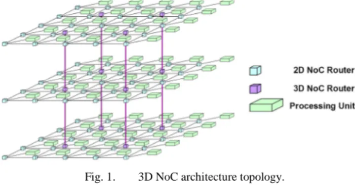
tree is a critical problem in the context of 3D circuits [3]. To avoid global clocking, Globally Asynchronous and Locally Synchronous (GALS) scheme must be adopted to implement efficiently a 3D NoC. In figure 1, a homogeneous asynchronous 3D NoC is proposed to build a 3D Multi-Core, using similar dies and tiles. The objective is to reduce mask costs, to improve yield by partitioning the multi-core system in smaller dies, while reducing the overall system consumption and latency, due to shorter NoC paths.
Fig. 1. 3D NoC architecture topology.
A Telecom baseband circuit, based on a 3DNOC, using 2 layers of identical dies, have been designed and fabricated in a 65nm technology in a Face2Back flip-chip assembly. The circuit implements some asynchronous 3D serial links [4].
B. Technology & Integration
For such a stacking and an application, 40µm pitch technology was required for die-to-die connection. A copper pillar process flow, 20µm diameter, Cu/SnAg (µbumps) and Cu/Ni/Au (copper post) metallurgy, was chosen for top – bottom die connection (figure 2) - A TSV-middle process, 10µm diameter and 80µm depth (Aspect ratio 8:1), and some copper pillar diameter 55µm, were chosen for die to package connection (figure 3). A face2Back flip chip assembly were needed, very similar to the one used for Wide I/O demonstrator [5].
Fig. 3. Cross section of the bottom die with TSV-middle and copper pillar diameter 55µm
One particularity of this stack is that both dies have strictly the same size. It makes impossible for the packaging to use capillary underfill, so that Non-Conductive Paste and thermo-compression process were used [6]. A cross section of the final package on BGA is shown on figure 4 and figure 5.
Fig. 4. Cross section of the final package, including 2 stacked dies
Fig. 5. Detail of the 3DNOC circuit stack
Packages are now available for final testing. More performance results will be submitted shortly.
III. ACTIVE INTERPOSER BASED MULTI-CORE SYSTEM
A. 3D Architecture & circuits
On one hand, since 3D technologies are currently not mature enough, stacking in 3D a large number (with #die>2) of homogenous logic dies is still not yet easily feasible (even if this is already done at product level for 3D memories). On the other hand, with Moore’s law for advanced nodes, the yield of large dies is constantly decreasing, which leads to prohibitive costs of high end large dies. One possible solution is to partition a large single die with low yield in smaller dies with better yield assembled in 2.5D using interposers [7]. More and more 3D players are forecasting the use of active logic within 2.5D interposers in order to further optimize the system, and justify the current high cost of passive interposers.
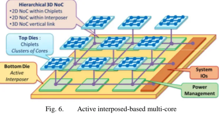
By splitting a multi-core system in multiple chiplets stacked onto an active interposer (figure 6), one can achieve: - Yield optimization: chiplets are composed of computing
processing units, fabricated in advanced technology, pre-tested and assembled on a large size interposer, fabricated in a mature technology. The active interposer logic density must obviously be kept low enough to maintain high yield of the large area active interposer, to preserve system cost.
Fig. 6. Active interposed-based multi-core
- Power & Thermal dissipation mitigation: compared to 3D thermal issues [8], power density is reduced, power delivery networks are simplified, and thermal dissipation is almost comparable to standard 2D dies.
- Smart Interposer features: by using active logic within the interposer, it is possible to integrate smart functions like high performance pipelined interconnects (NoC, PHYs), IO pads, Power Management, SoC infrastructure logic (Clock, Test, Debug), and Sensors (Stress, Thermal, etc). Compared to previous homogenous 3DNOC architecture, the system level interconnect is then hierarchical: 2D NoC within the chiplets to connect the clusters of cores, 2D NoC within the interposer to connect the chiplets, and 3D vertical links between the chiplets and the interposer. For 3D link throughput optimization, phase converters may be used [9]. For power management, by integrating switched capacitances on the interposer available area (without impact on interposer yield), a switch cap DC/DC converter avoids costly external passive components and provides efficient on-demand DVFS to individual chiplets [10].
A multi-core cache coherent architecture [11], integrating a total of 96 MIPS32 cores, including a fully cache coherent memory architecture, have been designed using FDSOI 28nm 22mm2 chiplets assembled on a 200mm2 CMOS 65nm active interposer, in a Face2Face chiplet interposer 3D assembly configuration. This demonstrator is named IntAct [12].
B. Technology & integration
Interposer technology has been introduced and then improved in the last few years [7]. Some electrical data has proven the feasibility of the integration, even if some challenges in terms of warp management, especially during final assembly, remains [13].
The specification for the demonstrator IntAct described in the first paragraph are nevertheless slightly different: first a very dense die-to-die interconnection matrix is needed for an optimized communication network between top and bottom dies. Pitch of 20µm or even less would open the door for higher performances. To obtain this fine pitch, 2 technologies are developed and evaluated.
First, copper pillar and µbumps limits are pushed to reach a pitch of 20µm (figure 7). Work on underfill is in parallel needed because current process of record is available with state of the art pitch of 40µm. Pre-applied underfill (non conductive paste and Wafer level underfill) can be used.
Fig. 7. µbumps Cu/SnAg diameter 10µm/pitch 20µm and its mettallurgy after reflow process.
To reach even more aggressive pitch and thus increase the possibility of partitioning between top & bottom dies, Cu-Cu direct bonding is also a very interesting alternative. This technology, based on almost standard CMP process, does not require any pressure and no temperature – No underfill is needed neither. If this technology is under development since several years and near of industrialization on a Wafer-To-Wafer approach, some advanced work on Chip-To-Wafer-To-Wafer is also under work, making this promising process compatible with interposer [14]. Crosse section of a pad stacked thanks to copper-copper direct bonding is shown on figure 8.
Fig. 8. Interconnection using Cu-Cu direct bonding
The second challenge of this demonstrator is warp management. Even if the interposer size is not too large (around 200mm²), stress management remains nevertheless a challenging topic in integration and particularly during 3D assembly. To limit the bow during wafer level and chip level process steps, simulation has proven that the first stress contributor is the silicon thickness. State of the art today for silicon thickness, driven by TSV aspect ratio, is a maximum thickness of 100 to 120µm.
Fig. 9. 10x120 µm TSV filled with Cu – excellent coverage of MOCVD TiN barrier
To increase the interposer thickness, very high aspect ratio of TSV is needed. Work on TSV, diameter 10µm, aspect ratio 12 and more, is on-going using alternative metal deposition, such as MoCVD or wet process (figure 9).
IV. CONCLUSION
3D architectures are now well known both from design and from technology aspects. The challenge now would be how to create smart system to optimize performances, industrialization, cost, time to market…Both examples in this paper aim different applications and finally design and technology bricks involved are very different and every choice need to be studied from the beginning to finally obtain the right 3D architecture. This emphasizes the need for a close common work between design & technology to obtain the best from 3D integration.
ACKNOWLEDGMENT
Authors would like to thank all its partners for their contribution in this work. Part of this work was funded thanks to the French national program “Programme d’Investissements d’Avenir, IRT Nanoelec” ANR-10-AIRT-05.
REFERENCES [1] IRTS roadmap http://www.itrs.net/
[2] A. Sheibanyrad, F. Petrot, A. Jantsch, “3D Integration for NoC-Based SoC Architectures”, Springer 2011, ISBN 978-1-4419-7617-8. [3] V. F. Pavlidis, I. Savidis, and E. G. Friedman “Clock Distribution
Networks for 3-D Integrated Circuits”, Proc. of IEEE Custom
Integrated Circuits Conference, CICC’08, 2008.
[4] P. Vivet, C. Bernard, E. Guthmuller, I. Miro-Panades, Y. Thonnart, F. Clermidy, “Interconnect Challenges for 3D Multi-cores:from 3D Network-on-Chip to Cache Interconnect”, ISVLSI’2015.
[5] P. Coudrain, J.P. Colonna, S. Chéramy & Al, “Towards Efficient and Reliable 300mm 3D Technology for Wide I/O Interconnects”, EPTC’2012
[6] A. Garnier, A. Jouve, R. Franiatte, S. Cheramy, « Underfilling Techniques Comparison In 3D CtW Stacking Approach”, ECTC’2014 [7] http://www.xilinx.com/support/documentation/white_papers/wp380_St
acked_Silicon_Interconnect_Technology.pdf
[8] C. Santos, P. Vivet, J.P. Colonna, P. Coudrain, R. Reis, “Thermal Performance of 3D ICs: Analysis and Alternatives”, 3DIC 2014. [9] J. Hilgemberg Pontes, P. Vivet, Y. Thonnart, “Two-phase Protocol
Converters for 3D Asynchronous 1-of-n Data Links”, ASP-DAC’15. [10] G. Pillonnet, N. Jeanniot, P. Vivet, « 3D ICs: An Opportunity for
Fully-Integrated, Dense and Efficient Power Supplies », 3DIC’2015. [11] E. Guthmuller, I. Miro-Panades, and A. Greiner, “Architectural
exploration of a fine-grained 3D cache for high performance in a manycore context”, VLSI-SoC 2013.
[12] S. Chéramy, F. Clermidy & Al, “The “active-interposer” concept for high-performance chip-to-chip connections”, Chip Scale Review, May-June 2014
[13] M. Sunohara, K. Miyairi & Al, “Electrical and morphological characterization for high integrated Silicon interposer and technology transfer from 200 mm to 300mm wafer”, ECTC 2013
[14] Y. Beillard, L.D. Cioccio, & Al, “Chip to wafer copper direct bonding electrical characterization and thermal cycling”, 3DIC 2013