HAL Id: lirmm-00433462
https://hal-lirmm.ccsd.cnrs.fr/lirmm-00433462
Submitted on 12 Sep 2019
HAL is a multi-disciplinary open access
archive for the deposit and dissemination of
sci-entific research documents, whether they are
pub-lished or not. The documents may come from
teaching and research institutions in France or
abroad, or from public or private research centers.
L’archive ouverte pluridisciplinaire HAL, est
destinée au dépôt et à la diffusion de documents
scientifiques de niveau recherche, publiés ou non,
émanant des établissements d’enseignement et de
recherche français ou étrangers, des laboratoires
publics ou privés.
Insertion Flow for Adaptive Compensation of
Variabilities
Bettina Rebaud, Marc Belleville, Edith Beigné, Christian Bernard, Michel
Robert, Philippe Maurine, Nadine Azemard
To cite this version:
Bettina Rebaud, Marc Belleville, Edith Beigné, Christian Bernard, Michel Robert, et al.. Digital
Timing Slack Monitors and their Specific Insertion Flow for Adaptive Compensation of Variabilities.
PATMOS: Power And Timing Modeling, Optimization and Simulation, Sep 2009, Delft, Netherlands.
pp.266-275, �10.1007/978-3-642-11802-9_31�. �lirmm-00433462�
J. Monteiro and R. van Leuken (Eds.): PATMOS 2009, LNCS 5953, pp. 266–275, 2010. © Springer-Verlag Berlin Heidelberg 2010
Digital Timing Slack Monitors
and Their Specific Insertion Flow
for Adaptive Compensation of Variabilities
Bettina Rebaud1,2, Marc Belleville1, Edith Beigné1, Christian Bernard1,Michel Robert2, Philippe Maurine2, and Nadine Azemard2
1
CEA, LETI, MINATEC, F38054 Grenoble, France {firstname.name}@cea.fr
2
LIRMM-CNRS - Universite Montpellier II, 34392 Montpellier, France
{firstname.name}@lirmm.fr
Abstract. PVT information is mandatory to control specific knobs to
compen-sate the variability effects. In this paper, we propose a new on-chip monitoring system and its associated integration flow, allowing timing failure anticipation in real-time, observing the timing slack of a pre-defined set of observable flip-flops. This system is made of specific structures located nearby the flip-flops, coupled with a detection window generator, embedded within the clock-tree. Validation and performances simulated in a 45 nm technology demonstrate a scalable, low power and low area, fine-grain system. The integration flow re-sults exhibit the weak impact of the insertion of this monitoring system toward the large benefits of tuning the circuit at its optimum working point.
1 Introduction
In order to face PVTA (Process Voltage Temperature Aging) variability issues [1-3], and to reduce design margins due to traditional corner-based methodologies, it is possible to reach the optimal operating point of the manufactured chip and thus, get rid of over-pessimism, in using dynamic adaptation of the circuit performances. This solution requires tunable knobs like programmable supply voltages, body biasing or scalable frequencies. In order to efficiently tune those parameters, a monitoring system, providing a real time and accurate diagnostic of the circuit has to be imple-mented. Two monitoring means have been proposed: (a) integrating specific non-functional structures or sensors [4-7]. (Those sensors can be difficult to calibrate, and are only sensitive to global variations) and (b) monitoring directly the sampling ele-ments of the chip (Latches or D-type Flip Flop) [8-12] to detect the occurrence of delay faults. Contrary to previous works, the second solution can detect local varia-tions and is much easier to use due to simple binary output data. On the other hand, to obtain good circuit coverage, many sensors have to be inserted. Solutions [8-10] pro-posed in line with this approach, i.e. solutions aiming at monitoring the critical paths, have several drawbacks like (a) short paths management imposing buffer insertion, (b) need of a replay or correction systems when an error is detected, (c) high timing
sensitivity to voltage or frequency scaling and process variations. [12] removes (a-b) disadvantages in suggesting anticipation before error occurrence. However, the pro-pounded implementation does not fit well with frequency or voltage scaling.
Within this context, the contribution of this work is to propose a new monitoring system in line with critical paths monitoring concept, aiming at improving existing implementations and anticipating timing violations over a wide range of operating conditions. The proposed system monitors locally, at run time, on one or more slow paths, critical timing slacks and discloses their evolution with PVT variations or age-ing phenomena. One key feature of the system consists in generatage-ing a detection win-dow directly using the clock tree architecture to distribute it efficiently to several sensors.
The paper is organized as follows: Section 2 presents the whole monitoring system features, its insertion close to the flip-flops and the specific structures. In section 3, the specific integration flow is detailed, applied with specific constraints. The section 4 provides simulation results of the whole system, validating the monitoring concept proposed.
2 Monitoring System Proposal
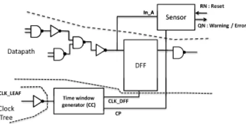
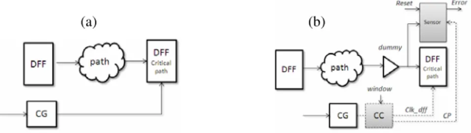
The proposed monitoring system (Fig.1) is composed of two blocks, designed as standard cell library elements: a sensor (Fig. 3) and a specific Clock-tree Cell (CC) (Fig. 4). The sensor is inserted close to the D-type Flip-Flops (DFF) located at the endpoints of critical timing paths of the design while, the CC are inserted within the associated clock leafs. Different cells sizing is proposed within the library allowing, if necessary, fine timing tuning.
Fig. 1. Proposed monitoring system implemented on a critical path endpoint As shown Fig.1 and 3, the sensor, acting as a stability checker, is directly con-nected to a data path output, i.e. to the DFF input. It also receives on one of its input the signal CP periodically provided by CC, which can drive several sensors. Edges of CP signal are in phase with those of the clock. The basic function of the sensor is to detect the occurrence of a full or partial transition of the signal In_A during the detec-tion window (of duradetec-tion Dpulse) posidetec-tioned in time by the rising edge of CP as shown Fig. 2. More precisely, this detection window starts at (In-to-CP + CLK_DFF) before the rising edge of the clock and ends at (In-to-CP + CP-to-CLK_DFF – Dpulse) due to some timing characteristics of both sensor and CC. A key
268 B. Rebaud et al.
point here is that (In-to-CP + CP-to-CLK_DFF - Dpulse) must be greater than, or at least equal to, the setup time (Tsetup) of the monitored DFF to detects timing warn-ings rather than timing errors. In-to-CP is a timing characteristic of the sensor due to its internal inverters [11], and CP-to-CLK_DFF the time interval separating the rising edges of CP and CLK_DFF.
Fig. 2. Transition detection chronogram
If a transition occurs within the detection window, the monitor latches an error sig-nal meaning that, during the last clock cycle, PVT conditions and the data processed by the monitored logic are such that the timing slack (before occurrence of a setup time violation) is lower than Tm = (In-to-CP + CP-to-CLK_DFF - Tsetup). Consider-ing those timConsider-ing characteristics, sensors are able to warn an imminent system timConsider-ing failure by detecting the occurrence of a signal transition within the detection window.
To tackle the complexity of actual embedded systems, made of various functional blocks with different levels of timing criticality or working under different operating conditions (Vdd, multiple clock domains), several clock tree cells CC (Fig. 4) gener-ating different time window widths Dpulse and thus, different guard margins Tm must be available in the specific standard cell library.
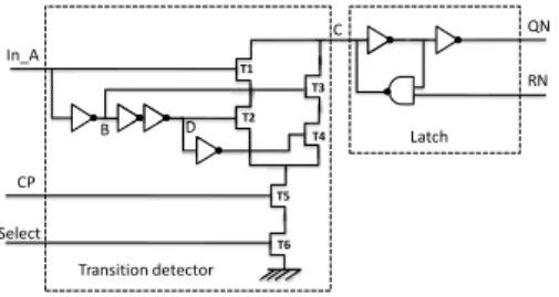
Fig. 3. This one-input sensor works with the load and the discharge of the C node. In order to
reduce the area, several transition detectors can share the same latch. In this condition, C is bigger and the structure slower: trade-off has to be made.
Performance and system validation results obtained considering a 45nm Low Power technology are given in [11]. Those results demonstrate that the implemented structures are robust to power supply, frequency and temperature variations. More precisely, it is shown in [11] that:
– the 4-input sensor can detect the occurrence of transitions until 0.6V @ 125C in worst case process, and has low process induced delay variations.
– the clock cell CC provides reliable detection window(s) whatever the environ-mental conditions are.
– the system can achieve interesting timing margin reduction (w.r.t. to worst case timing conditions). CLK_LEAF Delay D1 Delay D2 Delay D3 CLK_DFF CP Pulse generator n1 n2 n3 (a)
Fig. 4. Example of specific clock cell (CC) implementation
Sensor cells with 1 and up to 4 inputs and a programmable CC with W1 and W2 detection windows have been designed, layout drawn and characterized in 45nm Low Power technology, in order to create a new standard cell library. Sensors were charac-terized as DFF since their timing behavior is quite similar to that of DFF. The descrip-tion of CC was done accordingly to the descripdescrip-tion of any clock buffer.
3 Integration Flow
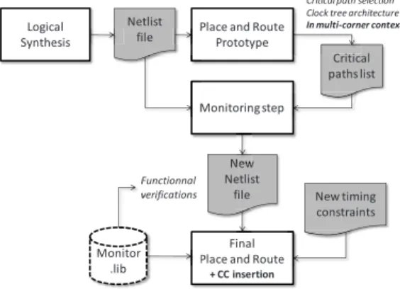
In order to demonstrate the whole system efficiency, in terms of functionality and integration easiness, a test chip has been designed, and a dedicated digital flow has been studied (Fig. 5). Further details on test chip are given section 4. This section aims at describing this specific flow, and the new timing constraints that must be taken into account for a generic block.
As shown Fig.5, three steps are required to integrate the proposed monitoring sys-tem. In a first step, a prototype (a placed and routed design) is obtained in order to identify the critical paths to be monitored, and to get an accurate description of the
Place and Route Prototype
Monitoring step
Final Place and Route
+ CC insertion Logical Synthesis Netlist file Critical paths list New Netlist file Functionnal
verifications New timing constraints Monitor
.lib
Critical path selection Clock tree architecture In multi-corner context
270 B. Rebaud et al.
clock tree. This step achieved, sensors and dummy cells are inserted in the netlist. Then, starting from the prototype results obtained from step 1, final place and route steps are performed, considering additional timing constraints related to CC and sen-sors insertion. In this last step, balancing the nets between DFF and their associated sensor is a key design guideline.
3.1 Critical Paths Choice
Getting an exhaustive coverage of our test chip is unrealistic as the numbers of sen-sors will double the occupied area and the power consumed by the sequential ele-ments. Thus, some critical paths to be monitored have to be selected.
One possible solution is to use Statistical Static Timing Analysis [13-14]. SSTA is performed to identify the paths (assuming that these paths are correlated enough) with the highest probabilities of violating the setup time constraint. However, with the decreasing transistor length and the increasing impact of local and random variations, correlations between timing paths shrink, leading to a growing number of paths that have to be monitored to remain sure to detect warning signal before a failure.
Therefore, another selection policy was adopted since our goal was to prevent a system failure before the occurrence of any timing violation (no timing error is al-lowed in the system). Considering this constraint, our strategy is to impose specific target slack constraints during the synthesis and the place and route steps. More pre-cisely, specific target slack constraints were chosen to create the set of pre-defined critical paths to be monitored. Specifically, we intentionally relax the target slack constraint of a set of critical paths. This set includes the worst critical path which has been identified during synthesis runs at worst case and tight timing constraints.
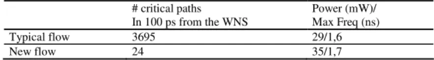
This results in a timing slack distribution characterized by two distinguishable sets of paths (illustration Table 1). A reduced set of paths characterized by a reduced tim-ing slack forms the set of paths to be monitored, and a huge set of paths characterized by larger timing slacks, and more precisely by slacks 100 ps greater than the most critical path (which is in the first set of paths).
Table 1. Number of critical path endpoints with a delay value lower than that of the worst
critical path by less than 100ps (synthesis step at worst timing corner 1,05V, 125°C)
# critical paths In 100 ps from the WNS Power (mW)/ Max Freq (ns) Typical flow 3695 29/1,6 New flow 24 35/1,7
Such timing slack distribution is obtained thanks either to multi-mode capabilities of CAD tools or to specific relaxing tool commands. However, it is of prime impor-tance to warrant that the paths to be monitored are representative of the circuit operat-ing in any possible conditions. Thus a verification step is required in order to fulfill this condition, using either multi-corner or statistical simulations. This specific flow results in over-constraining some paths from a timing point of view that consists mainly in increasing the power consumption as shown Tab.1. However, the overhead is expected to be significantly lower than the gains achieved by applying adaptive voltage, body-biasing and frequency scaling techniques.
3.2 Monitoring Step and Specific Place and Route Constraints
The monitoring phase is performed after the true critical paths identification, in all operating conditions, before the final place and route step. As shown Fig.5, the moni-toring phase aims at providing: (a) a new netlist file including dummy cells and sen-sors, as shown Fig. 6, and (b) a new timing constraints file to guide the place and route step. This step can be fully automated by developing specific scripts to ease the monitor integration. It is also possible to integrate some sensors such as they share several flip-flops; however this is highly dependent on the clock tree structure. As a result, 4 DFF sharing the same sensor has been found as a practical limit in our test-case.
Moreover, Clock Cells (CC) cannot be inserted during the monitoring phase since it would induce some setup and hold timing violations during functional verifications in locally modifying the clock skew. Furthermore, this specific point is highly critical if clock gating is applied to reduce the dynamic power consumption. As a result, the clock cell insertion is pushed to the next step.
Fig. 6. Critical path before (a) and after (b) the monitoring step. Sensors are added with specific
dummy cells allowing an easy place and route. Clock Cells are inserted later.
To ensure that no skew will appear between the event going to the sensor and the same one going to the DFF(s), and thus keep the Tm margin safe, specific timing constraints must fixed in the constraint file considered during the final place and route step. This timing specifications aim at constraining the timing driven place and route tool such as the timing fork between the DFF(s) and the related sensor remains well balanced. This can be done by imposing a specific timing constraint to the dummy cell driving the sensor and its associated DFF. Furthermore, additional hold time issues introduced by the CC detection window (when the window is still open after the rising clock edge) have also to be considered and fixed by adding some specific constraints in the timing constraint file. However, the reduced detection window width (compared to [8-10]) enables to insert a limited number of buffers in short paths.
3.3 Specific Clock Tree Cell Insertion
As the clock tree architecture may be highly sensitive to PVT variations, CC are in-serted as close as possible to the monitoring path endpoint (Fig. 7) thanks to the addi-tional timing constraints introduced at the monitoring phase. This method leads to
272 B. Rebaud et al.
– reduce the impact of spatial correlations on the timings of the different monitor-ing elements.
– limit the impact of local voltage drops and temperature gradients on timings. – reduce the impact on timings of interconnects variability.
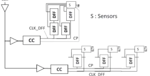
CC Sensor D Q DFF QN RN Sensor D Q DFF QN RN Sensor D Q DFF QN RN DFF DFF DFF S : Sensors S S S CP CLK_DFF CC DFF DFF DFF DFF S QN CP CLK CLK_DFF
Fig. 7. Final clock tree architecture example with two CC driving 7 DFF and 4 sensors As a result, Clock Cell insertion is performed at the Place and Route level, after a first clock tree synthesis (CTS). The insertion done, a second CTS is run in order to balance the tree, and minimize the global skew of the design before the final routing.
4 Results
This section describes the main results while using the dedicated flow (Fig. 5), by pointing out the new constraints efficiency and the validation of the monitoring sys-tem concept.
The monitoring system has been integrated in an arithmetic and reconfigurable block incorporating: 4 SRAMs, several register banks, and computing elements such as dividers or Multipliers-Accumulators (MAC). This block, inserted in a telecom SoC was considered as an ideal test case because of its timing criticality. Due to the complexity of the considered real time application, no replay of instruction sets was feasible at system level, and timing performances have to be high enough to satisfy a strained real time environment. Designed in 45nm STMicroelectronics Low Power technology, it contains about 13400 flip-flops, which leads to a 606*558 µm² core floorplan implementation. The timing constraint period is 1.5 ns with nominal process libraries, @ 25°C and 1,1V.
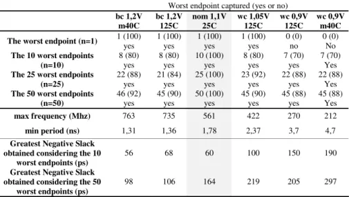
Critical path endpoint selection. Applying the specific flow on the placed and routed prototype, a set of 160 critical path endpoints, defining a set of critical paths, situated at the output of the first stage of the pipelined MAC, was isolated. The maximum operating frequency Fmax was characterized in nominal conditions. Values of 1.78 ns and 1.36 ns were estimated as the minimal periods allowing correct timing behaviors of respectively the typical and best endpoints among this set of critical path endpoints. To reduce the number of endpoints to be monitored we ran a multi-corner analysis to refine our initial selection since the worst endpoint may differ from one PVT con-ditions to another. To select this reduced set of endpoints to be monitored, we ana-lyzed successively the timing behaviors of the worst, the 10 worst and finally the 50 worst endpoints in nominal conditions (nom 1,1V 25C). Tab 2 gives the obtained simulation results.
The worst endpoint obtained in nominal conditions remains the worst one in most PVT conditions except when the worst case process and voltage corner are consid-ered. Thus monitoring only this endpoint is proved to be deficient to cover the timing behavior of the whole circuit. Considering 10 worst endpoints in nominal corner rather than the worst one improves the results since at least 7 (i.e. 70%) of these end-points remain among the 10 critical endend-points in all other PVT conditions. We there-fore increased the number of considered critical endpoints successfully to 50. The results obtained were similar to the results obtained considering 10 worst endpoints: none of these subsets of endpoints are always the most critical in all PVT conditions.
Table 2. Selecting a reduced set of critical endpoints
Number (and percentage (%)) of worst endpoints obtained in nominal conditions remaining among the n worst in other PVT conditions
/
Worst endpoint captured (yes or no) bc 1,2V m40C bc 1,2V 125C nom 1,1V 25C wc 1,05V 125C wc 0,9V 125C wc 0,9V m40C
The worst endpoint (n=1) 1 (100) yes 1 (100) yes 1 (100) yes 1 (100) yes 0 (0) no 0 (0) No
The 10 worst endpoints (n=10) 8 (80) yes 8 (80) yes 10 (100) yes 8 (80) yes 7 (70) yes 7 (70) Yes The 25 worst endpoints
(n=25) 22 (88) yes 21 (84) yes 25 (100) yes 23 (92) yes 22 (88) yes 22 (88) Yes The 50 worst endpoints
(n=50) 46 (92) yes 45 (90) yes 50 (100) yes 45 (90) yes 45 (88) yes 45 (88) Yes max frequency (Mhz) 763 735 561 422 270 212 min period (ns) 1,31 1,36 1,78 2,37 3,7 4,7
Greatest Negative Slack obtained considering the 10
worst endpoints (ps)
56 68 60 100 150 190
Greatest Negative Slack obtained considering the 50
worst endpoints (ps)
98 106 164 219 205 297
However, we noticed that the worst endpoint at each considered PVT conditions was always in the sets of 10 and 50 worst endpoints obtained in nominal condition. We thus conclude that monitoring these 10 or 50 worst endpoints instead of 160 was a good warranty to monitor the worst endpoint for all considered PVT conditions (in Tab 2 a ‘yes’ means that the worst endpoint at the considered PVT conditions is in the n worst endpoint set defined in nominal conditions). We decided to monitor the 50 worst endpoints to cover a larger window of arrival times; as shown Tab 2 the greatest negative slack considering 50 endpoints is roughly 1.3 to 2.7 times larger than the slack obtained considering only 10 paths.
Clock tree architecture, monitoring and CC insertion. Analyzing the clock tree archi-tecture is mandatory to know which standard CC cells have to be used and where they will be inserted. The first clock tree synthesis applied in our specific flow leads to a 15 level clock tree, with 1404 sub trees, monitoring 13400 flip-flops through 530 clock gating elements. The clock tree latency was about 1.19 ns in nominal corner condition, with a skew of 97 ps. These values are given at the end of the place and
274 B. Rebaud et al.
route prototype. Considering the endpoints to be monitored, the number of inserted sensors in our design was 19 (to monitor the 50 endpoints), with 11 CC (timing pulse 150 ps in nominal corner), with the design policy that close path endpoints are gath-ered on a same sensor with a limit of 4 paths by sensors, and that each clock cell must be inserted at the clock leaf. After the monitoring step and the second place and route phase (with two clock tree synthesis and new timing constraints), the final clock skew obtained in nominal case was 102 ps with a latency of 1.28 ns. Performing a two back-end run flow in identifying the critical paths during the first run did not imply enough classification changes which can modify the efficiency of the selected set. As a result, we may conclude that the whole monitoring flow is functional and efficient, since (a) the skew has not increased much, (b) the sensors and their related endpoint flip-flops are not physically distant of more than 4 µm (i.e. about 2 standard cell height) and (c) the critical path set is still applicable.
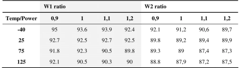
Table 3. FWi/Fmax ratio for a typical process corner
W1 ratio W2 ratio Temp/Power 0,9 1 1,1 1,2 0,9 1 1,1 1,2 -40 95 93.6 93.9 92.4 92.1 91,2 90,6 89,7 25 92.7 92.5 92.7 92.5 89.8 89,2 89,4 89,9 75 91.8 92.3 90.5 89.8 89.3 89 87,4 87,3 125 92.1 90.5 90.3 90 88.8 87,9 87,2 87,5
Behavior validation and performances. In order to check if the whole system remains functional, we extracted from simulation (a) the maximum operating frequency Fmax of the circuit at different PVT conditions (b) the maximum frequencies FW1 and FW2 at which the monitoring system does not flag any timing warnings or violations, con-sidering respectively two different detection windows W1 and W2; W2 corresponding to the largest detection window. Table 2 gives the simulated results for FW1/Fmax and FW2/Fmax ratios at different VT conditions for a nominal process (other process corners demonstrate similar efficiency):
• FW1/Fmax and FW2/Fmax ratios remain lower than 100% meaning that the monitoring system operates correctly and warns an imminent timing failure, in every PVT conditions.
• Considering the global PVT conditions, the timing margins Tm(W1) and Tm(W2) remain respectively between 80/340 and 120/480 ps when the sys-tem operates correctly.
These results demonstrate the efficiency of the monitoring system in making it par-ticularly interesting for adaptation: the circuit can work at roughly 90% of its maximal speed under all PVT conditions and the system is very attractive in nominal and best cases to crop margins or decrease consumption. It can also be favorable to integrate two different detection windows to control the timing margins with accuracy during the voltage scaling.
5 Conclusion
This paper describes a new in situ monitoring system, based on the insertion of sen-sors close to observable flip-flop endpoints, coupled with specific clock tree cells providing detection windows. This system prevents from timing violations rather than detecting an error. Valuable and simulated in a wide range of environmental condi-tions, this timing slack monitoring system, compact and with little impact on the over-all power consumption, can thus be used together with knob-based adaptive solutions. A dedicated flow based on a standard design flow was described, easing the inser-tion of the specific detecinser-tion material and allowing a clear critical path endpoint choice to reduce the number of paths to be monitored. Simulation results demonstrate the efficiency of such a system and its easy integration, making it very attractive to work at the optimal PVT operating point for critical IP blocks in advanced technologies.
References
1. Narayanan, V., et al.: Proc. 18th ACM Great Lakes Symposium on VLSI, Orlando, Flor-ida, USA (2008)
2. Lasbouygues, B., et al.: Temperature- and Voltage-Aware Timing Analysis. IEEE Trans. on CAD of Integrated Circuits and Systems 26(4), 801–815 (2007)
3. Parthasarathy, C., Bravaix, A., Guérin, C., Denais, M., Huard, V.: Design-In Reliability for 90-65nm CMOS Nodes Submitted to Hot-Carriers and NBTI Degradation. In: Azé-mard, N., Svensson, L. (eds.) PATMOS 2007. LNCS, vol. 4644, pp. 191–200. Springer, Heidelberg (2007)
4. Nourani, M., Radhakrishnan, A.: Testing On-Die Process Variation in Nanometer VLSI. IEEE Design & Test of Computers 23(6), 438–451 (2006)
5. Samaan, S.B.: Parameter Variation Probing Technique: US Patent 6535013 (2003) 6. Persun, M.: Method and apparatus for measuring relative, within-die leakage current
and/or providing a temperature variation profile using a leakage inverter and ring oscilla-tors: US Patent 7193427 (2007)
7. Drake, A., et al.: A Distributed Critical Path Timing Monitor for A 65nm High Perform-ance Microprocessor. In: ISSCC, pp. 398–399 (2007)
8. Das, S., et al.: A Self-Tuning DVS Processor Using Delay-Error Detection and Correction. IEEE JSSC 41(4), 792–804 (2006)
9. Blaauw, D., et al.: Razor II: In situ error detection and correction for PVT and SER toler-ance. In: ISSCC, pp. 400–401 (2008)
10. Bowman, K.A., et al.: Energy-Efficient and Metastability-Immune Timing-Error Detection and Instruction-Replay-Based Recovery Circuits for Dynamic-Variation Tolerance. In: ISSCC, pp. 402–623 (2008)
11. Rebaud, B., et al.: An Innovative Timing Slack Monitor for Variation Tolerant Circuits. In: ICICDT (2009)
12. Agarwal, M., et al.: Circuit Failure Prediction and Its Application to Transistor Aging. In: Proc. VLSI Test Symposium, pp. 277–286 (2007)
13. Migairou, V., Wilson, R., Engels, S., Wu, Z., Azemard, N., Maurine, P.: A Simple Statisti-cal Timing Analysis Flow and Its Application to Timing Margin Evaluation. In: Azémard, N., Svensson, L. (eds.) PATMOS 2007. LNCS, vol. 4644, pp. 138–147. Springer, Heidel-berg (2007)
14. Blaauw, D., et al.: Statistical timing analysis: From basic principles to state of the art. IEEE Trans. on CAD of Integrated Circuits and Systems 27(4), 589–607 (2008)