HAL Id: tel-00870365
https://tel.archives-ouvertes.fr/tel-00870365
Submitted on 7 Oct 2013HAL is a multi-disciplinary open access archive for the deposit and dissemination of sci-entific research documents, whether they are pub-lished or not. The documents may come from teaching and research institutions in France or abroad, or from public or private research centers.
L’archive ouverte pluridisciplinaire HAL, est destinée au dépôt et à la diffusion de documents scientifiques de niveau recherche, publiés ou non, émanant des établissements d’enseignement et de recherche français ou étrangers, des laboratoires publics ou privés.
Boîtes quantiques de semi-conducteurs nitrures pour des
applications aux capteurs opto-chimiques
Aparna Das
To cite this version:
Aparna Das. Boîtes quantiques de semi-conducteurs nitrures pour des applications aux capteurs opto-chimiques. Autre [cond-mat.other]. Université de Grenoble, 2012. Français. �NNT : 2012GRENY028�. �tel-00870365�
THÈSE
Pour obtenir le grade de
DOCTEUR DE L’UNIVERSITÉ DE GRENOBLE
Spécialité : Physique / Nanophysique
Arrêté ministériel : 7 août 2006
Présentée par
Aparna DAS
Thèse dirigée par Eva MONROY
préparée au sein du Laboratoire Nanophysique et Semi-Conducteurs
(CEA / INAC / SP2M)
dans l'École Doctorale de Physique
Boîtes quantiques de
semi-conducteurs nitrures pour
des applications aux capteurs
opto-chimiques
Thèse soutenue publiquement le 13 juin 2012 devant le jury composé de :
Mme Chantal FONTAINE
Rapporteur M Nikos T. PELEKANOS Rapporteur M Henri MARIETTE Président M Bernard GIL Membre
Mme Philomela KOMNINOU
Membre
Mme Eva MONROY
Membre
Acknowledgement
My thesis work would not have been possible without the guidance and the help of various people who in one way or another contributed and extended their valuable assistance in the preparation and completion of this study. It is a pleasant task to express my thanks to all those who contributed to the success of this study.
First and foremost, my utmost gratitude to my thesis advisor Dr. Eva Monroy, without her guidance, support and encouragement this work would not have been possible. She taught me everything, from A to Z, and I strongly believe that, I am one of the luckiest PhD students in the word to have a thesis advisor like her. Her prodigious knowledge, promptness to everything, composed nature made me to grow more and my work interesting, my deepest gratitude to my mentor.
My sincere thanks go to Prof. Henri Mariette, Director of the group Nanophysics and semiconductors Prof. Jean-Michel Gerard, Director of the division on physics of materials and microstructures of INAC, for their able leadership has created a positive and learning environment for all the members of the lab. Special thanks to Prof. Henri Mariette for being the president of jury.
I convey my thanks to the members of the jury: Referees Dr. Chantal Fontaine (LAAS-CNRS), and Prof. Nikos T. Pelekanos (University of Crete, Greece), Examinators Prof. Bernard Gil (CNRS, Montpellier), Prof. Philomela Komninou (Aristotle University of Thessaloniki, Greece), Ass. Prof. Fernando B. Naranjo (Universidad de Alcalá, Spain) for accepting to serve in the jury, despite of their busy schedule.
Concerning the external collaborations, I would like to thank Prof. Ph. Komninou and her group at Aristotle University of Thessaloniki, for helping me for microscopic analysis of my samples and providing us high quality TEM data. I also would like to thank Dr. K. Lorenz at Instituto Tecnológico e Nuclear, Portugal for the RBS measurements. I take this opportunity to thank Prof. M. Eickhoff and his group at Justus-Liebig-Universität Giessen, Germany and Dr. A. Helwig and his group at EADS,
Germany for chemical analysis and for design of our sensor system. I am grateful to Prof. Pierre Ruterana (ENSICAEN-CNRS) and Dr. Eirini Sarigiannidou (INPG) for their support in microscopic analysis. Thanks are due to G. Nataf and Ph. De Mierry from CHREA-CNRS for providing semipolar GaN templates, and to DOWA for polar AlN templates.
Many thanks to Joel Bleuse and Bruno Gayral for helping me with the optical characterization of samples. I would also acknowledge Edith Bellet-Almaric for her support in diffraction experiments. My special thanks go to the technicians of our lab Yoann Cure, Yann Genuist and Jean Dussaud for supporting us with their MBE expertise regularly. Special acknowledgements to Carmelo and Cécile, for their indispensable help related with administrative work.
I would like to acknowledge Lise and Prem for their support to learn about MBE machine. I am deeply indebted to Yulia for her support and entertainment. Yulia, thanks for sharing the office with me and scolding me when I came late in the office. Very special thanks to Fernando and Sirona for their comments and encouragement during rehearsal. Sirona, thanks for the Spanish sweet, my parents will really love that. Fernando, I learned a lot from you and thanks for helping me with the origin graphs and mental support during my defense.
Words are short to express my deep sense of gratitude towards my friends, Kannan, Nitin, Sandeep, Rajeev, Siddharth, Veeresh, Anna, Karine, Diane for their support.
I am gratefully acknowledges the financial support from the EU FP7 project DOTSENSE (STREP 224212) and the French National Research Agency project COSNI (BLAN08-1_323691).
Lastly, and most importantly, I wish to thank my family and the special person who made all this possible.
Résumé
Ce travail de thèse a porté sur la synthèse de boîtes quantiques (BQs) de semi-conducteurs nitrures orientés (11-22) ou (0001) par épitaxie par jets moléculaires à plasma d’azote, pour des applications aux capteurs chimiques pour la détection du niveau de pH, d’hydrogène ou des hydrocarbures dans des environnements gazeux ou liquides.
Les trois premiers chapitres sont généraux. Le premier chapitre présente l’état du domaine et précise les objectifs de la thèse. En particulière il y est expliqué comment une polarisation piézoélectrique et spontanée est présente dans les couches nitrures du fait de leur structure wurtzite. Pour empêcher cette propriété très gênante pour les applications optoélectroniques, une proposition consiste à changer l’orientation cristalline des couches. Dans le cadre de cette thèse, la possibilité d'utiliser la croissance de structures dans des directions semipolaires (de polarité faiblement marquée) a été visée, ces dernières pouvant assurer un bon compromis si la qualité structurale des matériaux est meilleure que celle obtenue pour les matériaux d'orientation non polaire, contenant une grande densité de défauts. Enfin, il a été choisi d'exploiter les structures à boîtes quantiques GaInN car elles devraient minimiser l'effet des recombinaisons non-radiatives, qui s'avèrent très néfastes pour les puits quantiques. Aussi dans ce premier chapitre, j’explique le cadre applicatif de mon travail. Le domaine des capteurs, qui est en pleine explosion, a jusqu'ici reposé sur la technologie silicium. Or les nitrures possèdent des propriétés qui correspondent au cahier des charges de ces applications et aussi à certains de leurs besoins, en particulier pour les capteurs chimiques.
Le second chapitre précise les propriétés des nitrures du groupe III. Ce chapitre rappelle tout d'abord les différentes formes cristallines que peuvent prendre ces semiconducteurs, notamment la forme wurtzite qui est la plus stable, et explicite le problème de polarité, qui conduit à la présence du champ piézoélectrique interne spontané, et sa relation à l'orientation cristalline. Je commente ensuite la structure de bande de ces matériaux et leur dépendance à la température, ainsi que les valeurs de masse effectives publiées pour les électrons et les trous. Les propriétés élastiques sont
matériaux contraints pour les orientations polaire (0001) et semi-polaire (11-22). Les polarisations engendrées par les piézoélectricités spontanée et induite par les déformations sont enfin précisées et leur effet sur la structure de bande des puits quantiques rappelée.
Le troisième chapitre décrit les techniques expérimentales sollicitées dans ces travaux. Je discute d'abord de la technique d'épitaxie qu'elle a utilisée, la technique d'épitaxie par jets moléculaires (MBE). Après en avoir rappelé brièvement les principes généraux, le bâti utilisé est décrit. Le principe de la technique de diffraction électronique en incidence rasante (RHEED) est ensuite présentée, ainsi que les informations qui peuvent en être tirées sur l'évolution du paramètre de maille du matériau en croissance, l'arrangement atomique de sa surface et la vitesse de croissance. Le choix du substrat de saphir est alors précisé, ainsi que les relations d'épitaxie entre le GaN et le saphir, de structure rhomboédrique, qui dépendent bien sûr de son orientation. Les défauts ponctuels et les dislocations qui sont présents dans les couches sont discutés. Le chapitre se termine par une présentation des techniques de caractérisation, diffraction de rayons X, microscopie à force atomique et spectroscopie de luminescence, mises en jeu dans ces travaux. A la fin de ce chapitre, les informations nécessaires à la compréhension de l'étude menée sur l'élaboration des multicouches à puits et boîtes quantiques et leur caractérisation ont été données.
Les trois derniers chapitres concernent ma contribution personnelle. L'épitaxie par jets moléculaires de couches (11-22) semipolaires est traitée dans le quatrième chapitre successivement pour les matériaux AlN, GaN , GaInN et InN. Dans les deux premiers cas, le but était de mieux comprendre l'origine des défauts rencontrés dans les travaux précédents de l'équipe. Ainsi, pour AlN, il s'est agi de préciser l'origine du polycristal formé pendant la croissance, constitué de grains orientés (11-22) et (10-10), dont la densité tend à diminuer quand le rapport III/V diminue. Mon étude a montré que ces grains se forment dès les premiers stades de la germination d'AlN dans le cadre d'une collaboration avec l'Université de Thessalonique, par une étude couplée de microscopie en transmission (MET), RHEED et AFM. L'existence de ces zones parasites a été reliée à la présence de nanofacettes localement formées à la surface du saphir, par réaction avec l'AlN, en particulier lors du départ de l'épitaxie sous flux d'azote. L'optimisation de ce matériau est importante car il va être utilisé comme
tampon pour le GaN. En effet, dans le cas du GaN (11-22), l'épitaxie directe sur saphir conduit à la présence de deux orientations, mais l'utilisation d'un tampon AlN permet d'obtenir uniquement l'orientation visée. J’ai trouvé que l'optimisation du matériau orienté (11-22) consistait à contrôler le léger excès de gallium imposé pendant l'épitaxie car il conduisait plus rapidement à l'accumulation de Ga que pour l'orientation (0001).
Je me suis ensuite intéressée à la réalisation de couches dopées de GaN dopées. Des couches épaisses de GaN:Mg ont pu être réalisées avec des dopages élevés (1,6 × 1020 cm-3), sans y observer les défauts identifiés pour l'orientation (0001) par microscopie ou sur les spectres de photoluminescence. Le dopage N du GaN (11-22) par le silicium a pu être réalisé sans ennui, les conditions trouvées étant les mêmes que celles de couches non dopées.
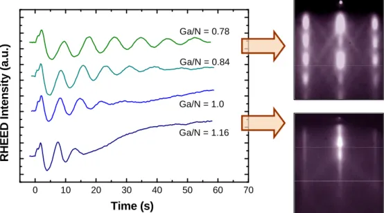
De la même façon, l'épitaxie de couches d'AlGaN de bonne qualité peut être réalisée, mais en utilisant un rapport III/V plus faible que pour (0001). Le problème est plus complexe pour le ternaire GaInN. Aussi, j’ai étudié la désorption d'indium d'une surface GaN (11-22) en la comparant au cas de référence (0001). J’ai pour cela exploité les variations temporelles d'intensité du RHEED. J’ai utilisé ces données pour étalonner la température de croissance, puis pour préciser la quantité d'excès d'indium optimal, qu'elle a à nouveau trouvé égal à 2 monocouches pour cette surface (même si l'arrangement atomique de ces deux surfaces diffèrent). Les couches épaisses réalisées sous ces conditions conduisent cependant à des surfaces facettées. La présence de dislocations dans les couches a été identifiée par MET comme origine de ces facettes. Un autre résultat important identifié est que l'incorporation de l'indium y est cinq fois plus faible que pour (0001). Ce résultat, en contradiction avec la théorie et les matériaux MOVPE, est bien confirmé par les spectres de luminescence de ces couches.
La fin de ce chapitre est consacrée à l'étude menée par A. DAS sur l'épitaxie d'InN orienté (0001) et (11-22). Cette croissance est difficile car elle doit être réalisée dans certains cas à température beaucoup plus faible (450°C au lieu de 600-700°C pour InGaN), pour laquelle la désorption de l'InN est plus rapide que celle de l'indium. Pour l'orientation (0001), cette propriété a été exploitée pour connaitre le rapport
conjointement. Les propriétés de luminescence de ces matériaux indiquent des déviations par rapport aux prévisions, en particulier pour l'InN (11-22) dont l'émission ne suit pas la loi en température de Varshni, alors que la recombinaison non radiative y est toutefois moins forte que pour l'orientation (0001).
Le cinquième chapitre porte sur la réalisation de structures à plans empilés de boîtes quantiques (In)GaN/AlN (QDs). Je rappelle d'abord les résultats obtenus sur les QDS de GaN/AlN (0001). Je précise les techniques utilisables pour leur obtention, croissance en condition riche N, ou en condition Ga avec arrêt, avec une moins grande densité dans le second cas, qui sera la technique qu'elle utilisera. Je rappelle finalement l'intérêt de ces nanostructures qui conduisent à une grande stabilité en luminescence en température, avec une efficacité interne quantique beaucoup plus élevée, mais à des spectres plus larges que pour les multi-puits quantiques (MQW) du même type.
La forme des QDs GaN/AlN (11-22) obtenus en condition riche Ga avec arrêt de croissance a été identifiée par MET à Thessalonique, et présente deux variantes: rectangle ou trapèze. Les propriétés de luminescence des QDs sont celles attendues pour ces nanostructures, mais comparées au cas (0001), on remarque que la réduction du champ piézoélectrique modifie leur gamme d'émission, d'énergie plus resserrée mais plus élevée que le gap du GaN, et diminue d'un ordre de grandeur le temps de déclin de luminescence. Dans le cas des QDs InGaN/AlN, pour (0001), des MQW et QDs ont été réalisés. La MET met en évidence une certaine interdiffusion aux interfaces supérieures des MQW et l'absence de défauts d'empilement dans les QDs. La spectroscopie de luminescence indique que la température de croissance conduit à une diminution de la longueur d'onde d'émission, reliée logiquement à une augmentation en In dans les MQW, alors que la tendance est moins nette pour les boites quantiques. J’explique ce résultat en considérant que dans ce cas, la forme des QD évolue avec la concentration en In. Quand l'indium est augmenté, non seulement l'énergie de leur émission de luminescence diminue mais la largeur à mi-hauteur augmente, certainement du fait de leur plus grande dispersion. De plus, les effets de localisation de porteurs dus à des fluctuations de potentiel observés quand on augmente la température deviennent plus prononcés. Pour les QW, la dépendance en température indiquent des fluctuations de contenu en indium. Il serait logique que les
fluctuations rencontrées dans les QDs soient du même type. La situation s'avère plus complexe pour les QD orientées selon (11-22). Dans un premier temps, une température qui permet la désorption de l'indium est utilisée, mais les observations MET indiquent que les boîtes s'épitaxient en partie sur des plans inclinés, du fait de la contrainte qui courbe la surface, et éventuellement à la présence de défauts d'empilement, à la proximité desquels elles se forment apparemment préférentiellement. Ceci peut effectivement s'expliquer par le fait que la formation de ces défauts linéaires, qui précèdent celle des QD, peut aussi être due aux contraintes, d'autant plus qu'une composante de cisaillement est autorisée pour cette orientation, et que ces défauts contiennent des dislocations à leur extrémité. Cela pourrait permettre une relaxation des contraintes au sein des boîtes. Réalisée à basse température où la désorption d'indium est négligeable, l'épitaxie de QDs conduit à la présence à une forte distorsion de la surface par une grande densité de ST multiples. Elles restent toutefois bien identifiables sur la coupe transversale de MET alors que ce n'est pas le cas pour les QDs (0001), qui contiennent une densité très forte de SFM. La comparaison de la photoluminescence des structures réalisées à différentes températures est menée. Alors que pour les températures plus élevées (650-690°C), l'énergie d'émission des boites indique que l'incorporation d'indium est beaucoup faible même pour les QDs (0001) faible, ce d'autant plus que la température est élevée, cette énergie diminue drastiquement pour les basses températures d'épitaxie. Le confinement 3D est confirmé en comparant leur évolution en température avec celles de QW. Pour les QDS épitaxiées à haute température, les recombinaisons non radiatives y sont plus présentes que pour l'orientation polaire, alors qu'elles diminuent quand la longueur d'onde d'émission des QD augmente (plus faible température d'élaboration). Il n'y a plus de luminescence des QDS (0001), sinon une émission constante, qui serait due à la présence de poches cubiques liées aux SFM. Ce chapitre se conclut sur les mesures de contraintes par MET menées à Thessalonique. Les tendances données par ces résultats confirment les observations précédentes.
Enfin, le sixième chapitre présente les résultats obtenus par nos partenaires de contrat sur les composants que j’ai a réalisés. Des capteurs à base de QDS et MQW GaN/AlN ont été épitaxiés et processés. Les caractéristiques de photoluminescence sous polarisation électrique indiquent une bonne sensibilité. Toutefois, un courant
tunnel parasite participe à la génération de porteurs si les barrières AlN des QD sont trop fines. La réponse du capteur à la présence d'hydrogène est très contrastée. Le signal est toutefois saturé dès que l'hydrogène excède 10% de concentration sans courant tunnel, et 500 ppm en présence de courant tunnel. La conclusion tirée est que seuls les plans de QD supérieurs sont affectés par l'hydrogène et effectivement le contraste du composant est meilleur pour un composant à un seul plan de QD. Ces résultats ont été obtenus pour les QDs (0001).
En effet, l'utilisation des QDs (11-22) a conduit à des émissions de luminescence d'énergie supérieure au gap, donc non utilisables, d'où la nécessité d'ajouter de l'indium à ces QDs. Des composants à base de GaInN/GaN (0001) et (11-22) ont alors été réalisés. Seules les structures (0001) ont donné des émissions de photoluminescence à température ambiante. Les premières demandent encore une optimisation plus poussée pour réaliser les composants entiers qui comprennent des empilements complexes des différents nitrures. Les composants à QDs (0001) se sont en revanche révélés excellents, leur réponse à la tension externe étant extrêmement sensible. Ainsi, des capteurs ont permis de mesurer le pH de l'eau de 0 à 7 d'une manière très efficace. A la suite de cette validation, j’ai conclu mes travaux en dressant un cahier des charges pour la réalisation de ces composants.
Contents
1 Introduction and targets
1
1.1 Historical introduction of III-nitride semiconductors 1 1.2 Wide bandgap semiconductors for chemical sensors 5
1.3
Motivation and targets 6
1.4 Organization of the manuscript 9
Bibliography 11
2 Properties of III-nitride semiconductors
15
2.1 Crystalline structure 15
2.1.1
Crystal symmetry and lattice parameters 15
2.1.2 Crystal polarity 19
2.2 Electronic properties 20
2.2.1 Band structure 20
2.2.2 Temperature dependence of the fundamental band gap 22
2.2.3
Effective masses 23
2.3 Elastic properties 24
2.3.1 Strain and stress 24
2.3.2 Biaxial stress in a (0001)-oriented hexagonal system 26 2.3.3 Strain in semipolar layers under biaxial stress 26 2.4 Spontaneous polarization and piezoelectricity 29 2.4.1 Polarization effects in heterostructures 30
Bibliography 32
3
Experimental techniques
37
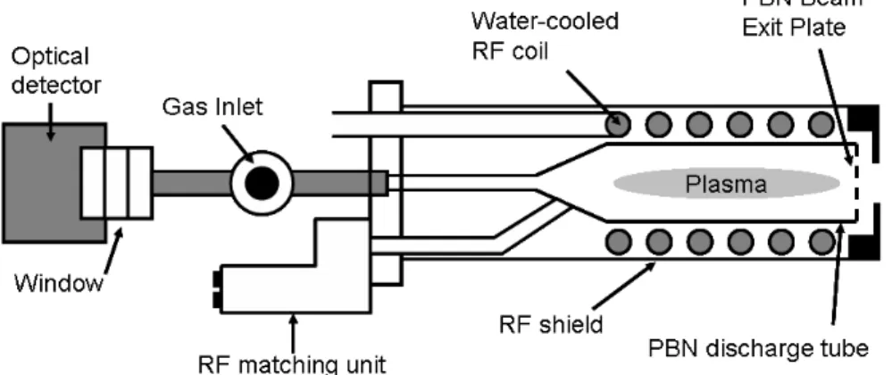
3.1 Epitaxial growth 37
3.2
Plasma-assisted molecular beam epitaxy 39 3.3 Reflection high-energy electron diffraction (RHEED) 42
3.4 PAMBE of III-nitrides 44
3.4.1 Growth of GaN (0001) 45
3.4.2 Growth of AlN (0001) 48
3.4.3 Growth of polar (0001) AlGaN 48
3.4.4 Growth of polar (0001) InGaN 49
3.5 Substrates 49
3.5.1 Sapphire-based substrates 50
3.6 Defects observed in III-nitrides 52
3.6.2 Line defects 53
3.6.3 Planar defects 56
3.7 Characterization methods 57
3.7.1 X-ray diffraction 57
3.7.2 Atomic-force microscopy (AFM) 60
3.7.3 Photoluminescence spectroscopy 65
Bibliography 67
4 Plasma-assisted MBE of semipolar (11-22)-oriented 2D layers
Experimental techniques
71
4.1 Introduction 71
4.2 Semipolar (11-22) AlN 71
4.2.1 Growth of single-phase (11-22) AlN 71 4.2.2 AlN nucleation on m-sapphire substrate 74
4.3 Semipolar (11-22) GaN 79
4.3.1 PAMBE growth kinetics of GaN(11-22) 79
4.3.2 p-type doping of GaN(11-22) 81
4.3.3 n-type doping of GaN(11-22) 84
4.4 Semipolar (11-22) AlGaN 85
4.5 Semipolar (11-22) InGaN 87
4.5.1 Temperature calibration 87
4.5.2 In kinetics on semipolar GaN 89
4.5.3 Growth details and properties of semipolar InGaN layers 92
4.6 Semipolar (11-22) InN 99
4.7 Conclusions 107
Bibliography 110
5
Polar and semipolar (In)GaN QDs
113
5.1 III-Nitride quantum dots 113
5.2 Polar GaN/AlN quantum dots 114
5.3 GaN/AlN QDs with reduced internal electric fields 121
5.4 Polar InGaN/GaN QDs 126
5.5 InGaN/GaN QDs with reduced internal electric field 133 5.6 Growth of semipolar InGaN QDs at low- TS 139
5.7 Lattice strain and indium content in the InGaN QDs 144
5.8 Conclusions 146
6 Opto-chemical sensors based on (In)GaN QDs as optical
transducers
153
6.1 Introduction 153 6.2 Description of the opto-chemical transducers 154
6.3 Polar GaN/AlN QDs opto-chemical transducers 155 6.3.1 Synthesis and characterization 155
6.3.2 Emission characteristics of GaN QDs in external electric fields 159 6.3.3 Hydrogen sensitivity of GaN QDs transducers 162
6.4 Semipolar GaN QD opto-chemical transducers 163 6.5 Polar InGaN QD opto-chemical transducers 165 6.5.1 Synthesis and characterization 165
6.5.2 Emission characteristics of InGaN QDs in external electric fields 168 6.5.3 pH-sensitivity of InGaN QDs transducers 171 6.6 Semipolar InGaN QD opto-chemical transducers 172 6.6.1 Synthesis and characterization 172
6.6.2 Emission characteristics of semipolar InGaN QDs in external electric fields 174 6.7 Chemical sensor system based on InGaN QDs 174
6.8 Conclusions 177 Bibliography 180
7
Conclusions and perspectives
181
Annex
187
Glossary
191
Chapter 1
Introduction and targets
1.1 Historical introduction of III-nitride
semiconductors
Group III-nitride semiconductors (GaN, AlN and InN) are currently the materials of choice for ultraviolet/blue/green light emitters and high power electronics. The electronic band structure for each of the nitride materials possesses a direct transition with a band gap energy ranging from 0.64 eV ([Wu09] and references therein) for InN to 3.4 eV for GaN, and to 6.2 eV for AlN, as illustrated in Figure 1.1. Thus, these semiconductors and its alloys could cover most of the solar spectrum range. Besides this, characteristics such as high mobility, high breakdown voltage, high electron saturation velocity, high thermal conductivity, chemical inertness, and mechanical stability make them well suited for designing and fabricating high-power, high-frequency and high-temperature electronic devices [Dec08, Pea99].
The first studies of the growth of polycrystalline III-nitrides go back to 1907, when Fichter et al. [Fic07] reported the synthesis of AlN when aluminum is burned in the air or heated in nitrogen to a high temperature. Following that, Johnson et al. [Joh32] reported the synthesis of GaN in 1932, and Juza and Hahn [Juz38] demonstrated the growth of InN. The first important breakthrough in the research history of group III nitrides occurred when a number of workers began applying hetero-epitaxial growth on sapphire substrates to produce GaN films with reasonable crystalline quality, in 1969 by hydride vapor phase epitaxy (HVPE) [Mar69], in 1971 by metal-organic vapor phase epitaxy (MOVPE) [Man71] and in 1975 by molecular beam epitaxy (MBE) [Yos75].
All the GaN made at that time was very conducting n-type even when not deliberately doped. The lack of p-type conductivity coupled with somewhat poor crystalline quality blocked the development of nitride-based devices for several years. Another major breakthrough was the first successful production of p-type GaN using Mg, in 1989, by Amano et al., [Ama89], which later resulted in the first fabrication of highly efficient blue light emitting diodes (LEDs) (1994) and laser diodes (LDs) (1996) by Nakamura et al. [Nak94, Nak96]. Since 1994, the research activities on these materials increased rapidly because of their commercial applications.
Several techniques are currently used for the epitaxial growth of III-V nitride semiconductors. Among these techniques, MBE and MOCVD (Metal-organic chemical vapor deposition) are the most popular, due to their capability to produce films and heterostructures with the crystalline quality required for short-wavelength optoelectronic devices, and high-power high-frequency electronic devices. In the early years, MBE growth had faced some difficulties to prepare nitride epilayers, due to the lack of a proper nitrogen source, and at that time it has been surpassed by MOCVD. Thanks to the developments in the nitrogen plasma sources, MBE grown materials can now compete well with MOCVD in terms of material quality, but not in terms of surface and production throughput. Nevertheless, MBE keep several advantages over MOVPE for nanostructure fabrication. For example, the low growth temperature makes it possible to achieve chemically sharper interfaces, it is particularly adequate for the growth of InN and high-In content alloys, it offset a wide flexibility for the growth of three-dimensional (3D) nanostructures like quantum dots
(QDs) and nanowires (NWs), no post-growth activation of Mg dopants is required and Mg memory effects are reduced, which leads to sharper Mg doping profiles.
Many of the major problems that have hindered the progress in III-nitride related semiconductors can be traced back to the lack of native substrates for epitaxial growth. Most of the III-nitride-based devices are grown on foreign substrates such as sapphire or silicon carbide. Due to the destitution of the substrate with similar lattice parameters and thermal expansion coefficients, the III-nitride epitaxial layers usually contain numerous crystalline defects. The defect densities in nitride epilayers (107 -1010 cm-2) are much higher than those of other III-Vsemiconductors (e.g., for arsenide or phosphide materials, 102-104 cm-2). In addition, the mismatch of thermal expansion coefficients induces thermal stress in the film and substrate during cooling down to room temperature, which can lead to bowing and even cracking of the epitaxial films. It is expected that the performance of the nitride devices will be improved with native substrates, in part due to the elimination of lattice and thermal expansion mismatch between the device layers and the substrate. Nowadays the researchers are using conductive free-standing GaN substrates created via HVPE [Kel99], since the growth of bulk GaN crystals is a challenge due to their high melting temperature, very high equilibrium nitrogen vapor pressure at moderate temperatures, and low solubility in acids, bases and most other inorganic elements and compounds. However, free-standing GaN substrates are much more expensive than the sapphire substrates used commercially as a base for nitride growth.
Another main problem with nitride semiconductors is related to the polar nature of the material. Because of their crystalline structure, III-nitride semiconductors exhibit strong spontaneous and piezoelectric polarization along their growth axis, the c-axis [Ber97], which leads to strong internal fields of the order of some MV/cm in quantum wells (QWs) and heterostructures [Mar96, Ler98]. Even though this large internal electric field has potential applications in piezoelectric sensors and high electron mobility transistors (HEMT) [Gas97], it has deleterious effect on the performance of optoelectronic devices, where they lead to the quantum confined Stark effect (QCSE) and reduce the radiative recombination rate within the heterostructures.
Figure 1.2: Piezoelectric polarization of an InxGa1–xN quantum well as a function of the
growth direction.
In order to overcome these polarization-related problems, nitride heterostructures need to be grown along crystallographic directions where the internal electric field is small or zero, that is, on semipolar planes (tilted in the range of 0° to 90° with respect to c-plane) or on nonpolar planes (tilted 90° with respect to c-plane). Figure 1.2 shows the piezoelectric polarization of an InxGa1–xN QW grown
pseudomorphically between relaxed GaN barriers [Par99]. Here P′z is the polarization
perpendicular to the growth plane and the lattice planes of particular polar, semipolar, and nonpolar orientations are shown as insets.
Around the year 2000 the research field of non-polar III-nitrides started to emerge in an effort to eliminate the QCSE in the heterostructures and thus achieve higher internal quantum efficiency. Waltereit et al. first demonstrated the absence of the piezoelectric field in m-plane GaN/AlGaN QWs grown on LiAlO2 substrates [Wal00]. A reduction of the electric field has also been observed in QDs grown in nonpolar orientations [Fou05, Ams07]. However, nonpolar nitride growth remains challenging due to the strong anisotropy of their surface properties, which leads to epitaxial layers with a high density of crystalline defects.
Another approach is the growth of the heterostructures in semipolar directions. Semipolar crystallographic orientation in the growth direction can have the potential
to reduce the polarization-induced internal electric field in the nitride structures and are subject of intense investigation in the last three years as preferred growth orientation for green/yellow light emitting diodes and lasers. Benefits like reduction in piezoelectric field strength has been experimentally verified for nitride heterostructures grown along (10-1-1), (10-1-3), and (11-22) semipolar directions [Cha05, Nis04]. Furthermore, epitaxial growth along semipolar directions appears easier to control, semipolar-grown films also incorporate indium — a crucial element in the LED — more efficiently, and have a wider growth window than nonpolar films. However, growth on alternative crystallographic orientations, like semipolar orientations, implies new defect structures, due to the enhanced probability of stacking fault formation and availability of gliding planes [Tya09], which results in an enhancement of the nonradiative recombination rate.
An advantage of QDs is that excitons trapped in these objects are expected to be much more insensitive to nonradiative recombination than other semiconductor structures, such as QWs, due to the 3D electronic confinement [Ger96]. Thus, QDs in these semipolar orientation are believed to be capable of avoiding the carrier migration to nonradiative recombination centers, and thereby the possibility of enhanced internal quantum efficiency.
1.2 Wide bandgap semiconductors for chemical
sensors
Key innovations in the field of chemically-sensitive field-effect structures are due to the pioneering work of Lundström [Lun75], Bergveld [Ber70] and their coworkers. These researchers demonstrated in the nineteen-seventies that hydrogen-sensitive field-effect devices and ion-hydrogen-sensitive field-effect transistors could be formed using silicon-based semiconductor technology. Research along these lines remained a subject of intense interest up to the present days. Whereas in the first two decades, various kinds of gas- and ion-sensitive metal-oxide-semiconductor (MOS) capacitors and field-effect transistors were realized using the standard silicon-technology, the range of applications of chemically-sensitive field-effect devices was significantly
extended by two follow-on innovations: the first was applying SiC as a substrate material for enabling high-temperature applications, such as exhaust gas sensors required for novel kinds of exhaust gas after-treatment [Llo97]. The second innovation relates to the scanning light-pulse technique (SLPT), which allows for a spatially resolved detection of chemically induced variations in the surface potential [Lun91], and which has recently enabled developments such as computer screen-assisted remote diagnostics [Fil05]. In SLPT, the achievable spatial resolution is limited by the minority carrier diffusion length. As far as bioelectronic applications in liquid environments are concerned, the development has culminated in highly-integrated, Si-based solution-gate field-effect transistor arrays for the spatially-resolved electronic detection of neuron activity and neural signal transmission [Eve03].
More recently, other wide-bandgap semiconductors, such as diamond or the group III-nitride system, have been shown to bear promising material properties for the application in chemical and biochemical sensors. Besides their capability of high-temperature operation, which allows the realization of high-high-temperature gas sensors as for instance Pt:GaN Schottky diodes [Lut99, Sch02] or AlGaN/GaN field effect transistors [Sch02b], the high electrochemical surface stability of these compound semiconductors also enables novel biochemical sensor applications in liquid electrolytes [Ste03, Bau06]. Using such materials, a largely improved stability is attained with regard to conventional silicon devices.
1.3 Motivation and targets
Besides their unique optoelectronic properties, III-nitride semiconductors also exhibit material characteristics favorable for the realization of chemical sensors: high chemical and thermal stability [Eic03], and a high pH-sensitivity in liquid solutions [Ste03]. Furthermore, this material system and sapphire as the respective substrate material offer the unique advantage of being transparent to visible light, which enables transducer integration into setups for opto-chemical analyses (e.g. fluorescence spectroscopy [Ste03b]).
These concepts were the motivation of the 7th European Framework Project DOTSENSE (STREP 224212) which ran between 2008 and 2011 and set the basis of this PhD work. In this project we proposed to combine the optical properties of III-nitrides (transparency, direct bandgap, efficient luminescence) with their chemical surface properties in order to develop novel kinds of opto-chemical sensor systems. There, chemically-induced variations in the surface potential are detected by induced changes in the luminescence of III-nitride nanostructures, namely (In)GaN self-assembled QDs (Figure 1.3). This detector design allows exploiting the capability of III-nitride materials for operation under harsh environment conditions (high pressure, explosive media), as neither electrical feedthroughs nor a deterministic current are necessary for the sensor signal read-out. Furthermore, the progress in nitride technology opens up the possibility to integrate these transducers with commercially-available light emitters and detectors to form novel integrated opto-chemical sensor system architectures.
The requirement on the transducers of providing intense room-temperature photoluminescence (PL) is satisfied by the introduction of QD structures as optically active media. As described above, the 3D confinement in these nanostructures suppresses thermally activated non-radiative recombination processes. The development of III-nitride technology allows achieving QD ensembles emitting in a range of wavelengths extending from the UV to the green region. Within this range, efficient room-temperature PL can be observed, even in the case of a single QD layer. To take advantage of commercial III-nitride emitters and detectors, the sensor system should operate in the blue-green spectral range. Finally, we decided to assess the growth of QDs on non-polar or semipolar orientations in order to enhance the sensitivity of the transducers.
Figure 1.3: Group III-nitride QD test structures. The Si-doped AlGaN layer serves as a back contact for applying a defined potential difference across the QD stack. A bare (oxidized) surface is used in case of pH detection in liquids, a catalytic Pt-top contact is used for hydrogen detection.
Therefore, my thesis work has focused on the PAMBE growth of (In)GaN-based QD structures, grown in both polar and semipolar crystallographic orientations, for application as optical transducers for chemical sensors for detection of pH levels, and hydrogen or hydrocarbon concentrations in gas or liquid environments. With this purpose, I have first scrutinized the indium kinetics during the PAMBE growth of polar (0001) and semipolar InGaN layers, and I have applied the results to elaborate and investigate polar and semipolar InGaN/GaN QD structures. In parallel, I have studied also the growth conditions for the synthesis of semipolar (11-22)-oriented two-dimensional (2D) layers (AlGaN, InGaN, InN), including the grow of quantum well (QW) structures (InGaN/GaN QWs or InGaN/InN QWs) and the effect of Mg doping on the growth kinetics of semipolar GaN(11-22) layers. The work on semipolar material was also partially supported by the French National Research Agency Project COSNI (BLAN08-1_323691, 2008-2012).
In this project work, I have used plasma-assisted molecular beam epitaxy (PAMBE) as the growth technique to obtain III-nitride based 2D layers and nanostructures. I have applied various characterization tools to investigate the morphological, structural, and optical properties of the grown samples. In particular, I
have used reflection high energy electron diffraction (RHEED), which is an in situ non destructive method, to obtain structural and morphological information during the growth and ex situ characterization of samples by X-ray diffraction (XRD), atomic force microscopy (AFM) and photoluminescence (PL). Additional data on the structural quality of the layers was provided by transmission electron microscopy (TEM), performed by our collaborators at Aristotle University of Thessaloniki, Greece (Prof. Ph. Komninou). Furthermore, the thickness and depth profile of the chemical composition have been characterized by Rutherford backscattering spectroscopy (RBS) at Instituto Tecnológico e Nuclear, Portugal (Dr. K. Lorenz). Chemical studies of the QDs and sensor structures, as well as characterization of the QD stacks under bias, were performed by our collaborators at Justus-Liebig-Universität Giessen, Germany (Prof. M. Eickhoff) and the final integrated sensor system was designed and tested by EADS (Dr. A. Helwig).
1.4 Organization of the manuscript
The thesis starts with this first chapter that presents a historical introduction to III-nitrides and to wide bandgap semiconductor sensors. The motivation, target and methods of the work are described and the chapter finishes with the description of this document.
The second chapter presents a comprehensive overview of fundamental properties of III-nitride semiconductors, starting with the description of the crystalline structure, then presenting the band structure and finishing with the discussion of the origin of the polarization and the internal electric field in nitride heterostructures.
The purpose of the third chapter is to provide the information about the different techniques used for the experiments described in this work. The first part of this chapter deals with the thermodynamics and growth kinetics of GaN, AlN, AlGaN and InGaN, after a short introduction about epitaxial growth, while the latter sections describe the characterization tools I used to determine structural and optical properties of the nitride structures.
In chapter four, I present my contribution to the domain of PAMBE of 2D semipolar layers. The first sections deal with the synthesis of binary AlN and GaN alloys and the effect of doping on the growth of semipolar GaN. The chapter finishes with the discussion of the growth details and properties of the ternary AlGaN and InGaN alloys, and finally the results of the synthesis of semipolar InN.
The fifth chapter starts with the description of the growth and characterization of polar and semipolar GaN/AlN QDs. Then I present my contribution to the domain of InGaN/GaN QDs, starting with the description of the synthesis and optical performance of the polar InGaN/GaN QDs in comparison with polar InGaN/GaN QWs. After that, I will discuss the particularities of the growth and properties of semipolar InGaN/GaN QDs.
The last chapter, chapter six, begins by introducing different opto-chemical transducer structures, including the polar and semipolar GaN/AlN and InGaN/GaN QD transducers. Then, I describe the fabrication of the QD transducer structures and its characterization. Details of the integrated chemical sensor based on InGaN/GaN QDs transducer is presented at the end of this chapter.
Bibliography
[Ama89] H. Amano, M. Kito, K. Hiramatsu, and I. Akasaki, P-type conduction in
Mg-doped GaN treated with low-energy electron beam irradiation (LEEBI). Japanese
Journal of Applied Physics 28, L2112 (1989).
[Ams07] B. Amstatt, J. Renard, C. Bougerol, E. Bellet-Amalric, B. Gayral, and B. Daudin,
Growth of m-plane GaN quantum wires and quantum dots on m-plane 6H-SiC.
Journal of Applied Physics 102, 074913 (2007).
[Bau06] B. Baur, J. Howgate, H.-G. von Ribbeck, Y. Gawlina, V. Bandalo, G. Steinhoff,
M. Stutzmann, and M. Eickhoff, Catalytic activity of enzymes immobilized on
AlGaN/GaN solution gate field-effect transistors. Applied Physics Letters 89,
183901 (2006).
[Ber70] P. Bergveld, Development of an Ion-Sensitive Solid State Device for
Neurophysiological Measurements. IEEE Transactions on Biomedical Engineering 17, 70 (1970).
[Ber97] F. Bernardini, V. Fiorentin, and D. Vanderbilt, Spontaneous polarization and
piezoelectric constants of III-V nitrides. Physical Review B 56(16), R10024
(1997).
[Cha05] A. Chakraborty, T. J. Baker, B. A. Haskell, F. Wu, J. S. Speck, S. P. Den-Baars, S. Nakamura, and U. K. Mishra, Miliwatt power blue InGaN/GaN Light-emitting
diodes on semipolar GaN templates. Japanese Journal of Applied Physics 44,
L954 (2005).
[Dec08] E. A. DeCuir, Jr., M. O. Manasreh, Elena Tschumak, J. Schörmann, D. J. As,
and K. Lischka, Cubic GaN/AlN multiple quantum well photodetectors. Applied Physics Letter 92, 201910 (2008).
[Eic03] M. Eickhoff, J. Schalwig, G. Steinhoff, O. Weidemann, L. Görgens, R.
Neuberger, M. Hermann, B. Baur, G. Müller, O. Ambacher, and M. Stutzmann, Electronics and sensors based on pyroelectric AlGaN/GaN
heterostructures physica status solidi (c) 0, 1908 (2003).
[Eve03] B. Eversmann, M. Jenkner, F. Hofmann, C. Paulus, R. Brederlow, B. Holzapfl, P.
Fromherz, M. Merz, M. Brenner, M. Schreiter, R. Gabl, K. Plehnert, M. Steinhauser, G. Eckstein, D. S. Landsiedel and R. Thewes, A 128×128 CMOS
Biosensor Array for Extracellular Recording of Neural Activity. IEEE Journal of
Solid-State Circuits 38, 2306 (2003)
[Fic07] F. Fichter, Über Aluminiumnitrid. Z. Anorg. Chem. 54, 322 (1907).
[Fil05] D. Filippini and I. Lundström, Adaptive illumination in computer screen assisted
spectral fingerprinting. Applied Physics Letters 86, 084101 (2005).
[Fou05] S. Founta, F. Rol, E. Bellet-Amalric, J. Bleuse, B. Daudin, B. Gayral, H.
Mariette, and C. Moisson, Optical properties of GaN quantum dots grown on
nonpolar (11-20) SiC by molecular-beam epitaxy. Applied Physics Letters 86,
[Gas97] R. Gaska, J. W. Yang, A. Osinski, A. D. Bykhovski, and M. S. Shur, Piezoeffect
and gate current in AlGaN/GaN high electron mobility transistors. Applied
Physics Letters 71, 3673 (1997).
[Ger96] J. M. Gérard, O. Cabrol, and B. Sermage, InAs quantum boxes: Highly efficient
radiative traps for light emitting devices on Si. Applied Physics Letters 68, 3123
(1996).
[Joh32] W. C. Johnson, J. B. Parsons, and M. C. Crew, Nitrogen compounds of Gallium
III.Gallic Nitride. Journal of Physical Chemistry 36, 2651 (1932).
[Juz38] R. Juza and H. Hahn, Über die Kristallstrukturen von Cu3N, GaN und InN
Metallamide und Metallnitride. Z. Anorg. Allg. Chem. 239, 282 (1938).
[Kel99] M. K. Kelly, R. P. Vaudo, V. M. Phanse, L. Görgens, O. Ambacher and
M. Stutzmann, Large Free-Standing GaN Substrates by Hydride Vapor Phase
Epitaxy and Laser-Induced Liftoff. Japanese Journal of Applied Physics 38, L217
(1999).
[Ler98] M. Leroux, N. Grandjean, M. Laügt, J. Massies, B. Gil, P. Lefebvre, and P.
Bigenwald, Quantum confined Stark effect due to built-in internal polarization
fields in (Al,Ga)N/GaN quantum wells. Physical Review B 58, 13371 (1998).
[Llo97] A. Lloyd Spetz, A. Baranzahi, P. Tobias, and I. Lundström, High temperature
sensors based on metal- insulator- silicon carbide devices. Physica Status Solidi (a) 162, 493 (1997)
[Lun75] I. Lundström, S. Shivaraman, C. Svensson, and L. Lundkvist, A
hydrogen−sensitive MOS field−effect transistor. Applied Physics Letter 26, 55
(1975).
[Lun91] I. Lundström, R. Erlandsson, U. Frykman, E. Hedborg, A. Spetz, H. Sundgren, S.
Welin and F. Winquist, Artificial 'olfactory' images from a chemical sensor using
a light-pulse technique.Nature 352, 47 (1991).
[Lut99] B. P. Luther, S. D. Wolter, S. E. Mohney, High temperature Pt Schottky diode
gas sensors on n-type GaN. Sensors and Actuators B 56, 164 (1999).
[Man71] H.M. Manasevit, F.M. Erdmann, and W.I. Simpson, The use of metalorganics
in the preparation of semicondutor materials. Journal of Electrochemistry
Society 118, 1864 (1971).
[Mar69] H. P. Maruska and J. J. Tietjen, The preparation and properties of
vapordeposited single-crystalline GaN. Applied Physics Letter 15, 327 (1969).
[Mar96] G. Martin, A. Botchkarev, A. Rockett, and H. Morkoç, Valenceband
discontinuities of wurtzite GaN, AlN, and InN heterojunctions measured by xray photoemission spectroscopy.Applied Physics Letters 68, 2541 (1996).
[Nak94] S. Nakamura, T. Mukai, and M. Senoh, Candela-class high-brightness
InGaN/AlGaN double-heterostructure blue-light-emitting diodes. Applied
Physics Letter 64, 1687 (1994).
[Nak96] S. Nakamura, M. Senoh, S. Nagahama, N. Iwasa, T. Yamada, T. Matsushita, Y. Sugimoto, and H. Kiyoku , Room-temperature continuous-wave operation of
InGaN multi-quantum-well structure laser diodes. Applied Physics Letter 69,
4056 (1996).
[Nis04] K. Nishizuka, M. Funato, Y. Kawakami, S. Fujita, Y. Narukawa, and T. Mukai,
Efficient radiative recombination from (11-22) -oriented InxGa1−xN multiple
quantum wells fabricated by the regrowth technique. Applied Physics Letters 85,
3122 (2004).
[Par99] S.-H. Park and S.-L. Chuang, Crystal-orientation effects on the piezoelectric field
and electronic properties of strained wurtzite semiconductors. Physical Review B
59, 4725 (1999).
[Pea99] S. J. Pearton, J. C. Zolper, R. J. Shul, and F. Ren, GaN: Processing, defects, and
devices. Journal of Applied Physics 86,1 (1999).
[Sch02] J. Schalwig, G. Müller, U. Karrer, M. Eickhoff, O. Ambacher, M. Stutzmann, L.
Görgens, and G. Dollinger, Hydrogen response mechanism of Pt–GaN Schottky
diodes. Applied Physics Letters 80, 1222 (2002).
[Sch02b] J. Schalwig, G. Muller, M. Eickhoff, O. Ambacher and M. Stutzmann, Gas
sensitive GaN/AlGaN-heterostructures. Sensors and Actuators B 87, 425 (2002).
[Ste03] G. Steinhoff, M. Hermann, W. J. Schaff, L. F. Eastman, M. Stutzmann, and M.
Eickhoff, pH response of GaN surfaces and its application for pH-sensitive
field-effect transistors. Applied Physics Letters 83, 177 (2003).
[Ste03b] G. Steinhoff, O. Purrucker, M. Tanaka, M. Stutzmann and M. Eickoff, AlxGa1-xN
- A new material system for biosensors. Advanced Functional Materials 13, 841
(2003).
[Tya09] A. Tyagi, F. Wu, E. C. Young, A. Chakraborty, H. Ohta; R. Bhat, K. Fujito; S. P.
DenBaars, S. Nakamura, and J. S. Speck, Partial strain relaxation via misfit
dislocation generation at heterointerfaces in (Al,In)GaN epitaxial layers grown on semipolar (11-2 2) GaN free standing substrates. Applied Physics Letters 95,
251905 (2009).
[Wal00] P.Waltereit, O. Brandt, A. Trampert, H. T. Grahn, J.Menniger, M. Ramsteiner, M. Reiche, and K. H. Ploog, Nitride semiconductors free of electrostatic fields for
efficient white light-emitting diodes. Nature 406, 865 (2000).
[Wu09] J. Wu, When group-III nitrides go infrared: New properties and perspectives.
Journal of Applied Physics 106, 1 (2009).
[Yos75] S. Yoshida, S. Misawa, and A. Itoh, Epitaxial growth of aluminium nitride films
Chapter 2
Properties of III-nitride semiconductors
A brief summary of the basic physical and electronic properties of group III nitrides will be introduced in the present chapter. It starts with the description of the crystalline structure, then presenting the band structure and finishing with the discussion about the origin of the polarization and the internal electric field in nitride heterostructures.
2.1 Crystalline structure
2.1.1 Crystal symmetry and lattice parameters
Group III nitrides (GaN, AlN, InN and their alloys) share three common crystal structures: the wurtzite (α-phase), the zinc-blend (β-phase) and the rocksalt (γ-phase). While the wurtzite structure is the thermodynamically more stable one, group-III nitrides can also be grown, by epitaxy, in the metastable zinc-blende structure. The rocksalt structure appears only at very high pressures and cannot be stabilized by the epitaxial growth.
The wurtzite structure shows hexagonal symmetry with the associated space group P63mc (C46v). It consists of two hexagonal compact sublattices of metal (Ga, Al
or In) and nitrogen (N) atoms, which are shifted with respect to each other ideally by 3/8[0001], as shown in figure 2.1(a). By contrast, the zinc-blend structure also called sphalerite shows a cubic symmetry with the associated space group F43m (T2d). It
consists of two interpenetrating face-centered cubic sublattices, the second shifted by ¼[111] with respect to the first (Figure 2.1 (b)), with both metal and nitrogen atoms occupying appropriate sites.
Figure 2.1: Schematic representation of (a) the Wurtzite and (b) zinc-blende structure. The red and blue spheres indicate metal and N atoms, respectively.
In both wurtzite and zinc-blend structures, each atom is tetrahedrally coordinated. The group III metal and nitrogen tetrahedrons are differently oriented for the two structures, one structure can be locally transformed into the other by a rotation of 600 around the [111] axis of the zinc-blende structure or the equivalent [0001] axis of the wurtzite structure. That is, both structures differ only by the stacking sequence of close-packed III-N planes, and the energy difference between the two structures is within ±10 meV/atom [Yeh92]. The stacking periodicity along the [0001] axis is ABABA… for the wurtzite phase and it is ABCABCA... along the [111] axis for the zinc-blend phase (Figure 2.2). Changing the sequence during growth produces defects such as stacking faults. This work focuses on wurtzite type nitrides, and the following chapters will only address the intrinsic properties of wurtzite materials.
Figure 2.2: Stacking sequence for (a) (0001) planes in wurtzite ([11-20] azimuth), and (b) (111) planes in zinc-blende ([1-10] azimuth).
Figure 2.3 shows the three parameters that define the wurtzite unit cell. These are the edge length of the basal hexagon (a), the height of the hexagonal lattice cell
[0001] [111]
(c), and the anion-cation bond length (u) along the [0001] direction. In an ideal wurtzite crystal, the c/a ratio and u/c ratio are 1.633 and 0.375, respectively. Because of the different metal cations, the bond lengths and the resultant c/a ratios of AlN, GaN, and InN are different. Table 2.1 shows an overview of these lattice parameters of wurtzite III-nitrides at 300 K. The experimental values for GaN and InN are close to the ideal ones, whereas those of AlN deviate slightly, which indicates that the AlN lattice is distorted with respect to a pure wurtzite structure. This fact is very important because the degree of non-ideality is a significant factor in determining the strength of polarization in III-nitrides.
Figure 2.3: Wurtzite unit cell, where c and a are the lattice constants and u is the anion-cation bond length.
The lattice parameters of ternary alloys, like AxB1-xN, are usually investigated
based on the Vegard’s law, i.e., assuming that the lattice constant of a ternary alloy can be expressed as a linear combination of the lattice constants of the two forming binary alloys:
aAB = x aA + (1 - x) aB ; cAB = x cA + (1 - x) cB (2.1)
InN GaN AlN
c (Å) 5.703 5.185 4.982
a (Å) 3.545 3.189 3.112
c/a 1.608 1.626 1.6
u/c 0.377 0.377 0.382
References [Vur03] [Mor94] [Vur03]
[Mor94] [Vur03] Table 2.1: Lattice parameters of bulk InN, GaN and AlN.
Crystal planes in hexagonal unit cells are commonly identified by using four indices called Miller-Bravais indices, which are denoted by the letters h, k, i, and l and are enclosed in parentheses as (hkil). These four-digit hexagonal indices are based on a coordinate system with four axes, as shown in figure 2.4. There are three basal axes,
a1, a2, and a3, which make 120° with each other. The fourth axis or c axis is the
vertical axis of the hexahedron. The reciprocals of the intercepts that a crystal plane makes with the a1, a2, and a3 axes give the h, k, and i indices, while the reciprocal of
the intercept with the c axis gives the l index. Note that the sum of the first three indices is necessarily zero: i = -(h + k)
Figure 2.4: Hexagonal unit cell with representations for the base vectors a1, a2, a3 and c.
The crystallographic directions in hexagonal unit cells are also usually indicated by four indices u, v, t, and w enclosed by square brackets as [uvtw]. The u, v, and t indices are lattice vectors in the a1, a2, and a3 directions, respectively (Figure
2.4), and the w index is a lattice vector in the c direction.
In a wurtzite system, the [0001] direction is called polar direction, and using it as a reference we can distinguish three types of crystal planes. The {0001} planes are commonly referred to as polar plane and it has only group III or nitrogen atoms on the top layer. Other planes are either perpendicular or inclined to the (0001) polar plane. Schematic views of such wurzite crystal planes are shown in figure 2.5. There are two surfaces parallel to the c axis, which have equal number of group III and nitrogen atoms in the top surface layer, and are called nonopolar surfaces: the {11-20} a-plane and the {1-100} m-plane. Inclined surfaces, such as {10-1-3}, {10-1-1}, and {11-22}, are often denominated semipolar surfaces. In this thesis work, the semipolar (11-22) plane has an important role.
2.1.2 Crystal polarity
Due to the lack of inversion symmetry of the wurtzite structure, the [0001] and the [000-1] directions are not equivalent. The axis sign is determined by the direction of the vector associated to the metal-nitrogen bond along the <0001> axis. The [0001] axis is considered positive when this vector points from the metal atom to the nitrogen atom. We arbitrarily denote the material as metal-polar if grown along the [0001] or as nitrogen-polar if grown along [000-1] (see figure 2.6). The corresponding metal-polar (0001) and nitrogen-metal-polar (000-1) faces can be terminated by either metal atoms or nitrogen atoms.
The polarity can drastically affect the surface properties. Polarity in GaN films is important for the design and fabrication of many electronic devices. To determine the polarity of GaN films, there are many analytical tools used- X-ray photoemission spectroscopy (XPS) [Sas88], Auger spectroscopy [Asi93], X-ray photoelectron diffraction (XPD) [See97], convergent beam electron diffraction (CBED) [Pon96] and ion channeling techniques [Dau97]. Also chemical etching using KOH or NaOH solution is a destructive method of polarity determination, that is, N polar orientation is easily etched while the Ga- polar face is chemically inert.
The polarity of GaN depends the nature of the substrate and on the growth conditions. By molecular beam epitaxy, Ga polar GaN can be grown on an AlN buffer layer on (0001) sapphire while N-polar GaN can be obtained by nucleating GaN
buffer layer directly on (0001) sapphire under heavily Ga-rich conditions. In 1999, Ramachandran et al, determined that polarity inversion of Ga polar GaN to N polar can occur through Mg doping [Ram99]. All growths conducted in this research were metal-polar.
Figure 2.6: Polarity in GaN: (a) Ga-polar along [0001], (b) N-polar for [000-1].
2.2 Electronic properties
2.2.1 Band structure
Group III nitrides are direct band gap semiconductors. The conduction band minimum is located at the centre of the Brillouin zone (Γ-point, k=0). The calculated band structures of GaN and AlN are depicted in figure 2.7.
At the Γ point, the valence band of the wurtzite structure of III nitrides consists of three subbands which are split as a result of the crystal-field interaction (∆CR) and spin-orbit coupling (∆SO). The three subbands are the heavy hole band (A
band, with Γ9 symetry), the light hole band (B band, with Γ7 symmetry) and the
spin-orbit band (C band with Γ7 symmetry) [Figure 2.7]. This band structure leads to three
different excitons formed between electrons of the conduction band and holes of the corresponding valence subband, usually named A, B and C. In the case of GaN, the energy difference between the valence band subbands is given by ∆EAB = 6 meV,
∆ECB = 37 meV, with the values of degeneracy by the crystal-field and spin-orbit
case of AlN, ∆CR = -169 meV, [Vur01], i.e. the top of the C subband is at higher
energy than the A or B subbands.
Figure 2.7: Calculated band structure of GaN and AlN (from [Rem99]).
Figure 2.8: Schematic representation of the valence band splitting in wurtzite GaN. The band parameters for GaN, AlN and InN have been summarized below, in Table 2.2. A(Γ9) B(Γ7) C(Γ7) Γ6 Γ1 Γ7 Γ8 ∆so = 17 meV Crystal field both Spin-orbit coupling C B A CB 6 meV
Eg(T = 0 K) (eV) Eg(T = 300 K) (eV) αααα (meV/K) ββββ (K) References GaN 3.47 3.492 3.411 3.426 0.59 0.531 600 432 [Li97] [Tri99] AlN 6.126 6.03 1.799 1462 [Guo94] InN 0.69 0.641 0.414 454 [Wal04]
Table 2.2: Band parameters of GaN, AlN and InN.
In ternary compounds, the band gap dependence on the alloy composition is modeled using a quadratic polynomial whose nonlinear coefficient is called the bowing parameter. Therefore, the band gap of AxB1-x N ternary alloys as a function of
alloy composition is generally parametrized by:
Eg(AB) = xEg(A) + (1 - x)Eg(B) - x(1 - x)b (2.2)
where b is the bowing parameter. Some values of bowing parameters reported for the III-nitrides are given in Table 2.3.
b (eV) References AlxGa1-x N 0.62 ± 0.45 0 1.33 0.353 ± 0.024 -0.82 0.341 ± 0.035 0.351 ± 0.043 [Och99] [Lee99] [Sha98] [Kuo02] [Onu04] [Lio05] [Lio05] InxGa1-x N 1.21 ± 0.03 1.782 ± 0.076 1.916 ± 0.068 1.44* [Kuo01] [Lio05] [Lio05] [Cae07]
Table 2.3: Values of the bowing parameter for AlGaN and InGaN alloys.*Value used in this work.
2.2.2 Temperature dependence of the fundamental band gap
The temperature dependence of the fundamental energy gap is mainly caused by the changes of band structure induced by the lattice thermal expansion and electron-phonon interaction. An analytical expression, which has been frequently used during the past 30 years for numerical fittings of temperature dependences reported
for various semiconductor materials, was first suggested by Varshni in the simple form [Var67]: T T T E T E + β α = = g 2 g( ) ( 0)- (2.3)
where Eg(T) is the gap at a temperature T, and α and β are known as Varshni thermal
coefficients. There is widespread values reported in the literature and some of those are recorded in Table 2.2.
2.2.3 Effective masses
Several techniques were used in order to determine the effective masses of GaN and AlN. Barker et al. used infrared reflectivity and absorption measurements on single-crystal epitaxial GaN and obtained a value of me = (0.22±0.03)m0 for the
electron effective mass [Bar73]. This value was confirmed by using cyclotron resonance experiments on unintentionally doped GaN films, and most of the experimental results showed that, for GaN and AlN, the electron effective mass is approximately constant along all the crystallographic directions. For the effective hole mass the scenario is different, theoretical calculations predict that the effective mass of holes should be strongly anisotropic, since they have a strong dependence on the k-direction (Figure 2.9). Experimental values of the effective mass of electrons and holes for wurtzite type GaN, AlN and InN are summarized in Table 2.4.
Electron effective mass Hole effective mass GaN 0.2 m0 [Per96, Dre95] 0.3 m0 [Sal95]
2.2 m0 [Im97]
0.54 m0 [Mer96]
0.8 m0 [Pan75]
1 m0 [Vur01]
AlN 0.32 m0 [Vur01, Dre95] 1.41 m0 [Kim97]
InN 0.11 m0 [Tya77] 1.63 m0 [Xu93]
Table 2.4: Effective masses of wurtzite GaN and AlN.
2.3 Elastic properties
Nitrides are mainly synthesized on substrates as sapphire, SiC or Si, by heteroepitaxy. The lattice and thermal mismatch between the substrate and the epitaxial layer induces strain during growth. The effects of the strain introduced by lattice constant and thermal expansion mismatch are difficult to separate and they are dealt with as an overall effect. This strain has a profound effect on the optical properties, electrical properties and also on the band gap properties of the III nitrides. When a GaN layer is grown on a sapphire substrate, it experiences a compressive biaxial stress which will increase the fundamental band gap compared to the unstrained GaN layer. However, using a Si(111) or a silicon carbide (SiC) substrate will introduce a biaxial tensile stress and it will reduce the band gap. This effect can be confirmed by the energy position of the excitonic transitions.
2.3.1 Strain and stress
In the framework of linear elasticity, the stress (σij) of a material is related to
the strain (
ε
kl) by Hooke’s law:σij = ∑Cijkl
ε
kl (2.4)where (Cijkl) is the fourth-order elastic tensor.
To simplify the notation especially that of the fourth-order tensor Cijkl – we
introduce the indices {1,2,3,4,5,6}, which replace the pairs of indices {xx,yy,zz,yz,zx,xy}:


![Figure 4.1: RHEED patterns of AlN layers grown at T s = 730 o C with III/V=1.15 [(a) and (b)], III/V=0.92 [(c) and (d)] and III/V=0.77 (e), as viewed along the <0001> and<11-20>](https://thumb-eu.123doks.com/thumbv2/123doknet/12885542.370275/87.892.276.617.364.693/figure-rheed-patterns-aln-layers-grown-iii-viewed.webp)
