HAL Id: hal-01925666
https://hal.archives-ouvertes.fr/hal-01925666
Submitted on 17 Nov 2018HAL is a multi-disciplinary open access archive for the deposit and dissemination of sci-entific research documents, whether they are pub-lished or not. The documents may come from teaching and research institutions in France or abroad, or from public or private research centers.
L’archive ouverte pluridisciplinaire HAL, est destinée au dépôt et à la diffusion de documents scientifiques de niveau recherche, publiés ou non, émanant des établissements d’enseignement et de recherche français ou étrangers, des laboratoires publics ou privés.
High Purity Germanium: from gamma-ray detection to
dark matter Subterranean detectors
Nicolas Fourches, Magdalena Zielińska
To cite this version:
Nicolas Fourches, Magdalena Zielińska. High Purity Germanium: from gamma-ray detection to dark matter Subterranean detectors. 2018. �hal-01925666�
High Purity Germanium: from gamma-ray
detection to dark matter Subterranean detectors
Nicolas Fourches*, Magdalena Zielińska,
Paris-Saclay University, CEA/IRFU, 91191 GIF/YVETTE CEDEX,
*Corresponding author:
[email protected]
,
Abstract
High purity germanium remains the material of choice for the detection of photons in the range of MeV or higher, down to the hard X-ray range. Since the operation of HPGe-based detectors is possible only at or below the liquid nitrogen temperature, their advantage is mainly the resolution, which matches the Fano factor if appropriate cooled electronic readout is used. We focus here on present-day applications of HPGe detectors, which are now broader than ever despite the recent development of room-temperature photon detectors based on binary compounds. We present in particular Dark Matter detectors and γ-ray trackers as examples of the recent applications of HPGe as a detecting medium. More generally, we discuss the future of γ-ray detectors and the role the semiconductor detectors will keep with respect to alternative detection materials. This is an introduction to this general topic and the reader is encouraged to refer to research and review articles on this subject published in the past or recently.
Keywords: Gamma-ray detector, High purity germanium, WIMPS, Bolometer, Phonons, Cryogenic detector, Ionizing channel, Non Ionizing effects, Traps and defects, Gamma-ray detection, Material characterization, Dark Matter, Bolometer, Energy resolution, Radiation effects and defects, Nuclear Spectroscopy, Nuclear materials monitoring, Double Beta-Decay Experiments, 1. Introduction
This is a short overview of applications of HPGe as a material for γ-ray detection and its other more recent use in particle physics. It represents an introduction rather than a complete and exhaustive description of possible detector applications of HPGe. The interested readers may find more information on this subject in some of the references and recently published papers.
Since the 1970s, photon detectors (γ and X) have been developed from high purity germanium [1]. The reason why HPGe has remained in use for such a long
2
time as high-resolution γ and X-ray detector material, is mainly because it contains a very low concentration of electrically active defects [2] [3] which may be lower than 109 cm-3. Such value is difficult to reach in compound semiconductors. Even for for detector-grade silicon the doping level is slightly higher. High electron density (Z=32), together with low average energy needed for e-h pair generation. Above 1 keV of initial particle energy, germanium a good choice for the detection of photon or ionizing particles. See Table 1: and references [4] [5] [6] [7] [8] [9] [10] for studies, both theoretical and experimental, on ionization in semiconductors. In the early days of germanium γ-ray detection less purified material was used. The compensation method to reduce the net doping density was based on the Lithium Drifting technique [11] that leads to the neutralization of acceptors with the creation of Li+ acceptor pairs. An electric voltage bias of a detector allows the drift of the interstitial Li+ ions. The purification of Ge led to the obsolescence of this technique. However, Lithium is still used for the creation of n+ contacts, even though ion-implanted contacts are presently available.
Table 1: Semiconductors that may be used for the direct detection of γ rays and their average energy for electron hole creation Ehn and other quantities, the linear energy transfer is indicated for high-energy charged-particle detection.
Material Si Ge CdTe GaAs SiC (diamond) C Density in gcm -3 2.33 5.33 5.85 5.32 3.21 3.5 Bandgap 1.1 eV 0.67 eV 1.44 eV (dir) 1.4 eV (dir) 2.3 eV 5.47 eV Breakdown field (MV/cm) 0.3 0.1 0.4 0.4 2 20
or Eth
3.6 eV 2.98 eV ~4.5 eV ~4.5 eV 8.8 eV 12 eV LET( MeV/cm) LET(MeVg1cm2) 3.6 1.6 7.5 1.4 7.3 1.25 7.5 1.4 5.5 1.7 6.3 1.8 Number of electron-hole pairs generated <~105 e-h / µm <~ 250 e-h / µm <~ 162 e-h / µm <~167 e-h / µm <~63 e-h / µm <~52 e-h / µmRoom-temperature γ-ray detection is still a challenge as the best candidate materials exhibit higher defect concentrations and/or are difficult to grow into large crystals. Cadmium Telluride is a material of choice for photo-detection, and Gallium Arsenide is another option. However, considerable progress would be necessary to match the easiness of use of HPGe in its present-day applications, despite the need for cryogenic apparatus. The main contributions to the development of high-purity germanium have been made already in the 1970s by the LBNL [1] and other US laboratories as well as industrial companies. There are presently a few corporations in Europe which supply such materials, without mentioning those from eastern Europe. High-purity single crystals are usually grown in hydrogen atmosphere in a silica crucible [9] [12]. This prevents the introduction of oxygen and other electrically active impurities. However, this process introduces substitutional silicon, which is electrically inactive, similar to carbon. These crystals exhibit high levels of interstitial hydrogen, which may form complexes with some metallic impurities such as copper [13]. Good quality crystals (despite being small in size) may be fabricated in University labs [14] [11] which shows that nowadays the availability of such crystals is better than ever. Gamma-ray detector manufacturers usually use commercially available crystals, which are subsequently processed, or in some cases fabricate the material itself. It should be noted that except for isotopically enriched crystals (for physics experiments) most crystals are made of natural germanium with a proportion of isotopes indicated in the Table 2.
Table 2: stable isotopes found in natural germanium with the nuclear moments and abundance
Isotope 72Ge 73Ge 74Ge 76Ge 70Ge
Nuclear Spin 0 1/2 0 0 0
Abundance 27.45 % 7.76 % 37.562% 7.76%, Double beta decay. Very long half life
20.52 %
2. Gamma-ray detection and spectroscopy
In this chapter we introduce the principle of γ-ray detection and spectroscopy. Most high-energy photons (100 keV-10 MeV) interact with the electrons in the HPGe material [15]. As the density of electrons is proportional to Z, Ge is the
4
material close to the optimum among semiconductors, together with CdTe and GaAs. . Gamma rays lose energy in the detecting media by three main processes: photoelectric effect, Compton scattering and pair creation. The photoelectric process [16] is dominant at low energies (< 100 keV approximately) and is related to emission of electrons from atomic shells. This process depends on the energy of the photons and the atomic number of the detecting media. The energy of a photon is absorbed by an inner-shell electron and leads to its emission from the atom. Subsequently, the photoelectrons lose their kinetic energy in the semiconductor by electron-hole pair generation.
E photoelectron= Eγ – Ebindingenergy,
The electron binding energy for K-shell valence electrons is of the order of 11 keV in Ge, compared to around 1.8 keV in silicon. Other, shallower shells may also be excited, contributing to the signal, which means that as the photon energy increases, inner shells can be excited step by step and the absorption will exhibit abrupt increases. This does not have a direct influence on the average number of electron-hole pairs generated per unit of energy deposited; we will discuss this in a following paragraph [8].
𝐙𝟒
𝐄𝟑
This means that the contribution of the photoelectric effect vanishes at high energies, when the other two processes of interaction of gamma rays with matter become dominant. In the intermediate energy range Compton effect dominates, hence the absorption of the photon becomes a multistep process with Compton electrons (< 1 MeV) being absorbed after travelling a short distance, while Compton photons are created and absorbed in subsequent steps. One should note that some photons can escape the detecting medium and consequently do not contribute to a full-energy peak. These induce a signal background (Compton background) that is particularly large in low volume detectors. Techniques exists to mitigate this using a secondary detector surrounding the primary one, referred to as a Compton shield [17]. Requiring anticoincidence between these two detectors eliminates the un-absorbed photon events. This shows that for high detection efficiency a relatively large volume of the detector is necessary for γ-ray spectroscopy. This is much different when γ-γ-ray tracking is used, when granularity is required. Time coincidence between events in neighboring detectors is the way to proceed to identify the particles. The probability of interaction with the electrons of the solid through Compton effect increases when the density of electrons n increases, being roughly proportional to it. If is the mass density of the solid and A the mass number, the average electron density is proportional to /A, which is the atomic density, multiplied by Z, the number of electrons per atom [16].
𝐧 = 𝐙 ×𝛒 𝐀
This shows that as the Z/A ratio is constant, it is reasonable to use very dense media. Hence, it proves that germanium is a better choice than silicon for this purpose, as would be CdTe or GaAs, if the defect concentration could be reduced to an acceptable level. We will discuss the problem of defects in a following paragraph. Present-day experiments benefit from simulation codes such as GEANT4 or others [18] for their design. HPGe γ-ray detectors are no exception. The other process that becomes important at higher photon energy is the electron-positron pair creation, which may appear at energies above 1022 keV. This kind of interaction is related to γ-nuclear coupling, where the γ photon interacts with the nucleus resulting in a creation of a e-/e+ pair with a total kinetic energy equal to Ek=Eγ-1.022 MeV. Subsequently, the positron may annihilate with an electron in the material, which leads to the production of two γ rays of 511 keV that may (but not have to) be absorbed in the detecting material through Compton or photoelectric effect processes. As one or both 511-keV photons may escape from the detector, satellite peaks appear in the energy spectrum, called escape peaks and separated from the total absorption peak by a 511 keV energy difference (or 1022 keV for double escape). Again, some discrimination is possible to avoid this effect, although one should be interested in visualizing the different peaks to investigate how the incident particle has interacted with the detector medium. The e+e- pair creation is most important at energies above 10 MeV [16] , which shows that HPGe is not a good choice for very energetic photons such as cosmic radiation or those generated by high-energy accelerators (~1 GeV) since huge mono-crystals would be required to provide a significant detection efficiency. This is hardly possible, with the largest commercially available HPGe crystals weighing 1-2 kg (Larger crystals have been grown for specific applications) and having a diameter of a few centimeters. If we consider photofission [19], it has been reported that it occurs in natural lead for 10 MeV range photons. However, as the dependence on a so-called fissility parameter is sub-linear in logarithmic scale, it should be considered as being very weak for a germanium nucleus. Let us compare with lead:
𝐙𝟐⁄ = 𝟑𝟐. 𝟓 𝒇𝒐𝒓 𝑷𝒃 𝐙𝐀 𝟐⁄ = 𝟏𝟒 𝒇𝒐𝒓 𝑮𝒆 𝐀
Hence, according to these figures photofission should be much lower for natural Ge than for natural Pb. We therefore can consider this contribution as negligible in the energy range a few tens of MeV for the photons that are usually analyzed using HPGe spectrometers. This is the case in nuclear sciences for radioisotope identification and monitoring. Hence, for nuclear physics HPGe is an adequate choice and widely used for detection of low energy and medium energy photons. In high-energy physics experiments, electromagnetic calorimeters are mostly based on dense liquids or solids and exhibit some granularity [20], while the
6
energy resolution at high energy is not as good as for HPGe at low energies. Up to now no high energy physics experiment has ever introduced HPGe as a semiconductor detector in calorimeters. Instead, silicon cells with absorbers are used in calorimeters and are proposed for several future detectors with the advantage of operation at room temperature, which is possible with semiconductors exhibiting a larger band gap, such as silicon.
3. Technology, material, geometry, and performance of HPGe gamma-ray detectors
If we focus on photon energy resolution, HPGe still provides one of the best results. With a good quality material, the energy resolution is very close to the Fano limit [21] [22]. To obtain this, the readout electronics must be low noise. Historically the front-end transistor was a JFET cooled to the temperature of the detector (77 K, liquid nitrogen temperature) [9] [23]. This reduced the energy resolution to less than one keV for 1MeV photons. It would now be possible to use very low-noise Room Temperature CMOS µelectronic circuits [24] to match the low-noise specifications required for γ-ray spectrometry. The front-end readout electronics for these detectors is usually a charge-sensitive device, which is necessary for spectrometric measurements for which the generated charge is proportional to the energy deposited in the detectors. These CSA (charge-sensitive amplifiers) have an integrating pole followed by filtering stage (usually based on derivation-integration schemes for optimal filtering). This is done by a so-called shaper in order to optimize the signal/noise ratio and to reduce event pile up through fast operation. This channel is however slow (a few µs) so it may be supplemented by a fast current-sensitive channel, for coincidence, veto (anticoincidence) or timing purposes.
Because a typical size of a HPGe detector it is not optimum for timing measurements, the resolution obtained with a CFD (Constant Fraction Discriminator) is close to 400 ps [25], which is a high value compared with other fast detectors (PM or APD). In fact, this value was measured for a planar germanium detector of a volume of a few cubic centimeters , and it would be even higher for standard coaxial HPGe detectors.
3.1. Starting Material
In order to reach optimum resolution of semiconductor detectors, the crystal defect density should be decreased, in particular for those that are electrically active. This has become possible when defect and impurity control in the process of crystal growth has reached a sufficient level of reliability. In addition to point defects and impurities, dislocations play a major role as they behave like a sink for impurities [1] [9] [12]. They can currently be visualized after crystal etching. The pits observed using optical microscopes are related to dislocations, which
allows determining the etch-pit density. These dislocations give rise to a broad DLTS band signal when performed on n-type high purity material [3]. These are donors states with carrier capture cross section of the order of 10-13 cm-2 or more. The peak is at 50-60 K for a large emission rate window (56 s-1) [3]. This means that at 77 K the emission rate is large enough to have no marked effect on carrier trapping as the electrons are released with a time constant that is low compared with the drift time. With n higher than 10-13 cm-2, which is the case with a filling pulse shorter than 1 ms in duration (with a 1010 cm-3 carrier concentration, and 106 cm.s-1 of thermal velocity at 50 K, in our DLTS measurements) the emission rate at 77 K exceeds the capture rate for an activation energy of 100 meV. The other fact is that the DLTS signal fades away above 65 K, so the contribution of the dislocation band should be low as long as the concentration remains at a reasonable level. This gives a rule of thumb [2] for the dislocation density that should not exceed 104 cm-2, and should be above 102 cm-2 for detector-grade material, at least for the material used in the 1980s-1990s. If the dislocation density is too low, the deep impurities such as those related with copper (substitutional or bound with hydrogen) will be higher, as they cannot precipitate onto the dislocation lines and have a higher density than isolated impurities. They gives rise to deep hole traps that affect greatly the hole transport even at 77 K (activation energy > 0.160 eV and capture cross sections for coulombic centers >>10-13 cm-2), with concentrations reaching 109 cm-3.
3.2. Geometry and process
The structures that have been used from the early days of Ge detectors are p+n-n+ and p+p-n+, usually with a Li-diffused n+ contact and a boron-implanted p+ contact, and a thin metallisation of sputtered aluminium or electrolytically plated gold in old detectors. Following an appropriate surface treatment (etching with CP4 after cleaning with solvants) and rinsing with a slightly oxidizing mixture, the detectors are placed in secondary vacuum and after surface desorbing the leakage current can be stabilized at low values. The leakage dark current at 77 K with a reverse bias of one kV or more for large coaxial detectors, can be reduced to the order of a few pA or less. Usually a thermal treatment above room temperature will allow surface desorbing and consequently impurities on the surface will be eliminated. The question of passivation is still open, as germanium does not have the self-passivation properties of silicon, for which oxygen creates a stable oxide layer of a few nm at room temperature. Germanium oxides are not stable [26] [27] [28] [29] and react with water. More recent passivation methods are based on amorphous layer deposition such as a-Ge-H (amorphous hydrogenated germanium). These constitute a coating, rather than standard passivating layers. In spite of this, their effect is to stabilize leakage currents at 77 K at reasonable values. However, these values are higher than those for bare Ge material in vacuum are.
8
As the presence of defects mainly alters the transport of holes, efforts were made to reduce the mean-drift length of holes by an adequate electrode configuration [30]. For coaxial detectors the hole-collecting electrode can be placed at the outer surface of the detectors. This is usually a p+ outside implant, which is shallower than the n+ electrode, which is placed on the axis of the detector. Holes have a shorter drift distance than the electrons, the p+ electrode being negatively biased. This configuration is less sensitive to cumulative non-ionizing radiation effects. N-type material is used contrary to p-type material with opposite electrode configuration in the conventional detectors. The same is true for planar detectors, for which the collecting length is reduced to values well below one cm. The cumulative radiation effects are mainly deep defects introduced by irradiation by non-ionising particles, such as hadrons (particularly neutrons and protons), but also energetic electrons. These particles, particularly at energies in the MeV range, induce displacement cascades in the detecting crystalline material and therefore produce defects of various nature, point-like or clusters. The temperature of operation and irradiation has a great influence on the outcome [25]. The result is a degradation of the energy resolution, which can be observed as a broadening of the photo-peaks, with a tail at low energy giving them an asymmetric aspect. As the detector can be compared to an ionisation chamber with two electrodes polarized at different potentials, the current integrated by the readout electronics is a displacement current. The total charge collection is achieved when all holes and electrons are collected by the n+ (positively biased) and p+ (negatively biased) electrodes (cathode and anode). If carriers become trapped during the transport process, a loss of charge occurs leading to a peak tail at low energy. The collected charge is lower than the photo generated charge. Statistically, there is a certain charge deficit in the signal corresponding to one event, so the high-energy side of the peaks is not much affected [30], contrary to the low energy side. This leads to a loss of energy resolution. The charge loss is often followed by charge reemission with a large time constant, which has no real influence of the spectrum. An analytical model of radiation-induced defects has been proposed in reference [25] and developed in later papers.
3.3. Defects
The radiation-induced effects have been widely studied in HPGe detectors [30] [25] [31], and, in the beginning, without a quantitative relation to crystalline defects introduced by irradiation in HPGe. Since these effects result in resolution degradation, their characterisation is of utmost importance. We can cite a few extensive works on this subject, mostly using electrical measurements [12] [13]. A powerful characterization technique called photoelectric spectroscopy [32] or alternatively Photo-Thermal Ionization Spectroscopy has
been successfully applied to HPGe, but this technique is limited to shallow hydrogenoid levels at low concentration, and not operation-detrimental deep levels. It applies a two-step process, phonon + photon (far infrared) and requires low temperature operation (LHe) below the ionisation temperature of impurities and dopants. For deep-defects Deep Level Transient Spectroscopy (DLTS) became the technique of choice. In particular, it helped to establish that deep traps that are created by a temperature increase above 77 K are more detrimental to detector operation than the primary defects that are created by irradiation at low temperature [3]. Neutron-induced defects are thought to be vacancy and interstitial related at 77 K. After annealing above this temperature divacancies and impurity vacancy defects are the most numerous defects observed that are electrically active and give rise to numerous deep hole-traps with capture cross sections of the order of 10-13 cm-2. They only anneal out above 420-470K, where less electrically active defects are created. The stable defects at 100 K and less are disordered regions containing a large concentration of vacancies and interstitials. These act as hole-traps but are less effective in degrading resolution than secondary defects observed at room temperature. Numerous studies have been devoted to the degradation of the resolution and most of them identify the causes as being related to the defects with capture cross sections of the order of 10-11 cm-2 [2]. We know from experiments and simulations that these are due to zones with a high local defect density, which enhances capture probability [33] through an electrostatic effect.
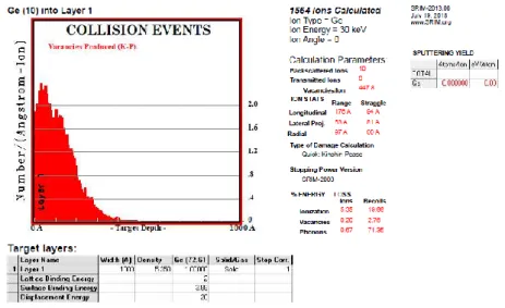
Figure 1. : SRIM simulation showing the vacancy distribution for a Ge recoil of 30 keV.
10
Street [34] has found that the presence of disorders in amorphous silicon enhances the cross section for the capture of carriers by the defects. Later, an analytical model has been developed that clearly explains this effect using simple assumptions [33]. This mitigates the direct role of disordered regions as being the sole origin of carrier capture at 77 K. The sizes of these disordered regions is of the order of the range of primary recoil atoms (Figure 1.). Isolated defects should contribute greatly to the trapping process. The recoil of an atom is induced by the collision with the impinging particle. SRIM simulations show that its range is of the order of 10 nm at 10-30 keV, with around a few hundred vacancies being created on its trajectory. The recoil energy has been computed for neutrons in the MeV energy range, see Figure 1. In most cases, a thermal treatment above room temperature is used to remove radiation damage. In reference [31] recombination-enhanced annealing using minority-carrier injection was applied but with no significant results, at least at room temperature. At low temperature, when the defects are not stable, no improvement could be observed with this method. However, a strong dependence of the annealing stages on the material type (p or n) was observed in references [3] [25] and other detector studies.
3.4. Alternatives to HPGe
For a long time, materials alternative to HPGe have been proposed and corresponding detectors were fabricated. We can cite as an example GaAs (mostly for X-ray detection), and, more importantly, CdTe. The goal was to eliminate the need for cryogenic operation by the use of large bandgap semi-insulating material (diamond is also considered). Many difficulties still exist, mostly related to the defect density that is much higher in binary materials [9]. The other drawback is the possibility to grow large crystals, which proves to be more difficult for alternative materials. Large diamond single crystals with a low nitrogen content are difficult to grow as they need high-pressure processing. However, some CdTe photon detectors using segmented crystals for photon identification have been successfully implemented on space missions (INTEGRAL) [24], Segmentation allows reducing drift length and therefore trapping so that the resolution can be maintained at an acceptable level.
3.5. Particle identification
Particle identification through pulse shape discrimination is one of the developments that are used mainly in nuclear physics [35]. These techniques can be adequately used to determine the region of the detector where the interaction took place. There have been early reports for methods of particle identification in germanium and silicon detectors [36] [37] The detection of photons is basically
through ionisation and there is no important interaction with the nucleus, which could transfer momentum to the nucleus. If we consider other particles with a significant mass, their interaction with the nucleus may induce a recoil, which in turn is slowed down in the detector material. The slowing-down process results in ionization (electron-hole pairs generation), defect creation (vacancies and interstitials), and phonon creation. One should note that according to SRIM simulations, in the typical energy range for the recoil (20-30 keV) the most important contribution (73 %) is from phonon emission. The energy used for vacancy creation is of the order of 3%, which indicates that defect monitoring [38] could provide an alternative way to estimate the total integrated flux of interacting particles, since when stable defects are created, their concentration is proportional to the total number of interacting particles in a given time interval, which can be very long. The rest of the energy is used for ionisation (25 %). This result is close to the experimental result obtained for cryogenic detectors, as it will be discussed in the paragraph on dark matter detection.
3.6. Simulation
Simulations of the interaction of photons with matter have been given a certain attention. Monte Carlo codes have been developed. Recently the NWEGRIM code [18] from Pacific Northwest laboratories has been used to simulate the interaction of photons in silicon, but these simulations could also be applied to germanium. GEANT4 has been used for simulation of charged particles interacting with germanium [39].
4. Gamma-ray tracking arrays
High-purity germanium γ-ray tracking arrays, such as AGATA (Advanced GAmma Tracking Array) [40] and GRETINA/GRETA (Gamma Ray Energy Tracking Array) [41] represent the state-of-the-art in high-resolution γ-ray spectroscopy for nuclear physics experiments. These spectrometers are composed of highly segmented large-volume HPGe crystals. Pulse-shape analysis, applied to the recorded signals from the segments, yields three-dimensional interaction positions with a typical precision of about 2mm [40] [41]. Subsequently, a γ-ray tracking algorithm is applied to the determined interaction points in order to group and order them in sequences corresponding to individual γ rays. In this procedure, the geometrical criteria and the Compton scattering formula are used, and the full energy of a γ ray is determined as the sum of the energies of the interactions ascribed to the same trajectory.
The γ-ray tracking arrays provide improved energy resolution for in-beam nuclear physics studies thanks to much reduced Doppler broadening as compared to standard γ-ray spectrometers. The use of γ-ray tracking also eliminates the need for Compton-suppression shields, commonly used with HPGe crystals in order to improve the Peak-to-Total ratio. Consequently, the entire 4 solid angle can be
12
be covered with Ge crystals, which leads to significantly increased detection efficiency. The resolving power of a 4 γ-ray tracking array is estimated to be up to two orders of magnitude better than that of the existing conventional γ-ray spectrometers, depending on the physics case [41]. This is particularly important for studies of very exotic nuclei far from stability, employing weak radioactive-ion beams at intermediate energies (up to several hundred MeV/u), which leads to recoil velocities that may exceed 30% of the speed of light [42].
5. Dark matter direct detection and related studies
The last two decades have seen an important effort devoted to search for Dark Matter, using Underground Direct Detection Apparatus [37] [36] [43] [44] [45] [46] [47]. The first stage was to design a detector able to discriminate between particles in order to identify the so-called Weakly Interacting Massive Particles that are thought to be a constituent of Dark Matter. The developed detectors include two channels: a ‘thermal ‘channel which is based on the thermalization of phonons, and a ionisation channel which is proportional to the number of carriers collected. In reality the so-called Luke-Neganov effect [48] [49] affects the properties of the detector. The Luke-Neganov effect consists in the amplification of the phonon signal by the electron (carrier) drift [50].
The charge signal may be expressed as: sc=
E
εq , where E is the average energy for electron-hole pair creation, and
𝐬𝐓=
E
εqV + E
The ST term is proportional to the charge multiplied by the voltage drop, so we can write that, if t is the time necessary for the charge to be collected:
I = Sc/t
First term: ItV which is a Joule-like term. Energy=Power x time= current x voltage x time = charge x voltage.
These relations indicate the need to operate at weak field if we want to reduce the contribution of the phonon signal. At high fields, the phonon signal tends to grow linearly with the applied voltage. Of course, the heat signal can only be detected if the calorific capacity is low enough, and so the operating temperature should be very low. This is the reason behind the use of cryogenic (mK range) germanium bolometers. Another reason why the germanium is chosen is that it has more nucleons, which should enhance interaction cross sections of WIMPS with the detecting medium. If we consider the interaction of fast neutrons with germanium (in the MeV range) as an example, the elastic-scattering cross section is much higher than the inelastic cross section [31] and is of the order of 3 barns [5]. Hence, the mean free path of these fast neutrons is close to a few
centimetres. The recoil nucleus with an energy of a few tens of keV dissipates 25% of its energy into ionisation, which amounts to a few keV (5 keV). The ionization channel monitors this fraction of energy. A similar phenomenon was observed, but not published, in planar HPGe 77 K detectors exposed to neutrons in the MeV range [51]. The heat channel monitors almost entire energy deposited by the recoils, except for the fraction needed for vacancy-interstitial (defect) creation. If a neutron is totally absorbed in the bolometer following multiple scattering, the total energy of all recoils matches the initial energy of the impinging neutron, and therefore the heat channel signal reflects the total energy deposited.
Figure 2. Diagram showing the energy of the trapping level in Ge band gap versus temperature, using a simple Boltzmann factor. This is valid at high temperature for thermal emission with a time constant Tau. The region investigated by DLTS is delimited by the upper square on the right. The purple arrow shows the operation of DM cryogenic experiments such as EDELWEISS.
The calibration runs yielded the ratio of the ionization signal to the phonon energy equal to 30%. This is very close to the value of 25%/73% =0.35 determined in a SRIM simulation. When the particle interacts with matter purely via ionization, as it is the case for photons, the ratio of ionizing energy to the total energy is close to one, if no Luke-Neganov amplifying occurs. Therefore, this configuration can be used for particle discrimination [46]. For the WIMPS experiments, if we consider that these particles interact with the nuclei of the detecting media, this provides a way of discriminating the photons from other
14
events. At this cryogenic energy (a few mK), the shallow and deep levels may disturb the charge transport through the detector (Figure 2). This is the reason why the detector is saturated with photo-generated carriers prior to data acquisition. In spite of this, more detailed defect studies on the starting material should be made [52]. In particular, as very shallow levels may have an impact, the non-thermal carrier emission or capture should be studied. Additionally a method using alternately biased electrodes on each surface of the detectors, including the sides, has enabled the measurement of volume-only events, eliminating near-surface events related to low-energy particles strongly interacting with the medium [46]. Other techniques have been developed [53] to solve this problem.
6. Conclusion
This short review provides an overview of HPGe detectors and their applications in physics [23] [45] and outside it. The future of such detectors depends on the availability of other materials that would match the resolution performance of HPGe at 77K, while operating at room temperature. Segmentation of the detectors provides a way to reduce carrier collection lengths and hence to mitigate the effects of electrically active deep defects. With integrated microelectronics the noise can be as low as a few tens of electrons. With on detectors CMOS chips and low capacitance detectors the electronic noise can be reduced to less than 100 e-h pairs. With equal to 4.5 eV (GaAs,CdTe) , this corresponds to a resolution of the order of 450 eV. This could also be applied to HPGe detectors that are being used for double beta decay or Dark Matter experiments. The multi-electrode scheme that is implemented in EDELWEISS III [46] is a first step towards a time-projection chamber HPGe detector allowing an improved discrimination ability. Each electrode could be a separate channel, which would be easy for the detector operated at low field and low voltage. It seems clear that the use in more routine applications such as for instance high-precision radioactive material characterization and radioactive material tracing to avoid nuclear dissemination will remain a field where HPGe is the most competitive, despite the need for LN2 cryogenic installations. Development of cryogenic cooling fridges will eliminate this specific constraint. In scientific applications, HPGe, being one of the chemically purest materials ever fabricated, will remain to be needed.
Acknowledgments
The contribution of researchers from IRFU and other institutions, with whom the first author had fruitful discussions while working on Dark Matter instrumentation, is gratefully acknowledged.
Conflict of Interest
References
[1] R. D. Baertsch and R. N. Hall, "Gamma Ray Detectors Made from High Purity Germanium," IEEE Transactions on Nuclear Science, vol. 17, pp. 235-240, 6 1970.
[2] E. E. Haller, W. L. Hansen and F. S. Goulding, "Physics of ultra-pure germanium," Advances in Physics, vol. 30, pp. 93-138, 1981.
[3] N. Fourches, G. Walter and J. C. Bourgoin, "Neutron-induced defects in high-purity germanium," Journal of applied physics, vol. 69, pp. 2033-2043, 1991. [4] R. C. Alig and S. Bloom, "Electron-Hole-Pair Creation Energies in
Semiconductors," Phys. Rev. Lett., vol. 35, no. 22, pp. 1522-1525, 12 1975. [5] R. C. Alig, S. Bloom and C. W. Struck, "Electron-hole-pair creation energies in semiconductors," in BULLETIN OF THE AMERICAN PHYSICAL SOCIETY, 1980.
[6] R. C. Alig, S. Bloom and C. W. Struck, "Scattering by ionization and phonon emission in semiconductors," Physical Review B, vol. 22, p. 5565, 1980. [7] R. C. Alig, "Scattering by ionization and phonon emission in semiconductors.
II. Monte Carlo calculations," Physical Review B, vol. 27, p. 968, 1983. [8] C. A. Klein, "Bandgap dependence and related features of radiation
ionization energies in semiconductors," Journal of Applied Physics, vol. 39, pp. 2029-2038, 1968.
[9] G. Bertolini, F. Cappellani and G. Restelli, "Current state of the art in semiconductor detectors," Nuclear Instruments and Methods, vol. 112, pp. 219-228, 1973.
[10] L. Campbell, F. Gao, R. Devanathan and W. J. Weber, "Model of plasmon decay for electron cascade simulation," Nuclear Instruments and Methods
in Physics Research Section A: Accelerators, Spectrometers, Detectors and Associated Equipment, vol. 579, pp. 454-457, 2007.
[11] G. L. Miller, B. D. Pate and S. Wagner, "Production of Thick Semiconductor Radiation Detectors by Lithium Drifting," IEEE Transactions on Nuclear
Science, vol. 10, pp. 220-229, 1963.
[12] R. N. Hall, "Characterization of Pure Germanium for Detector Fabrication,"
IEEE Transactions on Nuclear Science, vol. 19, pp. 266-270, 6 1972.
[13] S. J. Pearton, "Hydrogen passivation of copper-related defects in germanium," Applied Physics Letters, vol. 40, pp. 253-255, 1982.
16
[14] G. Wang, H. Mei, D. Mei, Y. Guan and G. Yang, "High purity germanium crystal growth at the University of South Dakota," in Journal of Physics:
Conference Series, 2015.
[15] K. A. Olive, P. D. Group and others, "Review of particle physics," Chinese
Physics C, vol. 38, p. 090001, 2014.
[16] G. Nelson and D. Reilly, "Gamma-ray interactions with matter," Passive
nondestructive analysis of nuclear materials, pp. 27-42, 1991.
[17] E. Sakai, "Recent topics in semiconductor detector development," 1978. [18] F. Gao, L. W. Campbell, R. Devanathan, Y. Xie, L. R. Corrales, A. J. Peurrung
and W. J. Weber, "Monte Carlo method for simulating γ-ray interaction with materials: A case study on Si," Nuclear Instruments and Methods in Physics
Research Section A: Accelerators, Spectrometers, Detectors and Associated Equipment, vol. 579, pp. 292-296, 2007.
[19] C. Cetina, B. L. Berman, W. J. Briscoe, P. L. Cole, G. Feldman, P. Heimberg, L. Y. Murphy, S. A. Philips, J. C. Sanabria, H. Crannell and others, "Photofission of heavy nuclei at energies up to 4 GeV," Physical review letters, vol. 84, p. 5740, 2000.
[20] T. Behnke, "The international linear collider technical design report-volume 4: detectors," 2013.
[21] U. Fano, "Ionization yield of radiations. II. The fluctuations of the number of ions," Physical Review, vol. 72, p. 26, 1947.
[22] U. Fano, "On the theory of ionization yield of radiations in different substances," Physical Review, vol. 70, p. 44, 1946.
[23] D. L. Upp, R. M. Keyser and T. R. Twomey, "New cooling methods for HPGE detectors and associated electronics," Journal of Radioanalytical and
Nuclear Chemistry, vol. 264, pp. 121-126, 01 3 2005.
[24] F. Lebrun, J. P. Leray, P. Lavocat, J. Crétolle, M. Arques, C. e. Blondel, C. Bonnin, A. Bouere, C. Cara, T. Chaleil and others, "ISGRI: The INTEGRAL soft gamma-ray imager," Astronomy & Astrophysics, vol. 411, pp. L141--L148, 2003.
[25] N. Fourches, A. Huck and G. Walter, "The role of secondary defects in the loss of energy resolution of fast-neutron-irradiated HPGe gamma-ray detectors," IEEE transactions on nuclear science, vol. 38, pp. 1728-1735, 1991.
[26] R. B. Bernstein and D. Cubicciotti, "The Kinetics of the Reaction of Germanium and Oxygen," Journal of the American Chemical Society, vol. 73, pp. 4112-4114, 1951.
[27] B. Onsia, T. Conard, S. De Gendt, M. Heyns, I. Hoflijk, P. Mertens, M. Meuris, G. Raskin, S. Sioncke, I. Teerlinck and others, "A study of the influence of typical wet chemical treatments on the germanium wafer surface," Solid
State Phenomena, vol. 103, pp. 27-30, 2005.
[28] M. Kobayashi, G. Thareja, M. Ishibashi, Y. Sun, P. Griffin, J. McVittie, P. Pianetta, K. Saraswat and Y. Nishi, "Radical oxidation of germanium for interface gate dielectric GeO 2 formation in metal-insulator-semiconductor gate stack," Journal of Applied Physics, vol. 106, p. 104117, 2009.
[29] A. Delabie, F. Bellenger, M. Houssa, T. Conard, S. Van Elshocht, M. Caymax, M. Heyns and M. Meuris, "Effective electrical passivation of Ge(100) for high-k gate dielectric layers using germanium oxide," Applied Physics
Letters, vol. 91, p. 082904, 2007.
[30] R. H. Pehl, N. W. Madden, J. H. Elliott, T. W. Raudorf, R. C. Trammell and L. S. Darken, "Radiation Damage Resistance of Reverse Electrode GE Coaxial Detectors," IEEE Transactions on Nuclear Science, vol. 26, pp. 321-323, 2 1979.
[31] N. Fourches, "Etude des defauts dus a l'irradiation aux neutrons rapides dans le germanium de haute purete," 1989.
[32] S. M. Kogan and T. M. Lifshits, "Photoelectric Spectroscopy _ A New Method of Analysis of Impurities in Semiconductors," physica status solidi (a), vol. 39, pp. 11-39.
[33] N. Fourches, "High defect density regions in neutron irradiated high-purity germanium: Characteristics and formation mechanisms," Journal of applied
physics, vol. 77, pp. 3684-3689, 1995.
[34] R. A. Street, "Disorder effects on deep trapping in amorphous semiconductors," Philosophical Magazine B, vol. 49, pp. L15--L20, 1984. [35] A. Pullia, G. Pascovici, B. Cahan, D. Weisshaar, C. Boiano, R. Bassini, M. Petcu
and F. Zocca, "The AGATA charge-sensitive preamplifiers with built-in active-reset device and pulser," in Nuclear Science Symposium Conference
Record, 2004 IEEE, 2004.
[36] T. Shutt, B. Ellman, P. D. Barnes Jr, A. Cummings, A. Da Silva, J. Emes, Y. Giraud-Héraud, E. E. Haller, A. E. Lange, R. R. Ross and others, "Measurement of ionization and phonon production by nuclear recoils in a
18
60 g crystal of germanium at 25 mK," Physical review letters, vol. 69, p. 3425, 1992.
[37] G. Gerbier, E. Lesquoy, J. Rich, M. Spiro, C. Tao, D. Yvon, S. Zylberajch, P. Delbourgo, G. Haouat, C. Humeau and others, "Measurement of the ionization of slow silicon nuclei in silicon for the calibration of a silicon dark-matter detector," Physical Review D, vol. 42, p. 3211, 1990.
[38] R. Budnik, O. Cheshnovsky, O. Slone and T. Volansky, "Direct detection of light dark matter and solar neutrinos via color center production in crystals," Physics Letters B, vol. 782, pp. 242-250, 2018.
[39] N. T. Fourches and R. Chipaux, "Electrical-modelling, design and simulation of cumulative radiation effects in semiconductor pixels detectors: prospects and limits," Journal of Instrumentation, vol. 10, p. C01036, 2015.
[40] S. Akkoyun, A. Algora, B. Alikhani, F. Ameil, G. De Angelis, L. Arnold, A. Astier, A. Ataç, Y. Aubert, C. Aufranc and others, "Agata—advanced gamma tracking array," Nuclear Instruments and Methods in Physics Research
Section A: Accelerators, Spectrometers, Detectors and Associated Equipment, vol. 668, pp. 26-58, 2012.
[41] S. Paschalis, I. Y. Lee, A. O. Macchiavelli, C. M. Campbell, M. Cromaz, S. Gros, J. Pavan, J. Qian, R. M. Clark, H. L. Crawford and others, "The performance of the gamma-ray energy tracking in-beam nuclear array GRETINA," Nuclear
Instruments and Methods in Physics Research Section A: Accelerators, Spectrometers, Detectors and Associated Equipment, vol. 709, pp. 44-55,
2013.
[42] D. Weisshaar, D. Bazin, P. C. Bender, C. M. Campbell, F. Recchia, V. Bader, T. Baugher, J. Belarge, M. P. Carpenter, H. L. Crawford and others, "The performance of the γ-ray tracking array GRETINA for γ-ray spectroscopy with fast beams of rare isotopes," Nuclear Instruments and Methods in
Physics Research Section A: Accelerators, Spectrometers, Detectors and Associated Equipment, vol. 847, pp. 187-198, 2017.
[43] R. J. Creswick, F. T. Avignone III, H. A. Farach, J. I. Collar, A. O. Gattone, S. Nussinov and K. Zioutas, "Theory for the direct detection of solar axions by coherent Primakoff conversion in germanium detectors," Physics Letters B, vol. 427, pp. 235-240, 1998.
[44] R. Essig, J. Mardon, O. Slone and T. Volansky, "Detection of sub-GeV dark matter and solar neutrinos via chemical-bond breaking," Physical Review D, vol. 95, p. 056011, 2017.
[45] I. Abt, A. Caldwell, D. Gutknecht, K. Kr_ninger, M. Lampert, X. Liu, B. Majorovits, D. Quirion, F. Stelzer and P. Wendling, "Characterization of the first true coaxial 18-fold segmented n-type prototype HPGe detector for the
gerda project," Nuclear Instruments and Methods in Physics Research
Section A: Accelerators, Spectrometers, Detectors and Associated Equipment, vol. 577, pp. 574-584, 2007.
[46] E. Armengaud, Q. Arnaud, C. Augier, A. Benoı ̂t, L. Bergé, T. Bergmann, J. Billard, T. De Boissière, G. Bres, A. Broniatowski and others, "Performance of the EDELWEISS-III experiment for direct dark matter searches," Journal
of Instrumentation, vol. 12, p. P08010, 2017.
[47] E. Armengaud, C. Augier, A. Benoit, L. Bergé, T. Bergmann, J. Blümer, A. Broniatowski, V. Brudanin, B. Censier, M. Chapellier and others, "Search for low-mass WIMPs with EDELWEISS-II heat-and-ionization detectors,"
Physical Review D, vol. 86, p. 051701, 2012.
[48] P. N. Luke, "Voltage-assisted calorimetric ionization detector," Journal of
Applied Physics, vol. 64, pp. 6858-6860, 1988.
[49] B. S. Neganov and V. N. Trofimov, "USSR Patent No 1037771 (1985)
[50] P. Di Stefano, "Recherche de matière sombre non-baryonique au moyen d'un bolomètre à ionisation dans le cadre de l'expérience EDELWEISS," 1998.
[51] A. Huck, 1989, CRN, Strasbourg, private communication, with Nicolas Fourches
[52] J. Domange, E. Olivieri, N. Fourches and A. Broniatowski, "Thermally-Stimulated Current Investigation of Dopant-Related D- and A+ Trap Centers in Germanium for Cryogenic Detector Applications," Journal of Low
Temperature Physics, vol. 167, pp. 1131-1136, 2012.
[53] L. T. Yang, H. B. Li, H. T. Wong, M. Agartioglu, J. H. Chen, L. P. Jia, H. Jiang, J. Li, F. K. Lin, S. T. Lin and others, "Bulk and surface event identification in p-type germanium detectors," Nuclear Instruments and Methods in Physics
Research Section A: Accelerators, Spectrometers, Detectors and Associated Equipment, vol. 886, pp. 13-23, 2018.