Publisher’s version / Version de l'éditeur:
Nanomaterials, 7, 5, p. 95, 2017-04-29
READ THESE TERMS AND CONDITIONS CAREFULLY BEFORE USING THIS WEBSITE. https://nrc-publications.canada.ca/eng/copyright
Vous avez des questions? Nous pouvons vous aider. Pour communiquer directement avec un auteur, consultez la première page de la revue dans laquelle son article a été publié afin de trouver ses coordonnées. Si vous n’arrivez pas à les repérer, communiquez avec nous à [email protected].
Questions? Contact the NRC Publications Archive team at
[email protected]. If you wish to email the authors directly, please see the first page of the publication for their contact information.
Archives des publications du CNRC
This publication could be one of several versions: author’s original, accepted manuscript or the publisher’s version. / La version de cette publication peut être l’une des suivantes : la version prépublication de l’auteur, la version acceptée du manuscrit ou la version de l’éditeur.
For the publisher’s version, please access the DOI link below./ Pour consulter la version de l’éditeur, utilisez le lien DOI ci-dessous.
https://doi.org/10.3390/nano7050095
Access and use of this website and the material on it are subject to the Terms and Conditions set forth at
One-dimensional electron transport layers for perovskite solar cells
Thakur, Ujwal; Kisslinger, Ryan; Shankar, Karthik
https://publications-cnrc.canada.ca/fra/droits
L’accès à ce site Web et l’utilisation de son contenu sont assujettis aux conditions présentées dans le site
LISEZ CES CONDITIONS ATTENTIVEMENT AVANT D’UTILISER CE SITE WEB.
NRC Publications Record / Notice d'Archives des publications de CNRC:
https://nrc-publications.canada.ca/eng/view/object/?id=7f09f3e3-454d-4ec3-b7a9-e9c8e85c5615 https://publications-cnrc.canada.ca/fra/voir/objet/?id=7f09f3e3-454d-4ec3-b7a9-e9c8e85c5615nanomaterials
Review
One-Dimensional Electron Transport Layers for
Perovskite Solar Cells
Ujwal K. Thakur1,*,†, Ryan Kisslinger1,†and Karthik Shankar1,2
1 Department of Electrical and Computer Engineering, University of Alberta,
Edmonton, AB T6G 1H9, Canada; [email protected] (R.K.); [email protected] (K.S.) 2 National Research Council, National Institute for Nanotechnology, 11421 Saskatchewan Drive NW,
Edmonton, AB T6G 2M9, Canada
* Correspondence: [email protected]; Tel.: +1-780-492-1354 † These authors contributed equally.
Academic Editor: Shuangqiang Chen
Received: 12 February 2017; Accepted: 24 April 2017; Published: 29 April 2017
Abstract:The electron diffusion length (Ln) is smaller than the hole diffusion length (Lp) in many halide perovskite semiconductors meaning that the use of ordered one-dimensional (1D) structures such as nanowires (NWs) and nanotubes (NTs) as electron transport layers (ETLs) is a promising method of achieving high performance halide perovskite solar cells (HPSCs). ETLs consisting of oriented and aligned NWs and NTs offer the potential not merely for improved directional charge transport but also for the enhanced absorption of incoming light and thermodynamically efficient management of photogenerated carrier populations. The ordered architecture of NW/NT arrays affords superior infiltration of a deposited material making them ideal for use in HPSCs. Photoconversion efficiencies (PCEs) as high as 18% have been demonstrated for HPSCs using 1D ETLs. Despite the advantages of 1D ETLs, there are still challenges that need to be overcome to achieve even higher PCEs, such as better methods to eliminate or passivate surface traps, improved understanding of the hetero-interface and optimization of the morphology (i.e., length, diameter, and spacing of NWs/NTs). This review introduces the general considerations of ETLs for HPSCs, deposition techniques used, and the current research and challenges in the field of 1D ETLs for perovskite solar cells.
Keywords:photovoltaics; ordered bulk heterojunctions; solution processing; light scattering; surface traps; electrochemical anodization; solvothermal synthesis; metal oxide; TiO2; ZnO
1. Introduction
The increasing global demand for energy has spurred research efforts to find new and improved sources of cheap, environmentally neutral, renewable energy. Inorganic solar cells based on materials such as crystalline silicon, cadmium telluride, or copper indium germanium selenide (CIGS) constitute mature technologies that exhibit a relatively high power conversion efficiency (PCE) of around 12%–20% in deployed modules [1] and thus dominate commercially available photovoltaic technologies. However, the relatively long energy payback times of inorganic solar cells [2,3] have partially impeded their pace to widespread deployment, and thus alternative approaches are being explored. Organic photovoltaics [4], dye-sensitized solar cells [5], halide perovskite solar cells [6], and quantum-dot solar cells [7] are examples of next generation solution-processable solar cell technologies that have emerged as lower cost, lower energy payback time alternatives to replace conventional solar cells [8,9]. Among these technologies, halide perovskite solar cells (HPSCs) are currently the topic of intense scientific and engineering interest due to their facile synthesis, use of earth-abundant constituent elements and high device performance [10]. A major breakthrough occurred in 2012 when
Snaith et al. [11] reported an HPSC device with a PCE of 11% using a mixed halide perovskite layer (CH3NH3PbI3−xClx) as the active layer on nanoporous aluminum oxide. The first report of a HPSC was by Miyasaka and co-workers, who obtained a PCE of 3.8% in 2009 [12] using an active layer consisting of CH3NH3PbI3(henceforth referred to as MAPbI3).
Perovskites, named after the Russian mineralogist Lev A. Perovski, are compounds having the molecular formula ABX3and a specific crystal structure consisting of A and B cations together with X anions arranged in a cubic array of BX6 octahedra sharing corners, with the A cations placed in the cuboctahedral interstices which belong to the cubic Pm3m crystal structure as shown in Figure1[13]. In halide perovskites, X is a halide ion while A is a monovalent ion such as Cs+, CH3NH3+(MA), or NH=CHNH3+, and B is a divalent ion such as Pb2+or Sn2+. Unlike oxide perovskites, halide perovskites are not strictly ionic since the bond between the Group IV metal atom and the halide atom has some covalent character, which is maximum for iodide perovskites.
performance [10]. A major breakthrough occurred in 2012 when Snaith et al. [11] reported an HPSC device with a PCE of 11% using a mixed halide perovskite layer (CH3NH3PbI3−xClx) as the active layer on nanoporous aluminum oxide. The first report of a HPSC was by Miyasaka and co-workers, who obtained a PCE of 3.8% in 2009 [12] using an active layer consisting of CH3NH3PbI3(henceforth
referred to as MAPbI3).
Perovskites, named after the Russian mineralogist Lev A. Perovski, are compounds having the molecular formula ABX3and a specific crystal structure consisting of A and B cations together with
X anions arranged in a cubic array of BX6 octahedra sharing corners, with the A cations placed in the cuboctahedral interstices which belong to the cubic Pm3m crystal structure as shown in Figure 1 [13]. In halide perovskites, X is a halide ion while A is a monovalent ion such as Cs+, CH
3NH3+(MA),
or NH=CHNH3+, and B is a divalent ion such as Pb2+ or Sn2+. Unlike oxide perovskites, halide
perovskites are not strictly ionic since the bond between the Group IV metal atom and the halide atom has some covalent character, which is maximum for iodide perovskites.
Figure 1. Schematic of cubic metal halide perovskites with the composition ABX3, with A =
Univalent alkali metal cation (shown in green), B = Group IV metal cation (shown in grey) and X = halide ion (shown in purple). Reprinted with permission from Macmillan Publishers Ltd.: Nature Materials Ref. [14], Copyright 2014.
Halide perovskites have unique properties [15] such as a direct optical bandgap, broadband light absorption, low carrier effective masses, dominant shallow point defects, benign grain boundaries, ambipolar transport, and long carrier diffusion lengths, due to which they have been investigated as light-absorbing and charge transporting materials in photovoltaic devices. In an astonishingly short period, this has led to an as-of-yet highest power conversion efficiency of 21.1% [16]. The highest efficiencies reported thus far, have been obtained using iodide perovskites, and mixed iodide-bromide perovskites. One challenge associated with perovskite solar cells is the choice of electron transport layer (ETL) in the solar cell architecture. It is important for the ETL to possess certain properties including an appropriate work function, high conductivity, fast charge transport, and a low recombination rate at the interface. Both inorganic and organic semiconductors have been used, with TiO2being the most commonly used and having seen the most success. The
morphology of the ETL layer is also of importance with planar film layers, mesoscopic particulate layers, and nanostructured layers being used. Planar film layers, while being the easiest to fabricate, are required to have a sufficient thickness in order to absorb all of the incident solar light. This thickness, however, is usually required to be longer than the diffusion length of electrons, which has been measured to be 100 nm or higher in iodide perovskites [17]. Mesoscopic electron transport layers have the advantage of allowing for infiltration of the perovskite, meaning that any dimension of the perovskite is kept to a minimum while still being able to absorb all the sun’s incident light [18]. However, it can be very difficult to completely fill the pore network of a mesoscopic structure with perovskite, and any unfilled areas inevitably lead to recombination at the exposed surfaces. In addition, a mesoscopic structure consisting of an interconnected network of nanoparticles, results in
Figure 1.Schematic of cubic metal halide perovskites with the composition ABX3, with A = Univalent alkali metal cation (shown in green), B = Group IV metal cation (shown in grey) and X = halide ion (shown in purple). Reprinted with permission from Macmillan Publishers Ltd.: Nature Materials Ref. [14], Copyright 2014.
Halide perovskites have unique properties [15] such as a direct optical bandgap, broadband light absorption, low carrier effective masses, dominant shallow point defects, benign grain boundaries, ambipolar transport, and long carrier diffusion lengths, due to which they have been investigated as light-absorbing and charge transporting materials in photovoltaic devices. In an astonishingly short period, this has led to an as-of-yet highest power conversion efficiency of 21.1% [16]. The highest efficiencies reported thus far, have been obtained using iodide perovskites, and mixed iodide-bromide perovskites. One challenge associated with perovskite solar cells is the choice of electron transport layer (ETL) in the solar cell architecture. It is important for the ETL to possess certain properties including an appropriate work function, high conductivity, fast charge transport, and a low recombination rate at the interface. Both inorganic and organic semiconductors have been used, with TiO2being the most commonly used and having seen the most success. The morphology of the ETL layer is also of importance with planar film layers, mesoscopic particulate layers, and nanostructured layers being used. Planar film layers, while being the easiest to fabricate, are required to have a sufficient thickness in order to absorb all of the incident solar light. This thickness, however, is usually required to be longer than the diffusion length of electrons, which has been measured to be 100 nm or higher in iodide perovskites [17]. Mesoscopic electron transport layers have the advantage of allowing for infiltration of the perovskite, meaning that any dimension of the perovskite is kept to a minimum while still being able to absorb all the sun’s incident light [18]. However, it can be very difficult to completely fill the pore network of a mesoscopic structure with perovskite, and any unfilled areas inevitably lead to recombination at the exposed surfaces. In addition, a mesoscopic
Nanomaterials 2017, 7, 95 3 of 27
structure consisting of an interconnected network of nanoparticles, results in non-directional electron transport involving a random walk [19]. One dimensional nanostructures (1D-NS), however, are able to lever the same advantages of mesoscopic structures, while being able to allow for a more complete infiltration of perovskite into the electron transporting layer. Furthermore, their directional charge transport properties enable increased solar cell efficiencies [20–23]. In addition, 1D-NS with optimized geometries enable the improved management of incident photons in the solar cell. This review aims to summarize the fundamentals of preparing perovskite solar cells and how they relate to using one-dimensional electron transport layers (1D-ETLs), with emphasis on TiO2and ZnO nanostructures as the leading candidates. The fundamentals of selecting and fabricating ETLs will be discussed, as well as the special considerations that one has to take into account when dealing with one-dimensional nanostructures. Finally, issues that still need to be solved in order for 1D-NS to achieve commercial viability are addressed.
2. Architecture and Working Mechanism of Devices
As shown in Figure2, perovskite solar cells are fabricated in two major architectures, p-i-n and n-i-p type. In the p-i-n type architecture, a p-type hole transporting layer (HTL) such as CuO, NiO or PEDOT: PSS is deposited on a transparent conductive oxide (TCO) coated glass substrate namely fluorine doped tin oxide (FTO) or indium tin oxide (ITO) coated glasses. This is followed by the deposition of the perovskite active layer which is then coated over by a n-type film of [6,6]-phenyl-C61-butyric acid methyl ester (PCBM), ZnO, or C60 which acts as an ETL and subsequently a low work-function metal such as aluminum is evaporated to complete the device [24–29]. In the n-i-p type architecture, an n-type ETL such as TiO2, ZnO, SnO2or WO3is deposited on a TCO-coated glass substrate which is then followed by perovskite deposition. Over the perovskite, a p-type hole transporting layer (typically spiro-MeOTAD) is deposited and finally a high work function metal such as gold is deposited to complete the device [30–38]. This n-i-p configuration is necessarily used for the formation of solar cells involving 1D-ETLs to allow for proper infiltration of the perovskite into the ETL. Also of note is that ETL-free and HTL-free perovskite solar cells do exist but their photovoltaic performance is low [33,39].
Nanomaterials 2017, 7, 95 3 of 26
non-directional electron transport involving a random walk [19]. One dimensional nanostructures (1D-NS), however, are able to lever the same advantages of mesoscopic structures, while being able to allow for a more complete infiltration of perovskite into the electron transporting layer. Furthermore, their directional charge transport properties enable increased solar cell efficiencies [20–23]. In addition, 1D-NS with optimized geometries enable the improved management of incident photons in the solar cell. This review aims to summarize the fundamentals of preparing perovskite solar cells and how they relate to using one-dimensional electron transport layers (1D-ETLs), with emphasis on TiO2 and ZnO nanostructures as the leading candidates. The
fundamentals of selecting and fabricating ETLs will be discussed, as well as the special considerations that one has to take into account when dealing with one-dimensional nanostructures. Finally, issues that still need to be solved in order for 1D-NS to achieve commercial viability are addressed.
2. Architecture and Working Mechanism of Devices
As shown in Figure 2, perovskite solar cells are fabricated in two major architectures, p-i-n and
n-i-p type. In the p-i-n type architecture, a p-type hole transporting layer (HTL) such as CuO, NiO or
PEDOT: PSS is deposited on a transparent conductive oxide (TCO) coated glass substrate namely fluorine doped tin oxide (FTO) or indium tin oxide (ITO) coated glasses. This is followed by the deposition of the perovskite active layer which is then coated over by a n-type film of [6,6]-phenyl-C61-butyric acid methyl ester (PCBM), ZnO, or C60 which acts as an ETL and
subsequently a low work-function metal such as aluminum is evaporated to complete the device [24–29]. In the n-i-p type architecture, an n-type ETL such as TiO2, ZnO, SnO2or WO3is deposited
on a TCO-coated glass substrate which is then followed by perovskite deposition. Over the perovskite, a p-type hole transporting layer (typically spiro-MeOTAD) is deposited and finally a high work function metal such as gold is deposited to complete the device [30–38]. This n-i-p configuration is necessarily used for the formation of solar cells involving 1D-ETLs to allow for proper infiltration of the perovskite into the ETL. Also of note is that ETL-free and HTL-free perovskite solar cells do exist but their photovoltaic performance is low [33,39].
Figure 2. Layer configuration for (a) p-i-n type and (b) n-i-p type perovskite cell architectures. ETL
and HTL refer to electron transporting layer and hole transporting layer respectively. FTO and ITO refer to fluorine tin oxide coated glass and indium tin oxide coated glass respectively
3. Halide Perovskite Deposition Techniques
The performance of perovskite solar cells is highly dependent on the crystal structure and morphology of the perovskite absorber, as well as the degree of contact the perovskite makes with the charge transport layers. These factors vary significantly in accordance with the deposition procedure, which should ensure good infiltration and contact when dealing with 1D-ETLs. Furthermore, to prevent direct contact between the electron transporting layer and hole transporting layer, an optimum thickness of perovskite overlayer is needed. This overlayer helps to ensure a sufficiently high value for the shunt resistance. Typically, single step spin coating, two step
Figure 2.Layer configuration for (a) p-i-n type and (b) n-i-p type perovskite cell architectures. ETL and HTL refer to electron transporting layer and hole transporting layer respectively. FTO and ITO refer to fluorine tin oxide coated glass and indium tin oxide coated glass respectively
3. Halide Perovskite Deposition Techniques
The performance of perovskite solar cells is highly dependent on the crystal structure and morphology of the perovskite absorber, as well as the degree of contact the perovskite makes with the charge transport layers. These factors vary significantly in accordance with the deposition procedure, which should ensure good infiltration and contact when dealing with 1D-ETLs. Furthermore, to prevent direct contact between the electron transporting layer and hole transporting layer, an optimum thickness of perovskite overlayer is needed. This overlayer helps to ensure a sufficiently high value
for the shunt resistance. Typically, single step spin coating, two step spin coating, and sequential deposition techniques are used to deposit the active layer in perovskite solar cells. Figure3a is a block diagram of the one step spin casting method which involves the mixing of AX and BX2 in polar solvents such as γ-butyrolactone (GBL), dimethylformamide (DMF) and dimethyl sulfoxide (DMSO) to make the perovskite precursor solution. Spin casting of the precursor solution at sufficient revolutions per minute (RPM) is used to achieve the desired film thickness. This technique generally involves two spinning steps—one at low RPM and another at high RPM. In a typical synthesis, toluene or chlorobenzene is added to the spinning substrate prior to the completion of the second spinning step. After the spin coating step, the substrates are annealed in order to force the crystallization of the deposited perovskite layer. This procedure for perovskite active layer deposition was initially introduced by Miyasaka and coworkers in 2009 and perovskite solar cells with the highest PCEs reported to date employ this technique [12].
Nanomaterials 2017, 7, 95 4 of 26
spin coating, and sequential deposition techniques are used to deposit the active layer in perovskite solar cells. Figure 3a is a block diagram of the one step spin casting method which involves the mixing of AX and BX2in polar solvents such as γ-butyrolactone (GBL), dimethylformamide (DMF)
and dimethyl sulfoxide (DMSO) to make the perovskite precursor solution. Spin casting of the precursor solution at sufficient revolutions per minute (RPM) is used to achieve the desired film thickness. This technique generally involves two spinning steps—one at low RPM and another at high RPM. In a typical synthesis, toluene or chlorobenzene is added to the spinning substrate prior to the completion of the second spinning step. After the spin coating step, the substrates are annealed in order to force the crystallization of the deposited perovskite layer. This procedure for perovskite active layer deposition was initially introduced by Miyasaka and coworkers in 2009 and perovskite solar cells with the highest PCEs reported to date employ this technique [12].
Figure 3. Schematic illustration of (a) one step spin casting (b) sequential deposition (c) two step
spin casting and (d) dual source vapor deposition techniques for perovskite deposition. Adapted from Refs. [40–43] with permission from Macmillan Publishers Ltd. and The Royal Society of Chemistry.
Figure 3b illustrates the methodology of the sequential deposition technique in which BX2 is
dissolved in polar solvents such as DMF and DMSO while another solution of AX is made in 2-propanol. First, BX2is spin coated over the substrate followed by calcination. After cooling down
the substrate to room temperature, it is dipped into AX solution followed by annealing to crystallize the perovskite. The sequential deposition procedure was initially developed by Mitzi and colleagues in 1998 [44] while Gratzel et al. re-introduced this technique to fabricate perovskite
Figure 3.Schematic illustration of (a) one step spin casting (b) sequential deposition (c) two step spin casting and (d) dual source vapor deposition techniques for perovskite deposition. Adapted from Refs. [40–43] with permission from Macmillan Publishers Ltd. and The Royal Society of Chemistry. Figure3b illustrates the methodology of the sequential deposition technique in which BX2is dissolved in polar solvents such as DMF and DMSO while another solution of AX is made in 2-propanol. First, BX2is spin coated over the substrate followed by calcination. After cooling down the substrate to room temperature, it is dipped into AX solution followed by annealing to crystallize the perovskite.
Nanomaterials 2017, 7, 95 5 of 27
The sequential deposition procedure was initially developed by Mitzi and colleagues in 1998 [44] while Gratzel et al. re-introduced this technique to fabricate perovskite solar cells in 2013 [45]. A major problem with this methodology is the length of time needed to convert BX2into ABX3, during which some of the formed ABX3can be leached away from the substrate. Two-step spin coating, illustrated in Figure3c, is a modified version of sequential deposition in which BX2is first spin coated over the substrate followed by calcination. After cooling down the substrate to room temperature AX dissolved in 2-propanol is spin coated over the dry BX2layer. Another important deposition technique that has the ability to produce high performance perovskite solar cells is the dual source vapor deposition technique which was reported in 2013 by Snaith et al. [40]. As shown in Figure3d, AX and BX2are evaporated simultaneously from two different sources in a particular evaporation ratio to form ABX3 film on substrate which is then annealed. Other deposition techniques include sequential vacuum deposition [46], chemical vapor deposition [47], inkjet printing [48,49], spray coating [50,51], and slot die coating [52], but these methods have not been successful thus far in producing high efficiency photovoltaic devices.
4. One Dimensional Nanostructures
1D-NS used in photovoltaics, taking the form of familiar structures such as rods, tubes, and wires, possess two dimensions of a size between 1 and 100 nm while the third dimension is typically in the range 200 nm–1 µm. A wide variety of top-down and bottom-up fabrication approaches exist for their synthesis, with varying degrees of complexity that allow for greater or lesser control over the final structure. Chemical synthesis strategies for 1D-NS are often the cheapest and least demanding in terms of deposition equipment, and include electrodeposition, sol–gel synthesis, solvothermal methods, and electrochemical anodization. While ease of fabrication and relatively high-throughput make these methods attractive options, they often suffer from the drawback of having a greater variability in final properties due to the indirect measures of control inherent to these methods. Strategies based on physical or physicochemical synthesis of 1D-NS such as vapor phase deposition, chemical vapor deposition, vapor-liquid-solid growth, and atomic layer deposition often result in superior electronic properties due to lower impurities and superior crystallinity while requiring dedicated deposition equipment and extreme conditions such as high vacuum and/or elevated temperatures. Even more precise control over the final structure can be obtained by techniques such as electron beam lithography or focused-ion beam writing or x-ray lithography, although these processes are much more expensive and of low-throughput.
Several studies have found that the diffusion length of photogenerated electrons in halide perovskites is lower than that of photogenerated holes as shown in Figure4, which calls for the application of nanostructured ETLs in perovskite solar cells [53,54]. 1D-NS offer a large surface area and the possibility of confinement of phonons and charge carriers, which leads to distinct electrical, optical and structural properties when contrasted with those of bulk materials. They may be used to limit the “random walk” of charges through a material; as there is only one direction in which charges may travel, the overall length of the path a charge takes on its way to being collected is reduced and thus charge recombination is limited. It is also important to use an optimized thickness of ETLs in perovskite solar cells (corresponding to the length of 1D ETL nanostructures). Because most perovskite semiconductors used in solar cells have a high extinction coefficient, an increase in the thickness of 1D ETLs does not generally improve the overall absorption of the device. However, increasing the thickness of 1D ETLs can reduce the photovoltaic performance of perovskite solar cells. The open circuit voltage decreases as the nanostructure length increases because of increased recombination at the ETL/perovskite interface [55–57]. The short circuit current too typically decreases because of ultraviolet photons absorbed by thicker ETLs which cannot be transmitted to the perovskite absorber layer [55,58]. The fill factor also reduces because of an increased series resistance of the solar cell. On the other hand, too thin an ETL does not provide a sufficient mesoscopic effect. If left unoptimized, forward- and back-scattering due to thick nanostructured ETLs can outcouple incident photons out of
the device and reduce the amount of light harvested [59]. The nanorod packing density in 1D ETLs is another important parameter which plays a crucial role in the photovoltaic performance of solar cells. If the nanorods are densely packed, then there is less room between adjacent nanorods/nanotubes for the perovskite to be filled, resulting in poor filling and lower photovoltaic performance of the solar cells. Moderate and low density packing of the nanorods constituting the 1D ETL provide better filling and thus improved light harvesting efficiency [60–62]. Thus, it is important to optimize the thickness and morphology of 1D ETLs to take proper advantage of their directional charge transport and light management properties without harming other performance parameters of the solar cell. For high aspect ratio nanorods in the ETL, field emission of electrons into the perovskite is promoted, which in turn, may increase the dark current in the solar cells and thereby reduce the Vocvalue [59]. A superficial coating of perovskite is favored for high aspect ratio NRs with polar surfaces due to wetting considerations, as opposed to volumetric filling of the inter-rod spaces, which can exacerbate problems with extracting holes.
Nanomaterials 2017, 7, 95 6 of 26
filling and lower photovoltaic performance of the solar cells. Moderate and low density packing of the nanorods constituting the 1D ETL provide better filling and thus improved light harvesting efficiency [60–62]. Thus, it is important to optimize the thickness and morphology of 1D ETLs to take proper advantage of their directional charge transport and light management properties without harming other performance parameters of the solar cell. For high aspect ratio nanorods in the ETL, field emission of electrons into the perovskite is promoted, which in turn, may increase the dark current in the solar cells and thereby reduce the Voc value [59]. A superficial coating of perovskite is favored for high aspect ratio NRs with polar surfaces due to wetting considerations, as opposed to volumetric filling of the inter-rod spaces, which can exacerbate problems with extracting holes.
Figure 4. Time-resolved photoluminescence (along with stretched exponential fits) of MAPbI3using
the electron quencher [6,6]-phenyl-C61-butyric acid methyl ester (PCBM) shown as blue trianges or
using the hole quencher layer Spiro-MeOTAD, shown as red circles. The data obtained without the use of a quencher, instead using insulating polymer poly(methylmethacrylate) (PMMA) is shown as black squares. Adapted from Ref. [53] with permission from The American Association for the Advancement in Science.
5. Materials for One Dimensional Electron Transport Layers
Both inorganic and organic semiconductors have been used as electron transport materials, although it is inorganic materials that have received attention for their applicability as one-dimensional nanostructures since the morphological integrity of organic semiconductor nanostructures typically does not survive the subsequent solution deposition of the halide perovskite due to the partial or complete solubility of the organic semiconductors in solvents such as GBL, DMF, and DMSO [63,64]. It is worth noting, however, that research efforts towards the development of one-dimensional organic semiconductors are being made through techniques such as solution-phase synthesis, templating, electrospinning, and nanolithography [65]. TiO2, ZnO,
SnO2, and WOxare the most commonly used materials (energy level diagram shown in Figure 5) for 1D-ETLs, although other inorganic semiconductors exist that could potentially be used in a one-dimensional nanostructure, such as Zn2SnO4 [66], BaSnO3 [67], and SrTiO3[68]. While not a
focus of this review, common organic electron transport materials include fullerenes, methanofullerenes, and perylene derivatives. There are several major considerations when selecting the material to use as ETL, including the energy level alignment with respect to the particular perovskite absorber used, the doping density, the density and energetic depth of trap states in the material, the electron mobility, and hole blocking action. The material most commonly used as the ETL is TiO2, which exhibits good electron transporting properties and is known to be non-toxic and
Figure 4.Time-resolved photoluminescence (along with stretched exponential fits) of MAPbI3using the electron quencher [6,6]-phenyl-C61-butyric acid methyl ester (PCBM) shown as blue trianges or using the hole quencher layer Spiro-MeOTAD, shown as red circles. The data obtained without the use of a quencher, instead using insulating polymer poly(methylmethacrylate) (PMMA) is shown as black squares. Adapted from Ref. [53] with permission from The American Association for the Advancement in Science.
5. Materials for One Dimensional Electron Transport Layers
Both inorganic and organic semiconductors have been used as electron transport materials, although it is inorganic materials that have received attention for their applicability as one-dimensional nanostructures since the morphological integrity of organic semiconductor nanostructures typically does not survive the subsequent solution deposition of the halide perovskite due to the partial or complete solubility of the organic semiconductors in solvents such as GBL, DMF, and DMSO [63,64]. It is worth noting, however, that research efforts towards the development of one-dimensional organic semiconductors are being made through techniques such as solution-phase synthesis, templating, electrospinning, and nanolithography [65]. TiO2, ZnO, SnO2, and WOx are the most commonly used materials (energy level diagram shown in Figure 5) for 1D-ETLs, although other inorganic semiconductors exist that could potentially be used in a one-dimensional nanostructure, such as Zn2SnO4[66], BaSnO3[67], and SrTiO3[68]. While not a focus of this review, common organic electron transport materials include fullerenes, methanofullerenes, and perylene derivatives. There are several major considerations when selecting the material to use as ETL, including the energy level alignment
Nanomaterials 2017, 7, 95 7 of 27
with respect to the particular perovskite absorber used, the doping density, the density and energetic depth of trap states in the material, the electron mobility, and hole blocking action. The material most commonly used as the ETL is TiO2, which exhibits good electron transporting properties and is known to be non-toxic and chemically stable. TiO2exists in three crystalline phases—anatase, brookite, and rutile [69], among which the anatase phase TiO2has been used the most widely and achieved the highest performance in photovoltaic applications due to possessing a higher effective surface area, faster electron transport, and longer electron lifetime than the other two phases [70,71]. The anatase phase of TiO2also exhibits exceptional hole blocking, which is highly desirable. However, a major issue with TiO2and its potential to be used in commercial applications, is the high temperature processing typically required to anneal the TiO2into these crystalline forms, since the as-fabricated TiO2, is often amorphous. In light of this problem, efforts have been made to develop crystalline TiO2without the need for high-temperature processes [72]. Compared to other candidate ETL materials, TiO2possesses a high density of shallow- and deep-trapping states [73] that in turn promote Shockley-Read-Hall type recombination and Fermi-level pinning at interfaces with other materials. The most widely investigated replacement for TiO2is ZnO, which has a 5–10 fold higher electron mobility [74] and suitable energy levels. However, processing issues and the poorer chemical stability of ZnO have hindered the use and development of ZnO as an ETL. SnO2has an electron mobility nearly two orders of magnitude higher than that of TiO2[75], yet shows much lower PCEs due to non-optimal energy levels and high recombination rates. Similarly, WOxhas exhibited poor performance when used by itself. However, both SnO2and WOxhave shown increased performance when used in combination with ZnO and TiO2, such as in a core shell structure [38]. Such a core-shell structure can effectively suppress recombination and improve the electron transfer at the ETL/perovskite interface, resulting in improved solar cell performance [61,76].
Nanomaterials 2017, 7, 95 7 of 26
chemically stable. TiO2exists in three crystalline phases—anatase, brookite, and rutile [69], among
which the anatase phase TiO2has been used the most widely and achieved the highest performance
in photovoltaic applications due to possessing a higher effective surface area, faster electron transport, and longer electron lifetime than the other two phases [70,71]. The anatase phase of TiO2
also exhibits exceptional hole blocking, which is highly desirable. However, a major issue with TiO2
and its potential to be used in commercial applications, is the high temperature processing typically required to anneal the TiO2 into these crystalline forms, since the as-fabricated TiO2, is often
amorphous. In light of this problem, efforts have been made to develop crystalline TiO2without the
need for high-temperature processes [72]. Compared to other candidate ETL materials, TiO2
possesses a high density of shallow- and deep-trapping states [73] that in turn promote Shockley-Read-Hall type recombination and Fermi-level pinning at interfaces with other materials. The most widely investigated replacement for TiO2is ZnO, which has a 5–10 fold higher electron
mobility [74] and suitable energy levels. However, processing issues and the poorer chemical stability of ZnO have hindered the use and development of ZnO as an ETL. SnO2has an electron
mobility nearly two orders of magnitude higher than that of TiO2[75], yet shows much lower PCEs
due to non-optimal energy levels and high recombination rates. Similarly, WOxhas exhibited poor
performance when used by itself. However, both SnO2 and WOx have shown increased
performance when used in combination with ZnO and TiO2, such as in a core shell structure [38].
Such a core-shell structure can effectively suppress recombination and improve the electron transfer at the ETL/perovskite interface, resulting in improved solar cell performance [61,76].
Figure 5. Energy level diagrams illustrating the position of the conduction band minimum vs. the
vacuum level in various electron transport layer materials. Adapted from Ref. [77] with permission from The Royal Society of Chemistry.
6. Classes of One Dimensional Nanostructures Used as ETLs in Perovskite Solar Cells
The vast majority of 1D-ETLs take the form of nanotubes or nanorods (also known as nanowires). However, other morphologies do exist, including nanofibers and core-shell structures utilizing two or more materials as the electron transporting layer. Herein, we focus on the structure and function of TiO2 nanotubes, TiO2 nanorods, and ZnO nanorods, with the reported solar cell
performance of TiO21D-ETLs and ZnO 1D-ETLs summarized in Table 1 and Table 2 respectively.
Table 3 and Section 6.4 summarize unorthodox 1D-ETL morphologies and materials.
6.1. TiO2Nanotube Arrays
Figure 5.Energy level diagrams illustrating the position of the conduction band minimum vs. the vacuum level in various electron transport layer materials. Adapted from Ref. [77] with permission from The Royal Society of Chemistry.
6. Classes of One Dimensional Nanostructures Used as ETLs in Perovskite Solar Cells
The vast majority of 1D-ETLs take the form of nanotubes or nanorods (also known as nanowires). However, other morphologies do exist, including nanofibers and core-shell structures utilizing two or more materials as the electron transporting layer. Herein, we focus on the structure and function of TiO2nanotubes, TiO2nanorods, and ZnO nanorods, with the reported solar cell performance of
TiO21D-ETLs and ZnO 1D-ETLs summarized in Tables1and2respectively. Table3and Section6.4 summarize unorthodox 1D-ETL morphologies and materials.
6.1. TiO2Nanotube Arrays
Vertically oriented, self-organized, highly ordered TiO2nanotubes (NTs) have attracted interest for use in dye-sensitized solar cells, quantum dot-sensitized solar cells, and bulk heterojunction photovoltaic devices since the mid-2000s [78–82]. While various methods to fabricate TiO2 nanotubes exist—including sol–gel [83], atomic layer deposition into nanoporous templates [84], and hydrothermal methods [85]—by far the simplest route to obtain highly uniform TiO2nanotube arrays is the anodization method. The anodization method involves applying a sufficiently anodic voltage to Ti metal foils or Ti thin films vacuum deposited on to a TCO-coated glass or plastic substrates in an electrochemical cell with an appropriately selected electrolyte [86–88]. The key to the process is the simultaneous oxidation of Ti to form a TiO2oxide layer along with the electrochemical/chemical dissolution of TiO2in the form of pitting, a feat accomplished by the presence of anions such as F−, Cl−or ClO
4−in the electrolyte [89–92]. While the exact formation process is not fully understood and remains contentious [93–96], the end result is that an entire TiO2nanotube array is typically formed all across the Ti film over the course of minutes or hours. Depending on the conditions used and the thickness of the precursor Ti film, these nanotubes have lengths ranging from a few hundred nanometers to several hundred micrometers, with pore diameters ranging from tens to hundreds of nanometers [97–99]. For perovskite solar cells, a nanotube length (ETL film thickness) of <1 µm is preferred in order to match the penetration depth of radiation in the active layer. As-formed, the titania nanotubes are amorphous, and they are annealed at temperatures of 350–650◦C in air or flowing oxygen to produce n-type rutile or anatase phase TiO2nanotubes [100]. There are also reports of using suitable electrolyte recipes during electrochemical anodization and/or post-anodization treatments to induce a strong preferential crystallographic texture in order to form single crystal-like TiO2nanotube arrays [101,102]. Polycrystalline anatase-phase nanotubes have been predominantly used in HPSCs to date (see Table1for a concise summary of the performance obtained from the reported use of TiO2 nanotubes and nanowires in perovskite solar cells).
The photogenerated electron transferred to the electron transporting layer can itself recombine with the hole in the perovskite layer. Such a back-electron transfer process provides a second recombination pathway in addition to geminate recombination in the perovskite; thus in order to enhance the photovoltaic performance of a solar cell, the electron transport layer must offer faster charge transport rate compared to the recombination rate due to back-electron transfer and hence must achieve a high charge collection efficiency. Compared to the nanoparticle-based ETLs, one-dimensional nanostructured ETLs have the potential to facilitate a higher charge transport rate and lower the rate of recombination [103,104]. Zhu et al. used intensity modulated photocurrent spectroscopy (IMPS) and intensity modulated photovoltage spectroscopy (IMVS) to compare the transport and recombination time constants of TiO2nanoparticle- and NT-based dye-sensitized solar cells (DSSCs) as shown in Figure6[20]. It was shown that recombination in NTs was almost 10 times slower compared to that in nanoparticle films, while the transport time in both structures was almost the same. Thus, the resulting charge collection efficiency of NTs was 25% better compared to nanoparticulate ETLs, allowing the use of thicker NT films to enhance absorption and improve the light harvesting efficiency. Similarly, in the case of perovskite solar cells, an optimized length of TiO2NTs provides for an increased electron lifetime, low charge recombination rate, and higher charge collection efficiency which in turn offer the potential for improved photovoltaic performance of NT-based perovskite solar cells compared to nanoparticulate ETLs [105].
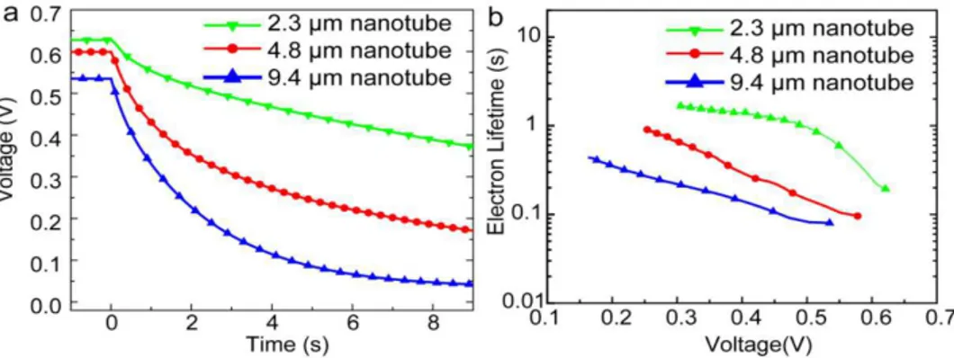
In 2014, Gao et al. [57] reported a perovskite-sensitized solar cell with a PCE of 5.52% using TiO2 NTs as the ETL for the first time. They used a two-step anodization process of Ti foil to form free standing TiO2NT membranes. By keeping the voltage constant and increasing the anodization time they could form free standing TiO2NTs of different lengths (2.3 µm, 4.8 µm, and 9.4 µm) which were
Nanomaterials 2017, 7, 95 9 of 27
transferred to a compact TiO2-coated FTO substrate. After casting MAPBI3on the TiO2NTs, they used an iodide-based liquid electrolyte to complete the solar cell. As shown in Figure7, the photovoltage in shorter NTs was found to decay more slowly compared to longer NTs, which indicated that longer NTs have a shorter electron lifetime and a higher charge recombination rate, resulting in a lower conversion efficiency. In a recent report [106], they ground down TiO2NTs to make discrete NTs and dissolved them in terpineol and ethanol. They subsequently spin coated this solution over a compact-TiO2film on a FTO substrate to obtain a NT network as the electron transport layer. They were able to achieve a short circuit current density of 24.8 mA·cm−2which is the highest recorded at present when using
MAPbI3as the active layer. The maximum PCE that they measured was 13.8% with a Vocand FF of 0.88 V and 0.63 respectively [106].
Nanomaterials 2017, 7, 95 9 of 26
make discrete NTs and dissolved them in terpineol and ethanol. They subsequently spin coated this solution over a compact-TiO2 film on a FTO substrate to obtain a NT network as the electron
transport layer. They were able to achieve a short circuit current density of 24.8 mAcm−2which is
the highest recorded at present when using MAPbI3 as the active layer. The maximum PCE that
they measured was 13.8% with a Vocand FF of 0.88 V and 0.63 respectively [106].
Figure 6. (a) IMPS and (b) IMVS plots of TiO2 nanoparticle and NT based DSSCs to calculate
transport time and recombination time respectively. Reprinted with permission from [20]. Copyright 2007 American Chemical Society.
Figure 7. (a) Open circuit voltage decay plots and (b) electron recombination lifetime vs. voltage plots of MAPbI3perovskite solar cells with different lengths of TiO2NTs as the ETL. Reprinted with
permission from Ref. [57], published by the Royal Society of Chemistry.
In 2014, Qin et al. directly formed TiO2NTs by anodizing a Ti-coated FTO substrate to obtain
TiO2NTs with lengths of 400–450 nm, pore diameters of 55–85 nm and wall thicknesses of 15–20 nm
[105]. The perovskite used was MAPbI3which was infiltrated into the titania nanotube ETL by the
solution-based sequential deposition method. Next, the hole transporting layer and gold contacts were deposited on top of the perovskite layer as shown in Figures 8c,d. Using these NTs as the ETL, they were able to achieve a PCE of 14.8%. In this report [105], perovskite could be effectively infiltrated into both the inside of the nanotubes as well as the inter-tubular spaces, allowing for effective charge transfer between the two materials. Furthermore, the use of a single-end open nanotube array ETL meant that the perovskite remained relatively sealed from external moisture, a problem that often occurs in TiO2,nanoparticle-based solar cells unless additional sealing is used.
Nevertheless, issues with the use of perovskite were found. Incomplete conversion of PbI2 to
CH3NH3PbI3 occurred, especially when compared to TiO2 nanoparticles, as shown in the XRD
spectrum in Figure 8e. The perovskite crystal size was also found to be smaller when deposited on
Figure 6.(a) IMPS and (b) IMVS plots of TiO2nanoparticle and NT based DSSCs to calculate transport time and recombination time respectively. Reprinted with permission from [20]. Copyright 2007 American Chemical Society.
Nanomaterials 2017, 7, 95 9 of 26
make discrete NTs and dissolved them in terpineol and ethanol. They subsequently spin coated this solution over a compact-TiO2 film on a FTO substrate to obtain a NT network as the electron
transport layer. They were able to achieve a short circuit current density of 24.8 mAcm−2 which is
the highest recorded at present when using MAPbI3 as the active layer. The maximum PCE that
they measured was 13.8% with a Vocand FF of 0.88 V and 0.63 respectively [106].
Figure 6. (a) IMPS and (b) IMVS plots of TiO2 nanoparticle and NT based DSSCs to calculate
transport time and recombination time respectively. Reprinted with permission from [20]. Copyright 2007 American Chemical Society.
Figure 7. (a) Open circuit voltage decay plots and (b) electron recombination lifetime vs. voltage plots of MAPbI3perovskite solar cells with different lengths of TiO2NTs as the ETL. Reprinted with
permission from Ref. [57], published by the Royal Society of Chemistry.
In 2014, Qin et al. directly formed TiO2NTs by anodizing a Ti-coated FTO substrate to obtain
TiO2NTs with lengths of 400–450 nm, pore diameters of 55–85 nm and wall thicknesses of 15–20 nm
[105]. The perovskite used was MAPbI3which was infiltrated into the titania nanotube ETL by the
solution-based sequential deposition method. Next, the hole transporting layer and gold contacts were deposited on top of the perovskite layer as shown in Figures 8c,d. Using these NTs as the ETL, they were able to achieve a PCE of 14.8%. In this report [105], perovskite could be effectively infiltrated into both the inside of the nanotubes as well as the inter-tubular spaces, allowing for effective charge transfer between the two materials. Furthermore, the use of a single-end open nanotube array ETL meant that the perovskite remained relatively sealed from external moisture, a problem that often occurs in TiO2,nanoparticle-based solar cells unless additional sealing is used.
Nevertheless, issues with the use of perovskite were found. Incomplete conversion of PbI2 to
CH3NH3PbI3 occurred, especially when compared to TiO2 nanoparticles, as shown in the XRD
spectrum in Figure 8e. The perovskite crystal size was also found to be smaller when deposited on
Figure 7. (a) Open circuit voltage decay plots and (b) electron recombination lifetime vs. voltage plots of MAPbI3perovskite solar cells with different lengths of TiO2NTs as the ETL. Reprinted with permission from Ref. [57], published by the Royal Society of Chemistry.
In 2014, Qin et al. directly formed TiO2 NTs by anodizing a Ti-coated FTO substrate to obtain TiO2 NTs with lengths of 400–450 nm, pore diameters of 55–85 nm and wall thicknesses of 15–20 nm [105]. The perovskite used was MAPbI3which was infiltrated into the titania nanotube ETL by the solution-based sequential deposition method. Next, the hole transporting layer and gold contacts were deposited on top of the perovskite layer as shown in Figure8c,d. Using these NTs as the ETL, they were able to achieve a PCE of 14.8%. In this report [105], perovskite could be effectively infiltrated into both the inside of the nanotubes as well as the inter-tubular spaces, allowing for effective charge transfer between the two materials. Furthermore, the use of a single-end open nanotube array ETL meant that the perovskite remained relatively sealed from external moisture, a problem that
often occurs in TiO2,nanoparticle-based solar cells unless additional sealing is used. Nevertheless, issues with the use of perovskite were found. Incomplete conversion of PbI2to CH3NH3PbI3occurred, especially when compared to TiO2nanoparticles, as shown in the XRD spectrum in Figure8e. The perovskite crystal size was also found to be smaller when deposited on nanotubes compared to nanoparticles, as shown in Figure 8a,b, this being an issue because a smaller crystal size results in a larger number of grain boundaries with concomitant increase in carrier trapping and charge recombination rate. Improved perovskite deposition methods and optimized nanotube dimensions could ameliorate these problems and lead to considerably higher efficiencies. The highest PCE of perovskite solar cells with TiO2NTs as the ETL at present is 15.2%, reported by Choi et al. [107]. They found that HPSCs using 40 nm-thick highly ordered single crystal-like TiO2nanopores obtained by anodizing sputtered Ti gave a better photovoltaic performance compared to HPSCs using spin-coated compact TiO2films because of the high contact area between anodic TiO2and perovskite as well as the superior electron transport properties of anodic TiO2NTs. Figure9shows the morphology of this one-dimensional TiO2layer.
Nanomaterials 2017, 7, 95 10 of 26
nanotubes compared to nanoparticles, as shown in Figures 8a and 8b, this being an issue because a smaller crystal size results in a larger number of grain boundaries with concomitant increase in carrier trapping and charge recombination rate. Improved perovskite deposition methods and optimized nanotube dimensions could ameliorate these problems and lead to considerably higher efficiencies. The highest PCE of perovskite solar cells with TiO2NTs as the ETL at present is 15.2%,
reported by Choi et al. [107]. They found that HPSCs using 40 nm-thick highly ordered single crystal-like TiO2 nanopores obtained by anodizing sputtered Ti gave a better photovoltaic
performance compared to HPSCs using spin-coated compact TiO2films because of the high contact
area between anodic TiO2and perovskite as well as the superior electron transport properties of
anodic TiO2NTs. Figure 9 shows the morphology of this one-dimensional TiO2layer.
Figure 8. Scanning electron microscopic (SEM) images of MAPbI3deposited on (a) TiO2nanotubes
and (b) TiO2nanoparticles, and cross-sectional images of a complete photovoltaic device using (c)
TiO2 nanotubes and (d) TiO2 nanoparticles; (e) X-ray diffraction (XRD) spectrum displaying the
incomplete conversion of PbI2 using TiO2 nanotubes. Reused with permission from Ref. [105].
Copyright 2015 Wiley and Sons.
Figure 8.Scanning electron microscopic (SEM) images of MAPbI3deposited on (a) TiO2nanotubes and (b) TiO2nanoparticles, and cross-sectional images of a complete photovoltaic device using (c) TiO2 nanotubes and (d) TiO2nanoparticles; (e) X-ray diffraction (XRD) spectrum displaying the incomplete conversion of PbI2using TiO2nanotubes. Reused with permission from Ref. [105]. Copyright 2015 Wiley and Sons.
Nanomaterials 2017, 7, 95 11 of 27
Nanomaterials 2017, 7, 95 11 of 26
Figure 9. Top SEM image of (a) bare FTO (b) Ti sputtered on FTO (c) anodized TiO2 and (d)
cross-sectional SEM image of anodized TiO2. Reprinted with permission from Ref. [107]. Copyright
2016 American Chemical Society.
Wang et al. demonstrated backside illuminated flexible perovskite solar cells by using anodized TiO2NTs on Ti foil as the ETL with a PCE of 8.31% which was the highest reported PCE
of flexible perovskite solar cell at that time [108]. A major problem limiting PCEs with backside illuminated solar cells is the strong absorption of ultraviolet and violet photons by the HTL, thus leading to low external quantum efficiencies for wavelengths in the range 359–425 nm [108]. Similarly, Salazar et al. demonstrated HTL-free perovskite solar cells with anodized TiO2NTs on
FTO as the ETL with a PCE of 5% [109].
Table 1. Summary of solar cell performance reported to date for one-dimensional TiO2ETLs.
Year Device
S
tructure VOC(V) (mA cmJSC −2) FF PCE (%) Ref.
2013 FTO|TiO2BL|TiO2 NR|MAPbI3|Spiro|Au 0.82 10.1 0.59 4.87 [110] 2013 FTO|TiO2BL|TiO2 NR|MAPbI3|Spiro|Au 0.96 15.6 0.63 9.40 [111] 2014 FTO|TiO2BL|TiO2 NR|MAPbI3|Spiro|Au 0.77 22.3 0.68 11.7 [112]
2014 FTO|TIO2BL|TIO2NT| MAPbI3|Spiro 0.63 17.9 0.58 6.52 [57]
2014 FTO|TiO2BL|Nb-TiO2NR|MAPbIxBr3-x
|Spiro|Au 0.87 16.5 0.52 7.50 [113]
2014 FTO|TiO2BL|Sn-TiO2
NR|MAPbI3|Spiro|Ag 0.74 14.9 0.52 6.31 [114]
2015 FTO|TiO2BL|TiO|Spiro|Au2NR/Layer|MAPbI3 0.95 19.8 0.72 13.5 [115,116]
2015 FTO|TiO2NT|MAPbI3|Spiro|Au 1.07 22.6 0.64 14.8 [105]
2015 FTO|TiO2BL|TIO2NT|MAPbI3|Au 0.67 19.6 0.37 5.00 [109]
2015 Ti|TiO2NT| MAPbI3|CNT Film|Spiro 0.99 14.4 0.68 8.31 [108]
Figure 9. Top SEM image of (a) bare FTO (b) Ti sputtered on FTO (c) anodized TiO2 and (d) cross-sectional SEM image of anodized TiO2. Reprinted with permission from Ref. [107]. Copyright 2016 American Chemical Society.
Wang et al. demonstrated backside illuminated flexible perovskite solar cells by using anodized TiO2NTs on Ti foil as the ETL with a PCE of 8.31% which was the highest reported PCE of flexible perovskite solar cell at that time [108]. A major problem limiting PCEs with backside illuminated solar cells is the strong absorption of ultraviolet and violet photons by the HTL, thus leading to low external quantum efficiencies for wavelengths in the range 359–425 nm [108]. Similarly, Salazar et al. demonstrated HTL-free perovskite solar cells with anodized TiO2NTs on FTO as the ETL with a PCE of 5% [109].
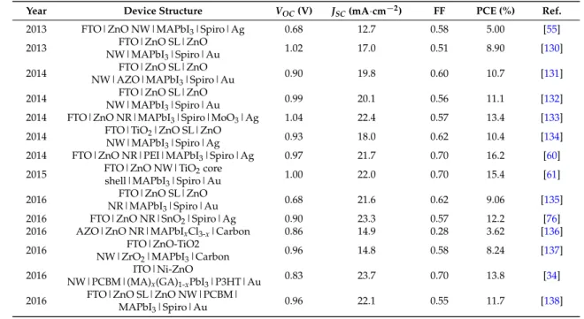
Table 1.Summary of solar cell performance reported to date for one-dimensional TiO2ETLs. Year Device Structure VOC(V) JSC(mA·cm−2) FF PCE (%) Ref.
2013 FTO|TiO2BL|TiO2 NR|MAPbI3|Spiro|Au 0.82 10.1 0.59 4.87 [110] 2013 FTO|TiO2BL|TiO2 NR|MAPbI3|Spiro|Au 0.96 15.6 0.63 9.40 [111] 2014 FTO|TiO2BL|TiO2 NR|MAPbI3|Spiro|Au 0.77 22.3 0.68 11.7 [112] 2014 FTO|TIO2BL|TIO2NT| MAPbI3|Spiro 0.63 17.9 0.58 6.52 [57] 2014 FTO|TiO2BL|Nb-TiO2 NR|MAPbIxBr3-x|Spiro|Au 0.87 16.5 0.52 7.50 [113] 2014 FTO|TiO2BL|Sn-TiO2 NR|MAPbI3|Spiro|Ag 0.74 14.9 0.52 6.31 [114] 2015 FTO|TiO2BL|TiO2 NR/Layer|MAPbI3|Spiro|Au 0.95 19.8 0.72 13.5 [115,116]
2015 FTO|TiO2NT|MAPbI3|Spiro|Au 1.07 22.6 0.64 14.8 [105]
2015 FTO|TiO2BL|TIO2NT|MAPbI3|Au 0.67 19.6 0.37 5.00 [109]
2015 Ti|TiO2NT|MAPbI3|CNT
Film|Spiro 0.99 14.4 0.68 8.31 [108]
2016 FTO|TiO2BL|TiO2
NR|MAPbI3|Spiro|Au 1.04 22.9 0.76 18.2 [116]
2016 FTO|TiO2NT|MAPbI3-xAcx|Ag 1.06 20.5 0.7 15.2 [107]
2017 FTO|TiO2BL|TiO2NT
6.2. TiO2Nanorod Arrays
TiO2 nanorods (NRs) are another popular configuration for ETLs in perovskite solar cells (summarized in Table1). TiO2nanorods are another popular one-dimensional nanostructure that has attracted tremendous interest as ETLs in perovskite solar cells (summarized in Table1). Among the various methods to grow TiO2NRs—such as sol–gel processes [117], chemical vapor deposition [118–120], vapor-liquid-solid growth [121], and pulsed laser deposition [122]—hydro/solvothermal synthesis is the simplest method to obtain high quality TiO2NRs [123]. Hydrothermal synthesis refers to a heterogeneous reaction occurring under high pressure and temperature in the presence of aqueous solvents to dissolve and subsequently recrystallize the material that under ordinary conditions would be insoluble [112,124]. Solvothermal methods are similar to hydro-thermal methods except the solvent used is non-aqueous [125]. Most highly efficient perovskite solar cells have the TiO2nanowire ETLs grown by hydrothermal synthesis, which has the added advantage of being directly synthesizable on rutile-phase FTO-coated (amorphous) glass substrates [125]. Unlike the anodic TiO2nanotubes, TiO2nanorods fabricated by the hydrothermal process are composed of the rutile phase of TiO2[123], which exhibits inferior electronic properties in comparison to the anatase phase of TiO2. Even though anatase nanorod arrays have been used in dye-sensitized solar cells, their synthesis is less facile compared to rutile nanorod arrays which may be why their use in HPSCs has not been prominent. The length and diameter of the solvothermally grown rutile nanorod arrays are controlled by synthesis conditions, such as temperature, pressure, precursor solution composition, pH, and reaction time. Hydro/solvothermal synthesis provides flexibility in being able to tune the dimension and aspect ratio of TiO2NRs just by changing the growth time and concentration of precursor. Qui et al. was first to use TiO2nanorods as an ETL with perovskite as the light absorber [110]. Using a thin layer of MAPbBr3on 1.5 µm tall nanorods, they reported a PCE of 4.87% [110]. This report triggered new research on application of TiO2nanorods as an electron transport layer for perovskite solar cells. Park et al. [111] compared performance of longer and shorter TiO2, nanorods. Though they could not find any considerable difference in recombination resistance between longer and shorter nanorods, they concluded that shorter nanorods could provide better infiltration of perovskite. By using MAPbI3 as a light absorber, they were able to achieve a PCE of about 9.4% [111]. In 2014, Jiang et al. [112] fabricated a perovskite solar cell using 900 nm-long TiO2 nanorods as the ETL and achieved an efficiency of 11.7%, a record for TiO2nanorods at that time. The higher efficiency was attributed to wide-open voids between the nanorods into which perovskite was able to effectively infiltrate [112]. In 2012, the same group reported on the faster electron transport capabilities of TiO2 nanorods compared to mesoscopic TiO2[21]. Subsequently, several devices using this structure were reported, having a PCE lower than 15% [56,126,127]. Subsequently, Hong et al. were able to demonstrate in 2015 a TiO2-nanorod based perovskite solar cell with an efficiency of 13.5%, achieved by passivating the surface of the nanorods with a thin layers of TiO2in an attempt to limit and grain boundaries surface traps [115]. Most recently, in 2016, Li et al. were able to achieve record efficiencies of 18.22% [116], shown in Figure10. In this work, the diameter and lengths of the nanorods used were around 2–40 nm and 180 nm respectively and were synthesized from a precursor containing 2-ethyl-butyric acid. They were able to achieve excellent perovskite deposition, and in so doing, ensured no contact between the TiO2and the hole transporting layer. Furthermore, they utilized a UV-ozone cleaning process to eliminate organic residues on the nanorod surface, strengthening the contact between perovskite and TiO2and thus decreasing surface traps and increasing the efficiency.
Nanomaterials 2017, 7, 95 13 of 27
Nanomaterials 2017, 7, 95 13 of 26
Figure 10. (a) Top-view SEM image of TiO2 nanowires; (b) Cross-sectional SEM image of TiO2
nanowires; (c) Cross-sectional SEM image of perovskite solar cell fabricated using a TiO2nanowire
array as the ETL; and (d) J–V curve of the best performing perovskite solar cell with TiO2nanowire
array ETL. Adapted with permission from Ref. [116]. Copyright 2016 American Chemical Society.
6.3. ZnO Nanorod Arrays
ZnO is an n-type semiconductor with band gap of 3.37 eV and a higher electron mobility than TiO2[128,129]. This results in less recombination loss in ZnO compared to TiO2, which makes ZnO
superior in balancing the charge transport in perovskite. The reported photovoltaic performance of perovskite solar cells fabricated using ZnO NRs as the ETL is summarized in Table 2.
Table 2. Summary of solar cell performance reported to date for one dimensional ZnO ETLs.
Year Device structure VOC
(V)
JSC
(mA cm−2) FF
PCE
(%) Ref.
2013 FTO|ZnO NW|MAPbI3|Spiro|Ag 0.68 12.7 0.58 5.00 [55]
2013 FTO|ZnO SL|ZnO NW|MAPbI3|Spiro|Au 1.02 17.0 0.51 8.90 [130]
2014 NW|AZO|MAPbIFTO|ZnO SL|ZnO
3|Spiro|Au 0.90 19.8 0.60 10.7 [131]
2014 FTO|ZnO SL|ZnO NW|MAPbI3|Spiro|Au 0.99 20.1 0.56 11.1 [132]
2014 FTO|ZnO NR|MAPbI3|Spiro|MoO3|Ag 1.04 22.4 0.57 13.4 [133]
2014 FTO|TiO2|ZnO SL|ZnO
NW|MAPbI3|Spiro|Ag 0.93 18.0 0.62 10.4 [134]
2014 FTO|ZnO NR|PEI|MAPbI3|Spiro|Ag 0.97 21.7 0.70 16.2 [60]
2015 FTO|ZnO NW|TiO2core
shell|MAPbI3|Spiro|Au 1.00 22.0 0.70 15.4 [61]
2016 FTO|ZnO SL|ZnO NR|MAPbI3|Spiro|Au 0.68 21.6 0.62 9.06 [135]
2016 FTO|ZnO NR|SnO2|Spiro|Ag 0.90 23.3 0.57 12.2 [76]
Figure 10. (a) Top-view SEM image of TiO2 nanowires; (b) Cross-sectional SEM image of TiO2 nanowires; (c) Cross-sectional SEM image of perovskite solar cell fabricated using a TiO2nanowire array as the ETL; and (d) J–V curve of the best performing perovskite solar cell with TiO2nanowire array ETL. Adapted with permission from Ref. [116]. Copyright 2016 American Chemical Society. 6.3. ZnO Nanorod Arrays
ZnO is an n-type semiconductor with band gap of 3.37 eV and a higher electron mobility than TiO2[128,129]. This results in less recombination loss in ZnO compared to TiO2, which makes ZnO superior in balancing the charge transport in perovskite. The reported photovoltaic performance of perovskite solar cells fabricated using ZnO NRs as the ETL is summarized in Table2.
Table 2.Summary of solar cell performance reported to date for one dimensional ZnO ETLs.
Year Device Structure VOC(V) JSC(mA·cm−2) FF PCE (%) Ref.
2013 FTO|ZnO NW|MAPbI3|Spiro|Ag 0.68 12.7 0.58 5.00 [55]
2013 FTO|ZnO SL|ZnO NW|MAPbI3|Spiro|Au 1.02 17.0 0.51 8.90 [130] 2014 FTO|ZnO SL|ZnO NW|AZO|MAPbI3|Spiro|Au 0.90 19.8 0.60 10.7 [131] 2014 FTO|ZnO SL|ZnO NW|MAPbI3|Spiro|Au 0.99 20.1 0.56 11.1 [132]
2014 FTO|ZnO NR|MAPbI3|Spiro|MoO3|Ag 1.04 22.4 0.57 13.4 [133]
2014 FTO|TiO2|ZnO SL|ZnO
NW|MAPbI3|Spiro|Ag 0.93 18.0 0.62 10.4 [134]
2014 FTO|ZnO NR|PEI|MAPbI3|Spiro|Ag 0.97 21.7 0.70 16.2 [60]
2015 FTO|ZnO NW|TiO2core
shell|MAPbI3|Spiro|Au 1.00 22.0 0.70 15.4 [61]
2016 FTO|ZnO SL|ZnO
NR|MAPbI3|Spiro|Au 0.68 21.6 0.62 9.06 [135]
2016 FTO|ZnO NR|SnO2|Spiro|Ag 0.90 23.3 0.57 12.2 [76]
2016 AZO|ZnO NR|MAPbIxCl3-x|Carbon 0.86 14.9 0.28 3.62 [136]
2016 FTO|ZnO-TiO2
NW|ZrO2|MAPbI3|Carbon 0.96 14.8 0.58 8.24 [137]
2016 ITO|Ni-ZnO
NW|PCBM|(MA)x(GA)1-xPbI3|P3HT|Au 0.83 23.7 0.70 13.8 [34]
2016 FTO|ZnO SL|ZnO NW|PCBM|
Table 3. Summary of reported device performances from solar cells incorporating ETLs containing composites and unusual morphologies.
Year Device Structure VOC(V) JSC(mA·cm−2) FF PCE (%) Ref.
2016 FTO|ZnO-TiO2
NW|ZrO2|MAPbI3|Carbon 0.96 14.8 0.58 8.24 [137]
2016 ITO|Ni-ZnO
NW|PCBM|(MA)x(GA)1-xPbI3|P3HT|Au 0.83 23.7 0.70 13.8 [34]
2015 FTO|ZnO NW|TiO2core
shell|MAPbI3|Spiro|Au 1.00 22.0 0.70 15.4 [61]
2014 FTO|TiO2|ZnO SL|ZnO
NW|MAPbI3|Spiro|Ag 0.93 18.0 0.62 10.4 [134] 2014 FTO|TiO2BL/SL|Nb-TiO2 NR|MAPbIxBr1-x|Spiro|Au 0.87 16.5 0.52 7.50 [113] 2014 FTO|TiO2SL|Sn-TiO2 NR|MAPbI3|Spiro|Ag 0.74 14.9 0.52 6.31 [114] 2015 FTO|TiO2BL|TiO2 NR/Layer|MAPbI3|Spiro|Au 0.95 19.8 0.72 13.5 [115] 2015 FTO|WO3BL|WO3
NR|TiO2|MAPbI3|Spiro|Ag 0.86 15.00 0.70 9.10 [38]
Hydrothermal growth of ZnO NRs is most commonly used compared to other methodologies like the galvanic cell-based methods [136], electrochemical methods [76,139,140], and magnetron sputtering [133] because of its flexibility in morphology tuning by adjusting conditions like growth time, growth temperature, precursor concentration, and addition of capping agents in the precursor [60,62,141]. In the hydrothermal growth of ZnO NRs, a thin seed layer of ZnO is deposited over the substrate by spin coating, sputtering, or chemical vapor deposition. Seeding of ZnO lowers the thermodynamic barrier by providing nucleation sites and also helps to improve the aspect ratio of the obtained rods [142]. The substrate with the seed layer is then kept in growth solution for the desired time. The growth solution is an aqueous solution of an alkaline reagent like sodium hydroxide or hexamethylenetetramine (HMTA) and a Zn2+salt like Zn(NO)3or ZnCl2. After synthesis, the ZnO NRs are washed and dried. The diameter of such NRs can be modified by changing the precursor solution while their length can be tuned by varying growth time [132]. Son et al. compared the performance of ZnO NRs and rutile TiO2NRs as ETLs and found that ZnO NRs have a lower recombination rate compared to rutile TiO2NRs, shown in Figure11[132].
Nanomaterials 2017, 7, 95 14 of 26
2016 AZO|ZnO NR|MAPbIxCl3-x|Carbon 0.86 14.9 0.28 3.62 [136]
2016 FTO|ZnO-TiO2 NW|ZrO2|MAPbI3|Carbon 0.96 14.8 0.58 8.24 [137]
2016 NW|PCBM|(MA)ITO|Ni-ZnO
x(GA)1-xPbI3|P3HT|Au 0.83 23.7 0.70 13.8 [34]
2016 FTO|ZnO SL|ZnO NW|PCBM|
MAPbI3|Spiro|Au 0.96 22.1 0.55 11.7 [138]
Hydrothermal growth of ZnO NRs is most commonly used compared to other methodologies like the galvanic cell-based methods [136], electrochemical methods [76,139,140], and magnetron sputtering [133] because of its flexibility in morphology tuning by adjusting conditions like growth time, growth temperature, precursor concentration, and addition of capping agents in the precursor [60,62,141]. In the hydrothermal growth of ZnO NRs, a thin seed layer of ZnO is deposited over the substrate by spin coating, sputtering, or chemical vapor deposition. Seeding of ZnO lowers the thermodynamic barrier by providing nucleation sites and also helps to improve the aspect ratio of the obtained rods [142]. The substrate with the seed layer is then kept in growth solution for the desired time. The growth solution is an aqueous solution of an alkaline reagent like sodium hydroxide or hexamethylenetetramine (HMTA) and a Zn2+ salt like Zn(NO)
3 or ZnCl2. After
synthesis, the ZnO NRs are washed and dried. The diameter of such NRs can be modified by changing the precursor solution while their length can be tuned by varying growth time [132]. Son et al. compared the performance of ZnO NRs and rutile TiO2NRs as ETLs and found that ZnO NRs
have a lower recombination rate compared to rutile TiO2NRs, shown in Figure 11 [132].
Figure 11. Comparison between time constant for charge recombination (τR) as a function of light
intensity, represented by photocurrent density, for ZnO and TiO2NRs. Adapted with permission
from Ref. [132]. Copyright 2014 American Chemical Society.
In 2013, Bi et al. [55] compared the performance of ZnO NR ETLs with mesoporous TiO2ETL
in MAPbI3 solar cells with spiro-MeOTAD as the HTM. Cross-sectional FESEM images showed
excellent infiltration of the ZnO NR ETL by the solution processed MAPbI3. The photocurrent
density increased from 8.9 mA·cm−2to 12.7 mA·cm−2as the length of ZnO NRs was increased from
400 nm to 1000 nm due to increased harvesting of photons by a thicker perovskite coating of the NRs. Bi et al. [55] found the electron transport time of ZnO NRs to be faster than that in mesoporous TiO2ETLs with the same thickness, but also observed that recombination in ZnO NRs
due to back-electron transfer was higher than that for TiO2ETLs. This caused a reduction in open
circuit voltage, particularly with increasing ZnO NR length; hence ZnO-based solar cells exhibited a lower overall efficiency compared to mesoporous TiO2-based solar cells [55]. Further increase in the
length of ZnO NRs caused a reduction in electron life time (τe) and an increase in electron transport
Figure 11. Comparison between time constant for charge recombination (τR) as a function of light intensity, represented by photocurrent density, for ZnO and TiO2NRs. Adapted with permission from Ref. [132]. Copyright 2014 American Chemical Society.


![Figure 4. Time-resolved photoluminescence (along with stretched exponential fits) of MAPbI 3 using the electron quencher [6,6]-phenyl-C 61 -butyric acid methyl ester (PCBM) shown as blue trianges or using the hole quencher layer Spiro-MeOTAD, shown as red](https://thumb-eu.123doks.com/thumbv2/123doknet/14066470.462042/7.892.245.650.410.714/resolved-photoluminescence-stretched-exponential-electron-quencher-trianges-quencher.webp)