HAL Id: hal-02514766
https://hal.archives-ouvertes.fr/hal-02514766
Submitted on 22 Mar 2020
HAL is a multi-disciplinary open access
archive for the deposit and dissemination of
sci-entific research documents, whether they are
pub-lished or not. The documents may come from
teaching and research institutions in France or
abroad, or from public or private research centers.
L’archive ouverte pluridisciplinaire HAL, est
destinée au dépôt et à la diffusion de documents
scientifiques de niveau recherche, publiés ou non,
émanant des établissements d’enseignement et de
recherche français ou étrangers, des laboratoires
publics ou privés.
A. Wiesner, R. Diez, D. Florez, Hubert Piquet
To cite this version:
A. Wiesner, R. Diez, D. Florez, Hubert Piquet. DESIGN OF A POWER SUPPLY CAPABLE OF
DRIVING A DIVERSE SET OF DBD EXCILAMPS. ELECTRIMACS 2017, Jul 2017, Toulouse,
France. �hal-02514766�
D
ESIGN OF A
P
OWER
S
UPPLY
C
APABLE OF
D
RIVING A
D
IVERSE
S
ET
OF
DBD
E
XCILAMPS
A. Wiesner
1,2, R. Diez
1, D. Florez
1,3, H. Piquet
21. Pontificia Universidad Javeriana, Carrera 7 No. 40-62, 110231 Bogotá, Colombia
2. LAPLACE, Université de Toulouse, CNRS, INPT, UPS, 2 rue Charles Camichel, 31071 Toulouse, France 3. Universidad Sergio Arboleda, Calle 74 No. 14-14, 110221 Bogotá, Colombia
E-mail: wiesner@laplace.univ-tlse.fr
Abstract – In this work the procedure to design a power supply capable of supplying nineteen different exciplex Dielectric Barrier Discharge (DBD) UV lamps, is shown. This power supply is studied with the aim to study the impact of the DBD lamp geometrical characteristics over system’s performances (UV emission, efficiency). The pulsed power supply can control and adjust three electric parameters: frequency, amplitude and duration of the current pulses. For this reason, a wide operating range is needed and the choice of the elements for the power supply is a challenge. Modeling of the lamps is used to define the most interesting operating points to be explored and also for the selection of the devices ratings and the parameters of the supply (semiconductors, control, transformer).
Keywords – DBD, exciplex, power converter, current mode.
1. I
NTRODUCTIONDielectric Barrier Discharge (DBD) UV lamps are environmentally friendly (mercury free) UV sources with various applications: disinfection, microelectronics, surface treatments, health. The practical usefulness and applicability of currently available DBD excilamps has been demonstrated
[1]; today, studies oriented toward their
performance improvement are in development. This can be achieved by means of the reactor design optimization (geometry, filling mixture, pressure and materials) [2], [3] and also by choosing the most performing electrical operating conditions [4], [5].
The impact of the electrical operating point (OP) over the DBD excilamps performance has been already reported by different teams [1], [7] and [6]. However, because a DBD excilamp design cannot be easily adjusted [8] and constructed, most of these studies are developed for a fixed lamp design and the impact of the DBD lamp geometry over the lamp performance has not been widely reported.
With the aim to provide deeper insight and experimental evidence about the impact of the geometry of the DBD reactor, a set of nineteen diverse DBD exciplex UV lamps of coaxial type, has been built, as shows the Fig. 1: T is the dielectric thicknesses, a is the internal radius, b is the external radius and l is the length of the lamp. Each one of the 19 bulbs present a different parameter set {T, a, b, l}; these lamps were designed and manufactured, differing among them in their dielectric thicknesses and clearances (gas gap), and filled with the same gas mixture.
The proposed study consists on supplying the different excilamps at different controlled electrical operating points, comparing the lamp performances in terms of the obtained UV power and of the system’s electrical power to UV power efficiency; for each experiment, the parameters of the electrical model of the bulb are identified.
From previous works a significant impact of the lamp operating point over the lamp performance has been evidenced. Particularly, the methodology proposed in [5] makes use of a square-shape current waveform for the parametric study of DBDs. By
means of the iDBD current waveform, the lamp
power can be controlled with three degrees of freedom: duty cycle (D), current intensity (J) and frequency (f) of the current pulses, as show in Fig. 3.
Fig. 3. DBD current and voltage waveforms using a square-shape current source.
The topology of the power supply consists in a constant current source connected in cascade to a full-bridge inverter [5], as shown on Fig. 2. A step-up transformer is used to connect the bulb to the
current inverter. The dimensioning and
implementation of this converter for the current study is a challenge due to the wide range of operating conditions implied by the set of 19 lamps. According to the dimensions of the bulbs the power range of this supply from has been chosen from 0 to 500W.
This design process is presented as follows: first, the electrical model of each lamp is theoretically obtained as a basis for the converter design. Then, using these models and taking into account the different characteristics of the 19 bulbs, the operating range of interest, concerning the properties of the current pulses, is determined. Finally, the converter design is presented, pointing out the challenges of supplying such a different set of loads and at this level of power (up to 500W).
2. DBD
LAMPS UNDER STUDYThe nineteen coaxial DBD lamps, used for this work, present the configuration shown in Fig. 1 and have different geometrical parameters that are categorized as:
External diameter: with two different values,25mm and 45mm.
Internal diameter: six different values varying
from 5mmto 30mm in steps of 5mm.
Thickness of the dielectric barriers: three
different values, 1, 1.5 and 2mm. The inner and outer barrier thickness is the same for each lamp. All the lamps have a length (l) of 600mm. The gas mixture used to fill the lamp bulbs is XeCl, producing a radiation wavelength at 308nm. In order to design a power supply capable of driving all the lamps under study, initially, the electrical magnitudes are calculated using the simplified electrical model of the DBD developed in [9], as shown in Fig. 4.
Fig. 4. DBD electrical model.
Cd is the dielectric series equivalent capacitance, Cg
the gas equivalent capacitance and Vth the gas
breakdown voltage. The lamp model parameters are estimated using the cylindrical capacitor equation
(1) and (2), for the values of Cg and Cd and using
the Paschen’s law (3) for the breakdown voltage Vth. 𝐶𝑔= 2𝜋∙𝜀𝑔∙𝑙 𝐼𝑛 (𝑏𝑎) ≈ 𝑦 𝑙 𝐼𝑛 (𝑏𝑎) (1) Fig. 2. DBD power supply.
𝐶𝑑= 2𝜋∙𝜀𝑑∙𝑙∙ 1 𝑙𝑛 (𝑇2+ 𝑎∙𝑇 + 𝑏𝑎∙𝑏∙𝑇 + 𝑎∙𝑏) 𝐶𝑑≈ 𝑧∙𝑙∙ 1 𝑙𝑛 (𝑇2+ 𝑎∙𝑇 + 𝑏𝑎∙𝑏∙𝑇 + 𝑎∙𝑏) (2) 𝑉𝑡ℎ= 𝐶 ∙ 𝑝𝑔𝑎𝑠∙ 𝑑 𝐼𝑛 (𝐴 ∙ 𝑝𝑔𝑎𝑠∙ 𝑑 𝐼𝑛 (1 +1𝛾) ) ≈ 𝑋 𝑑 𝐼𝑛(𝑑) (3)
a, b, l and T are the geometrical parameters of the lamp; A is a constant which depends on the electron kinetic temperature, C is related to A and to the
effective ionization potential V * (C=A V*), 𝑝
𝑔𝑎𝑠 is
the pressure, d is the distance between dielectrics, 𝛾 is the electron emission coefficient [10].
In these three equations, the
𝑦,
𝑋 and𝑧
terms areconstants, which values are derived from
measurements achieved on a bulb with the same material for walls, gas mixture and pressure [8]. With the geometry known for each lamp, the values for the components of electrical model are calculated, obtaining the range in Table 1.
Table 1: Electrical values
Range Dielectric capacitance (Cd) 34pF - 200nF
Gas capacitance (Cg) 96pF - 84nF Threshold voltage (Vth) 375V - 2400V
3. O
PERATING POINTS RANGEIn order to design the power supply, a maximum power value of 500W is chosen. Once the electrical model for each lamp is obtained, it is possible to find out the values of the J amplitude of the lamp
current (iDBD) and the peak voltage for those lamps,
thanks to equations (3) and (4), deduced from work detailed in [5]. 𝐽 = 𝑃 𝐷 ∙ 𝑉𝑡ℎ + 𝑓4 ∙ 𝐶𝑔∙ 𝑉𝑡ℎ 𝐷 (4) 𝑉̂𝐷𝐵𝐷 = 𝑉𝑡ℎ+ 𝐽 ∙ 𝐷 4 ∙ 𝑓 ∙ 𝐶𝑑 (5)
P is the desired average electric poweron the DBD; D, J, f are the three degrees of freedom of the iDBD
current shape, controlled thanks to the current inverter (f, D) and the current source (J*N, N being
the turn ratio of the transformer). Cd, Cg, 𝑉𝑡ℎ are the
DBD electrical model parameters.
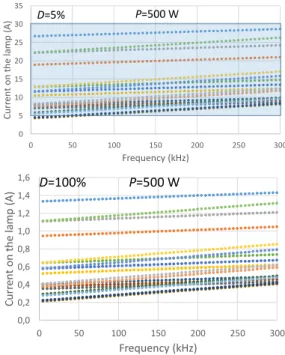
Fig. 5 presents the current pulse amplitude J, obtained from eq(4), versus the f frequency for two different duty cycles (D=5% and D=100%) and for the maximum requested power (P=500W). As expected, the lower the duty cycle, the higher the J current amplitude. One can observe that the required power is obtained, for D=100%, with a relatively low J value (to remember, that this value will define the operating conditions of the current inverter and of the current source; these converters will have to control a J*N current, N being the turn ratio of the transformer). In order to avoid oversizing of the current converters, the maximum J=1.6A value has been selected. As a matter of fact, almost all the points associated with the D=5% duty ratio will be unreachable (shadowed area). For the shadowed operating points, the specific power (power per unit of bulb’s length), which is unreachable using the full length of the bulb, will be attained thanks to an outer metallic electrode of reduced length.
Combining eq (4) in eq(5), we obtain the following equation (6), where it appears that the lamp peak
voltage (𝑉̂𝐷𝐵𝐷) does not explicitly depends on the
duty cycle D. 𝑉̂𝐷𝐵𝐷= 𝑉𝑡ℎ(1 + 𝐶𝑔 𝐶𝑑 ) + 𝑃 𝑓 ∙ 4 ∙ 𝐶𝑑∙ 𝑉𝑡ℎ (6)
For the same P=500W power level, Fig. 6 presents
the lamp peak voltage (𝑉̂𝐷𝐵𝐷) versus frequency, for
the 19 lamps.
Fig. 5. Current in the 19 lamps as a function of the frequency. Cases for duty cycle of 5% (top) and 100% (bottom). 0 5 10 15 20 25 30 35 0 50 100 150 200 250 300 C urr en t on t he la mp (A ) Frequency (kHz) D=5% P=500 W 0,0 0,2 0,4 0,6 0,8 1,0 1,2 1,4 1,6 0 50 100 150 200 250 300 C urr ent on t he la mp (A ) Frequency (kHz) D=100% P=500 W
This figure shows that the requested lamp voltage in low frequencies is very high. To avoid oversizing of the step-up transformer, the minimum operating frequency has been limited to 30kHz. The maximum operating frequency has been set to 200kHz considering implementation aspects, as the speed of semiconductor devices and the limitation of magnetic materials.
To conclude this section, we summarize below the
operating range of the parameters of the iDBD pulses:
0 < J < 1.6A
5% < D < 100%
30kHz < f < 200kHz
4. C
ONVERTER DESIGNAfter finding the operating range for the 3 degrees of freedom to make the DBD characterizations, the system design is now achieved.
4.1 Inverter switch selection
The selection of the inverter switches is performed under the assumption that the power can be delivered to the lamp, independently of the turn ratio of the transformer that will be chosen later. For that purpose, the product of voltage and current in each lamp is obtained for the most demanding
case, multiplying Fig. 5 (D=100%) and Fig. 6,
resulting in the decaying curve shown in Fig. 7 for a given lamp.
The obtained curve is compared to the product of the blocking voltage and the current rating of the candidate switches for the converter (flat lines in
intersection between the lamp and switch curves are the ones that cannot be attained by the switch, regardless of the transformer ratio to be chosen. The switch is chosen using a compromise between its price and the number of reachable OP. Fig. 6 is useful to determine the value of the minimum operating frequency for the selected switch.
4.2. Transformer
Once the switches have been chosen, the interesting OPs from Fig. 7 are tested for different transformer’s turn ratios (N). The points to be discarded are the ones where the peak voltage or the current in the lamp (seen in the primary side of the transformer) exceeds the ratings of the switch. The points with power losses in the switches greater than 30W are also removed, due to thermal limitation for the available cooling system (classical dissipators).
Fig. 8 shows the result of this analysis and the transformation ratio is selected maximizing the number of reachable points, but also assuring a wide frequency range. In this case a turn ratio of 10 is selected.
4.3. Current source
To avoid the influence of the iDBD current ripple on
the DBD performance, the frequency of the current source which supplies the current inverter should be much higher than the maximum frequency of the
latter: the fmax=200kHz selected value makes it
impossible to satisfy this condition. For this reason, parallelized current choppers, with an interleaved configuration allow the reduction on the magnetic cores and increase the apparent frequency of the delivered current.
Fig. 6. Lamp peak voltage as a function of the frequency. 0 5 10 15 20 25 30 35 40 45 50 0 50 100 150 200 250 300 P eak V ol ta ge (k V ) Frequency (kHz) P=500 W
Fig. 7. Selection of the switches via the V I product.
0 5 10 15 20 25 30 35 20 60 100 140 180 220 260 300 P roduct V *I ( kV A ) Frequency (kHz) C2M0040120D C2M0080120D C3M0065090D C3M0065090J C3M0120090D C2M0160120D C2M0280120D C3M0280090D C2M1000170J C2M1000170D
Fig. 8. Operating points attained vs. the frequency for different turns ratio of the transformer.
0 5 10 15 20 25 0 20 40 60 80 100 120 140 160 180 200 220 240 260 280 300 N um be r of O pe ra ti ng P oi nt s Frequency (kHz) N:6 N:8 N:10 N:12 N:14
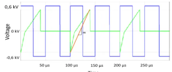
Fig. 9. output voltage of the chopper vch and input voltage of
m 0,6 kV 0 kV -0,6 kV Time 50 μs 100 μs 150 μs 200 μs Volt age 250 μs
Therefore, the maximum frequency of the current sources is defined by the speed of semiconductor devices, switching losses and the limitation of magnetic materials. Thus the maximum frequency on the inverter and the maximum frequency on each current source are similar as shown in Fig. 10, This
figure plots the output voltage of the chopper vch
and the input voltage of the current inverter vB.
Finally, the L inductor which controls the current ripple at the input of the current inverter is defined. In that scope, we use eq. (10). The current ripple on the L inductor is defined by:
(7)
(8)
Assuming the approximation of the shape of the vB
voltage, highlighted with the red slope (m) in Fig. 10, the current ripple is defined by:
𝑚 ≈2 ∙ 𝑉𝑝∙𝑓 𝑁 ∙ 𝐷 (9) ∆𝑖𝐿= 𝐷𝑐ℎ 𝐿 ∙ 𝑓𝑐ℎ (𝑉𝑖𝑛− 𝑣𝐵− 𝑉𝑝∙ 𝑓 ∙ 𝐷𝑐ℎ 𝑁 ∙ 𝑓𝑐ℎ∙ 𝐷 ) (10)
vB is a variable voltage that varies between –Vp and
Vp as shown in Fig. 9, N is the turns ratio on the
transformer, f and D are the frequency and duty
cycle on the current inverter and fch and Dch are the
frequency and duty cycle on the current source. Note that this converter differs from conventional
DC-DC converters, because 𝑣𝐵 changes and it is
dependent on the inverter frequency. This fact implies a high inductance value to maintain a low current ripple.
4.4. Working range
Once defined the different devices of the system, it is important to finally find out the actual possible OP for each lamp. In this scope, a cloud of accessible operating points is plotted: for each lamp, varying f in steps of 5kHz, D in steps of 5% and J in steps of 0.2A.
In Fig. 10, we observe for one specific lamp that the three degrees of freedom form a cube with all possible OP: within this cube, the green cells are the most interesting OP for the experiment as their power lies between 400W and 500W. The blue cells are the ones that inject less than 400 W to the lamp.
The others are eliminated for various reasons: the orange ones are the OP which are not relevant, because these do not ignite the lamp. The white ones (blank spaces over the green or blue OP) are eliminated because one of the following conditions is fulfilled:
the peak voltage across the switches ishigher than their maximum allowed value;
the peak voltage across the lamp exceedsthe dielectric strength of the transformer
insulation (not detailed in this paper);
the power is higher than 500W.One should remember here that the peak voltages as well as the maximum power depend on the geometrical parameters (T, a, b, l) of the bulbs; for that reason, the cloud’s shape and size change for each lamp.
5. S
IMULATION AND EXPERIMENTAL TESTTo validate the theoretical analysis and evaluate the performance, the whole system is simulated in PSIM as shown in Fig. 11, and tested as shown in Fig. 12. ∆𝑖𝐿= 1 𝐿 ∫ 𝑉𝑖𝑛 𝑑𝑡 𝑡+𝐷𝑐ℎ𝑇𝑐ℎ 𝑡 −1 𝐿 ∫ 𝑣𝐵 𝑑𝑡 𝑡+𝐷𝑐ℎ𝑇𝑐ℎ 𝑡 ∆𝑖𝐿= 𝐷𝑐ℎ 𝐿𝑓𝑐ℎ (𝑉𝑖𝑛− 𝑉0− 𝑚𝐷𝑐ℎ 2𝑓𝑐ℎ )
Fig. 10. Possible operating points and the ones that inject between 400 and 500 W of power, forone of the lamps.
10 20 30 40 50 60 70 80 90 100 300 250 200 150 100 50 0,4 0,6 0,8 1,0 1,2 1,4 1,6 0,2 C urr ent ( A )
Fig. 11. Simulated waveforms for a specific case.
0 -0,4 0,4 0 -4 4 Time (μs) 40 45 50 55 Cu r re nt ( A ) V ol ta ge (kV ) 60 VDBD IDBD
The curves displayed in Fig. 11, and Fig. 12 are for the OP with f=80kHz, D=50% and J=3A.
Fig. 12 shows the DBD current (iDBD), the DBD
voltage (VDBD), and the total current (J*N) delivered
by the two parallelized current choppers.
Fig. 12. J*N current, current (Ic1) and the voltage and current on the DBD to specific OP.
The simulation and the experimental test are in good agreement with the theoretical analysis, as shows Table 2.
Table 2: Results comparison Theoretical Simulation Test
𝑉̂
𝐷𝐵𝐷 3.5 kV 3.5 kV 3.45 kVP 166 W 171 W 202 W
6. C
ONCLUSIONSThe procedure to design a power converter capable of supplying 19 different lamps has been explained and proved. This method optimizes the number of OP for the set of DBDs.
The modeling of the lamps is necessary to perform the dimensioning of the power supply. The inverter switches are selected on the basis of a good balance between cost and the number of interesting operating points that are attainable.
The transformation ratio is also selected
maximizing the interesting operating points that are attainable and the most desired frequency range. According to the frequency range of the current
pulses (fmax=200kHz), the realization of the DC
current source, which needs to present an even higher frequency is a real challenge. In our opinion, with the current limitations of the semiconductors, the most relevant solution is the implementation of
current source converters with interleaved
switching: this enables a good reduction in the output current ripple and multiplies the apparent
switching frequency.
A
CKNOWLEDGEMENTSThe authors acknowledge specially to ECOS-Nord / COLCENCIAS / ICETEX French-Colombian
cooperation program, ECOS Nord Program under Project C16P01, by Colciencias under contracts 663-2015 and 294-2016 and by Universidad Sergio Arboleda under Project IN.BG.086.16.013 and COLCENCIAS / COLFUTURO because part of this work is supported by them.
R
EFERENCES[1] M. I. Lomaev, E. A. Sosnin, and V. F. Tarasenko, “Excilamps and their applications,” Prog. Quantum Electron., vol. 36, no. 1, pp. 51–97, Jan. 2012.
[2] M. V. Erofeev, D. V. Schitz, V. S. Skakun, E. A. Sosnin, and V. F. Tarasenko, “Compact dielectric barrier discharge excilamps,” Phys. Scr., vol. 82, no. 4, p. 045403, 2010.
[3] C. Blanco Viejo et al., “Comparison Between Different Discharge Lamp Models Based on Lamp Dynamic Conductance,” IEEE Trans. Ind. Appl., vol. 47, no. 4, pp. 1983–1991, Jul. 2011.
[4] M. Meißer, “Resonant Behaviour of Pulse Generators for the Efficient Drive of Optical Radiation Sources Based on Dielectric Barrier Discharges,” KIT Scientific Publishing, Karlsruhe, 2013.
[5] D. Florez, R. Diez, H. Piquet, and A. K. Hay Harb, “Square-Shape Current-Mode Supply for Parametric Control of the DBD Excilamp Power,” IEEE Trans. Ind. Electron., vol. 62, no. 3, pp. 1451–1460, Mar. 2015.
[6] D. Florez, R. Diez, and H. Piquet, “Optimizing the Operation of DBD Excilamps,” IEEE Trans. Plasma Sci., vol. 44, no. 7, pp. 1160– 1168, Jul. 2016.
[7] M. I. Lomaev, V. S. Skakun, E. A. Sosnin, V. F. Tarasenko, D. V. Shitts, and M. V. Erofeev, “Excilamps efficient sources of spontaneous UV and VUV radiation,” Phys.-Uspekhi, vol. 46, no. 2, pp. 193–209, Feb. 2003.
[8] R. Díez, J.-P. Salanne, H. Piquet, S. Bhosle, and G. Zissis, “Predictive model of a DBD lamp for power supply design and method for the automatic identification of its parameters,” Eur. Phys. J. - Appl. Phys., vol. 37, no. 03, pp. 307–313, 2007.
[9] R. Diez, H. Piquet, S. Bhosle and J. M. Blaquiere, "Current mode converter for dielectric barrier discharge lamp," 2008 IEEE Power Electronics Specialists Conference, Rhodes, 2008, pp. 2485-2491.
[10] J Reece Roth, “Dark Electrical Discharges in Gases" in Industrial Plasma Engineering British Library Cataloguing, vol.1, pp. 251–