HAL Id: hal-00988288
https://hal.archives-ouvertes.fr/hal-00988288
Submitted on 25 Feb 2021
HAL is a multi-disciplinary open access
archive for the deposit and dissemination of
sci-entific research documents, whether they are
pub-lished or not. The documents may come from
teaching and research institutions in France or
abroad, or from public or private research centers.
L’archive ouverte pluridisciplinaire HAL, est
destinée au dépôt et à la diffusion de documents
scientifiques de niveau recherche, publiés ou non,
émanant des établissements d’enseignement et de
recherche français ou étrangers, des laboratoires
publics ou privés.
A Specific Switching Characterization Method for
Evaluation of Operating Point and Temperature Impacts
on Wide Bandgap Devices
R. Grezaud, François Ayel, Nicolas Rouger, Jean-Christophe Crébier
To cite this version:
R. Grezaud, François Ayel, Nicolas Rouger, Jean-Christophe Crébier. A Specific Switching
Charac-terization Method for Evaluation of Operating Point and Temperature Impacts on Wide Bandgap
Devices. IEEE WipDa 2013, Oct 2013, Columbus, United States. �10.1109/WiPDA.2013.6695573�.
�hal-00988288�
A Specific Switching Characterization Method for
Evaluation of Operating Point and Temperature
Impacts on Wide Bandgap Devices
Romain GREZAUD
1,2, François AYEL
11 MINATEC – CEA/LETI
17 rue des Martyrs
38054 Grenoble Cedex 9 – FRANCE [email protected]
Nicolas ROUGER
2, Jean-Christophe CREBIER
22 Univ Grenoble Alpes, G2Elab, CNRS
38400 Grenoble, FRANCE [email protected]
Abstract— Wide Bandgap Devices (WBD) are expected to be used in high efficiency, high frequency and high temperature power converters. In this paper, a special pulse mode buck converter characterization bench is presented. It allows to precisely evaluate the impact of the operating point and the temperature on the WBD switching performances with the least possible interferences and the maximum level of flexibility. An electro-thermal simulation shows that the electro-thermal stress due to the device characterization is considerably reduced, compared to the classical double pulse method, therefore removing the need of a thermal conductive packaging for the DUT. Indeed the desired switching conditions are smoothly set in less than 3 ms by an auxiliary transistor before the WBD under test switches only one time. Finally a SiC JFET has been characterized on a wide range with a single inductor until 250V/20A and up to 150°C to study its switching characteristics dependency.
I. INTRODUCTION
Wide Bandgap Devices (WBD) as SiC JFETs and GaN HEMTs are supposed to be used in high temperature [1], high power density [2] and high-frequency [3] converters in place of silicon devices. Because WBD offer better intrinsic performance limits in these fields [4].
WBD are however new devices which are still in a development stage. For some years, many efforts are made on WBD to improve reliability and performances for their massive adoption into industrial converters. Static and dynamic performances of WBD must be characterized for new devices to evaluate improvements. The most commonly used technique for dynamic characterization is the double-pulse one [5].
The impact of characterization method on the Device Under Test (DUT) performances has been already studied in [6]. Based on an evaluation of the DUT thermal stress due to the characterization method, this paper proposes a specific characterization bench for WBD. A special pulse mode buck converter which allows to independently evaluate the impact of the operating point and the temperature on the WBD switching
performances with the least possible interferences and the maximum level of flexibility.
The present paper is organized as follow. Section II introduces the WBD characteristics and the double pulse characterization method. The proposed specific characterization method is described in section III. Section IV gives simulation and experimental results from the special pulse mode buck converter.
II. DOUBLE-PULSE SWITCHING CHARACTERIZATION OF WIDE BANDGAP DEVICES
A. Wide bandgap devices characteristics
Wide bandgap devices are called in this way because they are made of a material with a higher bandgap energy Eg than
the silicon one. This higher energy confers high temperature capabilities on WBD [1]. Moreover wide bandgap devices have higher critical field Ecrit than silicon devices. Indeed 4H-SiC and
GaN have respectively an Ecrit equal to ten and fifteen times the
silicon one [4]. In the nonpunch through case the breakdown voltage VBR is given by (1).
𝑉𝐵𝑅=1
2⋅ 𝑊𝑑𝑟𝑖𝑓𝑡⋅ 𝐸𝑐𝑟𝑖𝑡
The breakdown voltage is proportional to the critical field Ecrit and to the width of the drift zone Wdrift. For the same
breakdown voltage the drift zone of the GaN device is one fifteenth of the width of a silicon device because its critical field is fifteen times higher. Thus a GaN device can theoretically be almost fifteen times smaller than its silicon counterpart.
For the same breakdown voltage WBD have a smaller specific ON state resistance Ron*S [4]. Therefore, optimization of the Ron*S and loss densities will always result in smaller WBD than silicon devices. Thus capacitances are smaller but also their thermal capacitance Cth. As a result, self-heating of
WBD generates more thermal problematic if we want to study the switching characteristics temperature dependency
Figure 1. Schematic of double pulse switching characterization circuit
especially for experimental WBD without or with poor thermal management (for example, a diced devices without any particular heat spreader).
B. Double pulse switching characterization
The most commonly used switching characterization method is the double pulse one. The outstanding switching characteristics of a GaN device have been demonstrated at 350V/20A in a boost converter using this method in [5]. The schematic of double pulse switching characterization circuit is shown on Fig. 1. Its consists of the Device Under Test (DUT), a SiC schottky diode, an inductance, an high frequency capacitance and a sense resistor Rshunt. With this method the
DUT establishes the desired current in an inductor before switching one time.
During this first pulse the DUT is switched on until the desired current is established. The duration t1 of this first pulse
given by (2) depends on the inductance L, the equivalent resistance R, the desired current Id, the diode forward voltage
VF and the power supply voltage VIN.
𝑡1= −𝐿
𝑅⋅ ln (1 − 𝑅⋅𝐼𝑑
𝑉𝐼𝑁−𝑉𝐹)
The equivalent resistance R consists of the DUT on resistance Ron, the sense resistor Rshunt and parasitic resistances
of the inductance and wires. The inductance L is large in order to limit the current ripple between the two pulses. Its value is also set to reach a pre-defined current value at the end of the first pulse, under the fixed Vin voltage. To characterize a DUT until 250V/20A we choose an inductance L equal to 600µH to limit the maximum current ripple at 13%.
For an equivalent resistance R of 2Ω and a diode forward voltage VF of 1.4V the duration of the first pulse t1 is 60µs to
switch the DUT at 250V/20A. To switch the DUT at 100V/20A the duration of the first pulse is 156µs. During this first pulse the DUT is generating self-heating depending on the desired switching operating point. More losses are generated in the case of power WBD and low switching voltage. Besides this double pulse method requires to precisely adjust the duration of the first pulse for every desired operating point variations.
III. A SPECIFIC SWITCHING CHARACTERIZATION METHOD
A. A special pulse mode buck converter
The proposed switching characterization method has been studied to independently evaluate the impact of the operating point and the temperature on WBD switching performances.
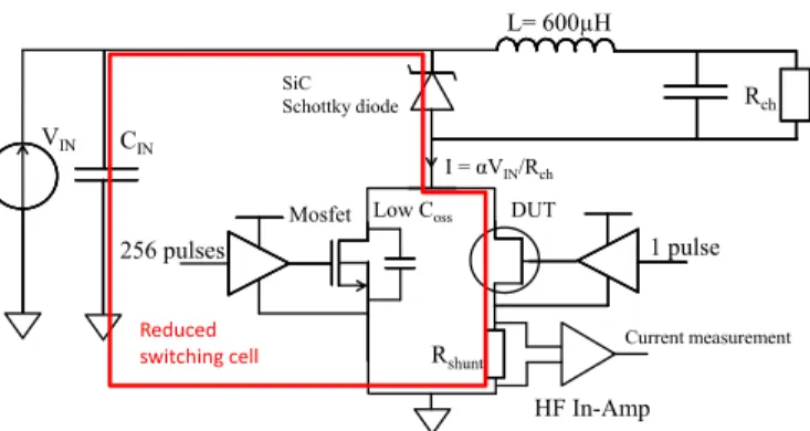
Figure 2. Schematic of the special pulse mode buck converter for switching characterization
This method is based on the specific buck converter detailed on Fig. 2. It consists of the DUT, a high voltage Mosfet, a SiC schottky diode, an inductance L, a capacitance CIN and a sense
resistor Rshunt. Contrary to the double pulse characterization
method, the current in the large inductance is not established by the DUT but an auxiliary Mosfet in parallel with the DUT. All current establishment constraints are now supported by this auxiliary mosfet and not more by the DUT. So the auxiliary Mosfet smoothly establishes the desired current and once the steady state operating point is established, the DUT switches only once as it shown by Fig. 3.
When the Mosfet establishes the current, the converter is working as a classical buck converter. The average current circulating into the converter is given by (3). It depends on the duty cycle α, the input voltage VIN and the charge Rch. So for a
given input voltage the current can be easily tuned by varying the charge or the duty cycle. While for double pulse method is the duration of the first pulse which sets the current.
𝐼 =𝛼𝑉𝐼𝑁
𝑅𝑐ℎ
A safe start-up is implemented to quickly reach the steady state and protect switches against overcurrent. Indeed we can notice on the blue waveform of Fig. 3 that the duty cycle is gradually increased before the steady state. Once the steady state is reached, in less than 3ms on Fig. 3, the DUT switches one time at the desired frequency. A cooling period is then set, where both auxiliary mosfet and DUT are in OFF state, and the stored energy in the inductance is fully discharged. Allows no current is flowing through the DUT during this cool down, one has to be careful that the leakage current and more exactly the leakage power density within the DUT is kept to a very small value. After this cooling period the mosfet can re-establish the current and another DUT switching waveform can be captured (for example, every second or few seconds, for averaging purposes).
Since the whole buck converter is operating in a pulsed mode, the current rating of the auxiliary mosfet is strongly reduced. Thus undersized current rating allows to choose an auxiliary device with a low output capacitance which is important because it is added to the one of the DUT. Another strong advantage of this technique is that the operating point on the DUT can be separately set for the switched current and switched voltage, independently from thermal considerations.
1 long pulse + 1 short pulse VIN CIN L= 600µH SiC Schottky diode DUT Id Rshunt 1 pulse 256 pulses VIN CIN Rch L= 600µH SiC Schottky diode Mosfet DUT I = αVIN/Rch Rshunt HF In-Amp Low Coss Current measurement Reduced switching cell
Figure 3. Waveforms of the special buck converter
B. Electro-thermal modelisation for evaluation of the switching characterization thermal stress
With the proposed special pulse mode buck converter the DUT conducts and so generates self-heating for only one short pulse contrary to the double pulse characterization method. To evaluate the drastic reduction of the DUT junction temperature during its characterization an electro-thermal simulation has been done.
A thermal model of a GaN on Si device is represented on the Fig. 4. It consists of the GaN on Si device soldered into a copper case. The heat capacity Cth and the thermal resistance
Rth of this model are calculated from (4) and (5) with c the
specific heat (J/(g°K)), ρ the density (g/m3), d the thickness (m),
S the surface (m²) and λth the thermal conductivity (W/(m·°K)).
𝐶𝑡ℎ= 𝑐 ⋅ 𝜌 ⋅ 𝑑 ⋅ 𝑆
𝑅𝑡ℎ= 𝑑
𝜆𝑡ℎ⋅𝑆
The heat is generated on the top of this device by the current crossing through the two-dimension electron gas (2DEG) and the contact resistances. This heat is evacuated by the Si substrate and then by the copper case. The heat evacuated through wires bonded on the device is not taken into account to simplify and because their thermal resistance are too important compared to the Si substrate. Finally the heat pass through a resistance RthJS and capacitance CthJS of the Si substrate equal to
1.43 °K/W and 1.34 mJ/°K, RthSC and CthSC of the soldered joint
of 3 °K/W and 0.18 mJ/°K, RthCA and CthCA of the chosen
TO-220 case equal to 40 °K/W and 0.54 J/°K [7].
The thermal model of the GaN on Si device is put into the electro-thermal model of Fig. 5. The double pulse method and our special pulse mode buck converter method are getting together for easier comparison. With this model the current in the inductance is set by a first DUT and when the desired
Figure 4. Thermal model of a GaN on Si device soldered into a copper case
Figure 5. Electro-thermal model getting together the double pulse method and the special pulse mode buck converter method
current is reached a second DUT switch it just one time at the desired frequency. Thus this electro-thermal model allows to evaluate self-heating of the DUT establishing the current in the double pulse characterization method and self-heating of the DUT switching one time at the desired operating point as in the pulse mode buck converter method.
IV. RESULTS
A. A specific switching characterization for evaluation of operating point and temperature impacts
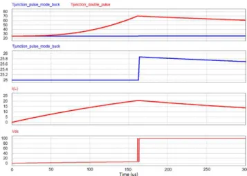
The DUT junction temperature comparison during its switching characterization by the double pulse method and by the special pulse mode buck converter is based on the electro-thermal model of the Fig. 5.
The results of the electro-thermal simulation are presented by the Fig. 6. The chosen DUT for the thermal stress comparison is an experimental partially package 200V/20A GaN on Si substrate device with an on resistance of 300mΩ shown on Fig. 4 and Fig. 7. When switching 100V/20A at 25°C the DUT reaches 70°C due to self-heating before switching during the first pulse of the double pulse characterization method. While it stays under 26°C in the worst case with the pulse mode buck converter method.
So the proposed switching characterization method allows to evaluate the switching performances at the desired operating point without significant self-heating and so independently of
Figure 6. Comparison of junction temperature for DUT switching characterization with the double pulse method and the proposed method
Auxiliary Mosfet
switchings
DUT switching
I
L400µs
Copper case
Si AlGaN/GaN RthJS RthSC RthCA 2DEG 5µm 400µm 50µm CthJS Soldered joint CthCA 2mm² Cthsc Electric ThermalFigure 7. Photograph of the special pulse mode buck converter
the temperature impact. The switching characterization circuit and process can even be simplify and optimized by removing the need of an effective thermal conductive packaging for the DUT.
B. Impacts of the operating point and temperature on a wide bandgap device
A photograph of the special pulse mode buck converter is shown on Fig. 7. A special attention was paid on the switching cell with the DUT to precisely evaluate switching performances of WBD by reducing the parasitic inductances. Moreover a low output capacitance mosfet has been chosen to limit the impact of an additional capacitance between the drain and source of the DUT. The chosen IRF820 500V mosfet has a maximum continuous and peak current rating of 2.5A and 8A.So it has a low output capacitance Coss equal to 60pF.
The switching performances of a SiC JFET 1200V/20A has been studied with the proposed method until 250V/20A. The switching frequency of the special pulse mode buck converter has been set to 40 kHz. On the wide range of tested operating points the steady state is reached in less than 3ms by the auxiliary mosfet into the 600µH inductor, 100µF capacitor and 4Ω output resistor. The impacts of the operating point and temperature have been independently studied. The chosen SiC JFET having an on resistance of only 85 mΩ and an efficient thermal conductive case, the heat generated by the pulse mode converter characterization method is considered negligible.
Waveforms of the SiC JFET switching a current of 0,5A and 7A with a power supply voltage of 120V and a junction temperature of 25°C are represented on Fig. 8. When the switched current is fixed to 7A the DUT switches on 25ns while it switches on only 17ns when the current is equal to 0,5A.
The impact of temperature on switching characteristics has been also studied. The switched operating point is fixed by the auxiliary mosfet at 120V/4A on Fig. 8. The junction temperature is in the first case fixed at the ambient temperature. In the second case the DUT is under a 350°C and 300l/min air flow during many seconds before switching. The junction temperature is expected to be almost 300°C but currently we cannot precisely measure it. So a minimum estimation of 150°C has been chosen for junction temperature comparison. The difference of SiC JFET fall time is only 1.5ns between DUT switching under ambient temperature and DUT switching under a 350°C air flow.
Figure 8. Impact of the switched current (0,5A and 7A) and the temperature (25°C and over 150°C) on the switching characteristics for VIN=120V.
V. CONCLUSION
The impact of the double pulse switching characterization method on the DUT has been studied in this paper. It points out that for experimental high power density WBD without casing or with a poor thermal management this method generates self-heating depending on the operating point. A special DC-pulsed mode buck converter is presented. It consists of an auxiliary mosfet in parallel of the DUT which smoothly establishes, in less than 3 ms the desired current. Once the steady state operating point is established, the DUT switches one time. An electro-thermal simulation shows that the thermal stress due to the device characterization is considerably reduced. So the proposed switching characterization method allows to set independently the operating point of the temperature with experimental WBD contrary to the double pulse characterization method. A SiC JFET has been characterized on a wide range until 250V/20A and up to 150°C to study its switching characteristics dependency with this method. Once the operating point and temperature dependency of a WBD known a safer and more efficient control can be provided [8].
REFERENCES
[1] T. Funaki, M. Sasagawa, and T. Nakamura, “Multi-chip SiC DMOSFET half-bridge power module for high temperature operation”, in APEC 2012, p. 2525-2529
[2] T. Morita, et al., « 99.3% Efficiency of three-phase inverter for motor drive using GaN-based Gate Injection Transistors », in APEC 2011, p. 481 -484.
[3] S. Ji, D. Reusch, and F. C. Lee, « High frequency high power density 3D integrated Gallium Nitride based point of load module », in ECCE 2012, p. 4267–4273.
[4] N. Kaminski, « State of the art and the future of wide band-gap devices », in European Conference on Power Electronics and Applications EPE ’09, p. 1-9, 2009.
[5] B. Hughes, J. Lazar, S. Hulsey, D. Zehnder, D. Matic, and K. Boutros, « GaN HFET switching characteristics at 350V/20A and synchronous boost converter performance at 1MHz », in APEC 2012, p. 2506–2508. [6] K.Ammous, H.Morel and A.Ammous, “Analysis of Power Switching Losses Accounting Probe Modeling”, in IEEE Trans. On Instrumentation and Measurement, vol.59,no.12, Dec. 2010
[7] “Safe Operating Area Testing Without A Heat Sink”, Fairchild Semiconductor Application Note AN-7516, Aug. 1994.
[8] R. Grezaud, F. Ayel, N. Rouger, and J.-C. Crebier, “An Adaptive Output Impedance Gate Drive for Safer and More Efficient Control of Wide Bandgap Devices”, in WiPDA 2013, in press
Vgs (150°C) IL= 4A 120V Vgs (25°C) Vds (25°C) Vds (150°C) 5ns Vgs (0,5A) IL 120V Vgs (7A) Vds (7A) Vds (0,5A) 5ns