HAL Id: hal-00272789
https://hal.archives-ouvertes.fr/hal-00272789
Submitted on 11 Apr 2008HAL is a multi-disciplinary open access
archive for the deposit and dissemination of sci-entific research documents, whether they are pub-lished or not. The documents may come from teaching and research institutions in France or abroad, or from public or private research centers.
L’archive ouverte pluridisciplinaire HAL, est destinée au dépôt et à la diffusion de documents scientifiques de niveau recherche, publiés ou non, émanant des établissements d’enseignement et de recherche français ou étrangers, des laboratoires publics ou privés.
Structural, magnetic and mechanical properties of 5 µm
thick SmCo films for use in
Micro-Electro-Mechanical-Systems
Arnaud Walther, Kirill Khlopkov, Oliver Gutfleisch, Dominique Givord, Nora
Dempsey
To cite this version:
Arnaud Walther, Kirill Khlopkov, Oliver Gutfleisch, Dominique Givord, Nora Dempsey. Struc-tural, magnetic and mechanical properties of 5 µm thick SmCo films for use in Micro-Electro-Mechanical-Systems. Journal of Applied Physics, American Institute of Physics, 2008, 103, pp.043911. �10.1063/1.2840131�. �hal-00272789�
Structural, magnetic and mechanical properties of 5 µm thick SmCo films for
use in Micro-Electro-Mechanical-Systems
A. Walthera,b, K. Khlopkovc, O. Gutfleischc, D. Givorda and N.M. Dempseya
aInstitut Néel, CNRS-UJF, 25 rue des Martyrs, 38042 Grenoble, France
bCEA Léti - MINATEC, 17 rue des Martyrs, 38054 Grenoble, France
cIFW Dresden, Institute of Metallic Materials, Helmholtzstr. 20, 01069 Dresden, Germany
Abstract
5µm thick SmCo films were deposited onto Si substrates using triode sputtering. A study of
the influence of deposition temperature (Tdep ≤ 600°C) on the structural, magnetic and
mechanical properties has shown that optimum properties (highest degree of in-plane texture,
maximum in-plane coercivity and remanence (1.3 and 0.8 T, respectively), no film peel-off)
are achieved for films deposited at the relatively low temperature of 350°C. This temperature
is compatible with film integration into Micro-Electro-Mechanical-Systems (MEMS). The
deposition rate was increased from 3.6 to 18 µm/h by increasing the surface area of the target
from 7 to 81 cm2. Mechanically stable films could be prepared by deposition onto
pre-patterned films or deposition through holes in a mask.
INTRODUCTION
Thick films (1-500 µm) of hard magnetic materials have many potential applications in magnetic
MEMS [1]. Owing to their excellent intrinsic magnetic properties, rare-earth transition metal
alloys (Nd2Fe14B and SmCo based alloys) are very good candidate materials when high
performance magnets are required [2]. The choice of material depends on the application
requirements and processing constraints. From the point of view of the materials’ intrinsic
properties, NdFeB is the material of choice for high energy product films (theoretical (BH)max =
516 kJ/m3; maximum value reported for a film is 400 kJ/m3 [3]) while SmCo5 is the material of
choice for high coercivity films (µ0HA = 40 T; maximum coercivity reported for a film is 5.6 T
[4]). The choice of material may also be dictated by requirements for magnetic texture (i.e. a
preference for the magnetic easy axes to be in-plane or out-of-plane). Under non-epitaxial
conditions and for relatively thick films (≥ 1µm), NdFeB can be prepared with out-of-plane
texture [3,5-7] while SmCo alloys can be prepared with in-plane texture [5,8,9]. Finally, the
integration of such films into MEMS may dictate processing constraints such as a maximum
processing temperature of 400°C for integration of films onto substrates which already contain
integrated circuits (“above IC”). This limitation excludes NdFeB for this type of use, since it
needs to be processed at higher temperatures (either deposited above 500°C [6] or annealed
above 650°C [10]. However, integration of NdFeB is possible when the material is
deposited/annealed before other temperature sensitive components. Note that the majority of
published works on RE-TM films deal with films of thickness in the range of 100 nm - 1µm,
which are too thin for use in MEMS. A recent review of hard magnetic materials for MEMS
applications has been given in [11].
Three distinct hard magnetic phases of the SmCo system have been studied in film form:
SmCo5 [8,9,12,13], SmCo7 [13,14] and Sm2Co17 [12]. Enrichment in Co with respect to the
magnetocrystalline anisotropy [2]. Thus for applications in which very large coercivites are
not needed, SmCo7 and Sm2Co17 are the phases of choice. In-plane textured SmCo7 or
Sm2Co17 films have been used for biasing of yttrium iron garnet (YIG) [15], permalloy [16]
and Colossal Magneto Resistance (CMR) [17] films. More recently, two prototype
micro-actuators have been made with patterned isotropic Sm2Co17 films [18]. To our knowledge, the
mechanical properties of RE-TM films have not been reported to date. In this paper, a study
of the structural, magnetic and mechanical properties of SmCo7 films destined for use in
MEMS will be presented. Si substrates have been used for compatibility with standard
micro-technology processing, in contrast with the above cited studies on the applications of such
films [15-18], in which oxide substrates (typically Al2O3) were used.
EXPERIMENTAL DETAILS
A Sm23Co77 cast target of diameter 3 cm, was sputtered using a triode sputtering system (Ar
pressure ≈ 2x10⁻³mbar). Cr(50 nm) / SmCo (5 µm) / Cr (50 nm) films were deposited at a rate
of 3.6 µm/hour onto Si substrates at temperatures ≤ 600°C (note that even when no power is
sent to the substrate furnace, the substrate temperature gradually rises during deposition,
reaching a final value of about 200°C – films deposited under such conditions are labeled
“cold” deposited). Post-deposition annealing was carried out ex-situ in a vacuum of 10-5mbar.
XRD structural characterization was carried out in both θ-2θ and pole figure configurations
using Co and Cu radiations, respectively. Observations and analysis were made with an
FEG-SEM (Gemini 1530) equipped with an EDX detector. Room temperature magnetic properties
were measured using a vibrating sample magnetometer. Film curvature was measured using a
RESULTS AND DISCUSSION
Structural properties
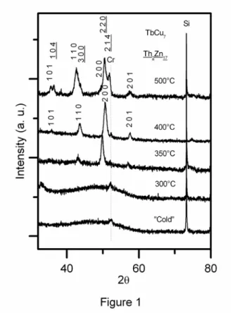
The θ-2θ XRD patterns of the as-deposited films are shown in figure 1. For Tdep ≤ 300°C, the
films appear to be amorphous (only Si and Cr peaks observed). Additional diffraction peaks
of the films deposited at 350°C and 400°C may be indexed as the TbCu7 structure while the
films deposited at 500°C have peaks of both the TbCu7 and Th2Zn17 structures. Munakata et
al. also observed the transition to a Sm poorer phase on increasing the deposition temperature,
though in their case the shift was from SmCo5 to Sm2Co17 [19]. The position of the (hk0)
peaks of the TbCu7 phase, which are dominant because of in-plane texture (see below), was
found to vary with deposition temperature, initially shifting to higher angles when the
deposition temperature increases from 350 to 400°C and then shifting to lower angles when
the deposition temperature is increased to 500°C. The value of the “a” lattice parameter was
estimated to be 4.9Å, 4.82Å and 4.9Å for Tdep = 350°C, 400°C and 500°C, respectively,
compared to a=4.997 Å for the SmCo5 phase [20]. This variation with deposition temperature
is attributed to an initial reduction in Sm content of the TbCu7 phase (presumably due to Sm
evaporation at the higher deposition temperature) and then a re-enrichment of the Sm content
of the TbCu7 phase caused by the appearance of the Th2Zn17 phase which is richer in Co. Note
that while EDX analysis indicates an average film composition of Sm14Co86, the resolution of
our EDX analysis was not precise enough to verify the assumption concerning the overall
shift in composition as a function of the deposition temperature.
Comparison of the relative intensities of the diffraction peaks of the θ−2θ scans indicates that the c axes of the TbCu7 phase are preferentially oriented in the plane, with the degree of
texture decreasing with increasing deposition temperature. The in-plane texture was further
evidenced using pole-figure analysis (figure 2). While the films deposited at 350°C have
deposited at 500°C are only weakly textured, with the (1 1 0) pole figure being sharper than
the (200) pole figure. In contrast with the strong (200) texture observed here, several literature
reports refer to (110) texture for SmCo5 [19,21] and SmCo7 [14,22]. Though there have been
studies reporting the influence of single parameters on the predominance of (200) or (110)
texture (e.g. oxygen level [23], sputtering pressure [13,22], deposition rate [24,25]), the
texture is most probably determined by a combination of many factors. Indeed the cited
reports on the influence of deposition rate are contradictory [24,25]. Broadening of the XRD
peaks was observed with increasing deposition temperature and may be due to a combination
of grain size reduction (it is plausible that the grain size of the 1:7 phase may decrease when
grains of the 2:17 phase form) and strain. Considering only grain size, Scherrer formula
analysis of Gaussian fits of the (2 0 0) peak of the 1-7 phase indicates that the crystallite size
of this phase decreases with increasing deposition temperature, from 16.5 nm at 350°C to 5
nm at 500°C. However the validity of these estimates is questionable because of the high
strain levels measured in these films (see below).
AFM analysis indicates that the films deposited up to 400°C are very smooth (RMS
roughness ≈ 2 nm) while those deposited at 500°C are rougher with an RMS ≈ 10 nm (images not shown). In most cases, attempts to observe the grain structure by high resolution
SEM-FEG imaging of fracture surfaces of the films’ cross sections were unsuccessful, presumably
owing to the absence of brittle fracture. Nevertheless, some microstructural features were
observed in the film deposited at 500°C. Roughly equiaxed grains with diameters of the order
of 80nm were observed on an internal surface which was revealed by film fracture
(presumably the void was formed due to the presence of a dust particle on the substrate)
(Figure 3a). A grain structure with comparable feature size was observed in plane-view
observing the microstructure of our SmCo7 films is coherent with the fact that clearly resolved
images of typically oblong grains have only been reported for SmCo5 films [13,19,26].
Magnetic properties
The magnetic properties were found to depend strongly on the deposition temperature. Films
deposited at temperatures ≤ 300°C (data not shown) are magnetically soft, in agreement with
the absence of x-ray diffraction peaks in these films. The in-plane (ip) and out-of-plane (oop)
hysteresis loops of films deposited in the range 350-500°C are shown in figure 4a-c. The
degree of magnetic texture, as characterized by the difference between the ip and oop
hysteresis loops, was found to decrease with increasing deposition temperature. In agreement
with the XRD data, in-plane texture is found (i.e. the magnetically easy c-axes are
preferentially aligned in the plane of the film). For the best textured film (Tdep=350°C),
Mr(ip)/M8T(ip) ≈ 0.83, Mr(ip)/Mr(oop) ≈ 12 and the absolute value of remanance is estimated
to be 0.8T. For a uniform distribution of the c-axes within the film plane, Mr(ip)/Ms(ip)= 2/π
≈ 0.64 for a system of non-coupled grains. Thus, the high value of Mr(ip)/M8T(ip) measured in
this system, indicates that the grains are exchange coupled. The shift of the out-of-plane loop
indicates that not all grains have been reversed under the maximum applied field of 8T. The
in-plane loop of the sample deposited at 500°C is characterized by the presence of two phases
(distinguished because of their different values of coercivity), in agreement with the XRD
data (i.e. SmCo7 and Sm2Co17). The coercivity of the films in their as-deposited state drops
from a value of 1.3T for Tdep = 350°C to a value of 0.5 T for Tdep = 500°C. Thus, 350°C
appears to be the optimum deposition temperature as it gives the maximum values or
coercivity and remanence and the films produced at this temperature have an estimated energy
Post-deposition annealing at a temperature of 750°C for 10 minutes leads to crystallization
and thus the development of coercivity in samples deposited at Tdep ≤ 300°C and to an
increase in coercivity and squareness for films which were deposited in the crystallized state
(Figure 5). The improvement in squareness leads in an increase in the energy product of the
film deposited at 350°C from 112 J/m3 in the as-deposited state to 144 kJ/m3 in the annealed
state. This energy product is to be compared with values of 90 kJ/m3 reported for isotropic
Sm2Co17 films [18], 120 kJ/m3 reported for textured SmCo5 [13] and SmCo7 [14] films and
206 kJ/m3 reported for textured Sm2Co17 films [27], all of which have thicknesses comparable
to the films studied here.
Influence of target size
A benefit of working with the triode sputtering technique is that the target size can be easily
varied. Following the above study, a larger target (9 x 9 cm2) of the same composition was
used so as to increase the deposition rate and to extend the zone of homogeneous film
thickness on the substrate. This increase in target surface area (from 7 cm2 to 81 cm2) raised
the deposition rate from 3.6 µm/h to 18 µm/h. This deposition rate is significantly higher than
the maximum values previously reported for SmCo films (5 µm/h [9,13], 10 µm/h [18]).
Furthermore, the high rates of deposition are achieved over relatively large areas: films
deposited on 100 mm Si wafers are only 20% thinner at the perimeter than at the centre. The
deposition rate and zone of homogeneous thickness are important factors for assessing the
suitability of a given technique for integrating films into MEMS.
Film deposition with the large target at the temperature which proved to be optimum for the
small target (350°C) produced samples with relatively poorer properties (lower coercivity and
lower squareness) and it was found that the magnetic properties could be improved by
kJ/m3 was reached for the optimum deposition temperature (400°C). The degree of (200)
texture was found to decrease with increasing deposition temperature, in agreement with the
results obtained with the small target (Figure 7). A comparison of the results for the two
different target sizes reveals an influence of deposition rate on growth mechanisms.
Mechanical properties
The mechanical properties of the as-deposited films were found to depend on the substrate
temperature during film deposition. While films deposited at temperatures of up to 400°C
remained entirely adhered to the Si substrate, small pieces (typically a few mm2) of those
deposited at 500°C peeled off and finally films deposited at 600°C almost entirely peeled off.
All as-deposited films were found to be under tensile stress and the resulting curvature was
measured using a profilometer on samples of typical size 1 cm2. The values of curvature were
then used to estimate the residual tensile stress using the Stoney formula [28]. Tensile stress
as a function of deposition temperature for the films deposited with the small target is plotted
in figure 8. The size of the error bars indicates the difference in stress values measured along
orthogonal directions.
Post-deposition annealing led to film peeling for all deposition temperatures. This peel-off is
attributed to the difference in thermal expansion coefficients of the SmCo layer and the Si
wafer and is the reason why most studies of thick films were made on substrates other than Si
[9, 15, 18] (thermal expansion coefficients of 6x10⁻⁶/K and 12 x10-6/K have been measured
parallel and perpendicular to the c-axis of SmCo5 at 600°C [29] while Si has a value of 2.6
x10-6/K). Peeling was found to be related to the lateral dimensions of the film. When 5 µm
thick SmCo films were deposited onto pre-patterned Si/SiO wafers which have topographic
relief (trench motifs with individual trenches of depth 5 µm with trench/wall widths on the
the scale 5-100 µm. Furthermore, films of thickness up to 20 µm deposited onto Si through a
mask with 4 x 4 mm sized holes remained adhered to the substrate and were crack free. These
results are reminiscent of those obtained on NdFeB films [3].
CONCLUSIONS
Triode sputtering has been used to deposit thick SmCo films (5 – 20 µm) onto Si substrates.
Deposition rates of 3.6 and 18 µm/h have been achieved for target surface areas of 7 cm2 and
81 cm2, respectively. A study of the influence of deposition temperature reveals that relatively
low deposition temperatures (350-400°C) are optimal with respect to structural, magnetic and
mechanical properties (highest degree of in-plane texture, maximum coercivity and maximum
remanence, no film peel-off). These relatively low temperatures are compatible with “above
IC” processing, and establish the potential for the integration of such films into MEMS. Film
peel-off due to strain can be avoided by the preparation of films with reduced lateral
dimensions (i.e. deposition through masks or onto pre-patterned substrates).
ACKNOWLEDGMENTS
This work was carried out in the framework of the ANR “Nanomag2” project. The authors
would like to thank A. Lienard and L. Ortega for technical assistance. K. K. is grateful for
financial support from DFG (SFB 463) and O. G. for a CNRS visiting research fellowship at
REFERENCES
[1] O. Cugat, J. Delamare and G. Reyne, IEEE Trans. Mag. 39, 3608 (2003)
[2] O. Gutfleisch, J. Phys. D: Appl. Phys. 33, R157 (2000)
[3] N.M. Dempsey, A. Walther, F. May, D. Givord, K. Khlopkov and O. Gutfleisch, Appl.
Phys. Lett. 90, 092509 (2007)
[4] J. Zhang, Y.K. Takahashi, R. Gopalan, K. Hono, J. Magn. Magn. Mater. 310, 1 (2007)
[5] F.J. Cadieu, J. Vac. Sci. Tec. A 6, 1668 (1988)
[6] B.A. Kapitanov , N.V. Kornilov, Ya.L Linetsky, and V.Yu. Tsvetkov, J. Magn. Magn.
Mater. 127, 289 (1993).
[7] L.K.E.B. Serrona, R. Fujisaki, A. Sugimura, T. Okuda, N. Adachi, H. Ohsato, I. Sakamoto,
A. Nakanishi, M. Motokawa, D.H. Ping and K. Hono, J. Magn. Magn. Mater. 260, 406 (2003)
[8] H. C. Theuerer, E. A. Nesbitt and D. D. Bacon, J. Appl. Phys. 40, 2994 (1969)
[9] R.P. Allen, S.D. Dahlgren, H.W. Arrowsmith and J. P. Heinrich, Technical report
AFML-TR-74-87 (1974)
[10] A. Walther, K. Khlopkov, O. Gutfleisch, D. Givordand N.M. Dempsey, J. Magn. Magn.
Mat. 316, 174 (2007)
[11] O. Gutfleisch and N.M. Dempsey, in Magnetic Nanostructures in Modern Technology,
edited by G. Asti, L. Pareti and M. Ghidini, (Springer, 2007), p. 167.
[12] F.J. Cadieu, S.H. Aly and T.D. Cheng, J. Appl. Phys. 53, 2401 (1982)
[13] T. Speliotis and D. Niarchos, J. Mag. Mag. Mat. 290, 1195 (2005)
[14] F.J. Cadieu, H. Hedge and K. Chen, J. Appl. Phys. 67, 4969 (1990)
[15] F. J. Cadieu, H. Hegde, E. Schloemann and H. J. Van Hook, J. Appl. Phys. 76, 6059
[16] H, Hegde, S. U. Jen, K. Chen, and F. J. Cadieu, J. Appl. Phys. 73, 5926 (1993)
[17] V. Neu, A. Anane, S. Wirth, P. Xiong, S. A. Shaheen and F. J. Cadieu, J. Appl. Phys. 87,
5350 (2000)
[18] T. Budde and H. H. Gatzen, J. Appl. Phys. 99, 08N304 (2006)
[19] M. Munakata, K. Goto and Y. ShimadaJpn. J. Appl. Phys. 23, L749 (1984)
[20] Powder Diffraction File 27-1122
[21] E. Pina, M.A. Garcıa, I. Carabias, F.J. Palomares, F. Cebollada, A. de Hoyos, R.
Almazan, M.I. Verdu, M.T. Montojo, G. Vergara, A. Hernando, and J.M. Gonzalez, J. Magn.
Magn. Mater. 272, e833 (2004)
[22] H. Hegde, P. Samarasekara, R. Rani, A. Navarathna, K. Tracy, and F. J. Cadieu, J. Appl.
Phys. 76, 6760 (1994)
[23 ] F.J. Cadieu, S.H. Aly, T.D. Cheng and L. Wickramasekara, J. Appl. Phys. 53, 8338
(1982)
[24] S.H. Aly, T.D. Cheung, L. Wickramasekara and F. J. Cadieu, J. Appl. Phys. 57,
2147(1985)
[25] R. Rani, F. J. Cadieu, X. R. Qian, W. A. Mendoza, and S. A. Shaheen, J. Appl. Phys.
81, 5634 (1997)
[26] V. Neu and S. A. Shaheen, J. Appl. Phys. 86 7006 (1999).
[27] F.J. Cadieu, J. Appl. Phys. 61, 4105 (1987)
[28] G. G. Stoney, Proc. R. Soc. London, Ser. A 82, 172 (1909)
[29] C. H. Chen, M. S. Walmer, M. H. Walmer, W. Gong and Bao-Min Ma, J. Appl. Phys. 85,
669 (1999)
FIGURE CAPTIONS
Figure 1: θ-2θ XRD patterns of the as-deposited SmCo films as a function of deposition temperature.
Figure 2: (110) and (200) pole figures of SmCo films deposited at (a) 350°C and (b) 500°C.
Note that the maximum intensity of the (2 0 0) pole figure of the sample deposited at 350°C is
10 times greater than that of the other pole figures.
Figure 3: SEM-FEG images of a SmCo film deposited at 500°C taken with an in-lens
detector: (a) cross sectional image of a fractured film; (b,c) plane-view images after Ar ion
etching of the Cr capping layer.
Fig 4: In-plane (ip) and out-of-plane (oop) hysteresis loops of SmCo films deposited in the
temperature range 350-500°C.
Figure 5: In-plane hysteresis loops of films annealed at 750°C for 10 minutes as a function the
Figure 6: Comparison of the in-plane hysteresis loops of SmCo films deposited in the
temperature range 350 - 400°C using a large (9x9 cm2) target.
Figure 7: Comparison of the φ−2φ xrd patterns of SmCo films deposited in the temperature range 350 - 400°C using a large (9x9 cm2) target.
Figure 8: Influence of deposition temperature on the tensile stress of SmCo films. The size of