HAL Id: tel-01323953
https://tel.archives-ouvertes.fr/tel-01323953v2
Submitted on 15 Jun 2016HAL is a multi-disciplinary open access
archive for the deposit and dissemination of sci-entific research documents, whether they are pub-lished or not. The documents may come from teaching and research institutions in France or abroad, or from public or private research centers.
L’archive ouverte pluridisciplinaire HAL, est destinée au dépôt et à la diffusion de documents scientifiques de niveau recherche, publiés ou non, émanant des établissements d’enseignement et de recherche français ou étrangers, des laboratoires publics ou privés.
the research of optical and electrical properties on
nanowire LED and photodetector
Hezhi Zhang
To cite this version:
Hezhi Zhang. the research of optical and electrical properties on nanowire LED and photodetector. Optics / Photonic. Université Paris Saclay (COmUE), 2016. English. �NNT : 2016SACLS096�. �tel-01323953v2�
= NNT : 2016SACLS096
T
HESE DE DOCTORAT
DE
L’UNIVERSITE PARIS-SACLAY
PREPAREE A
UNIVERSITE PARIS-SUD
ECOLE DOCTORALE N° 575
Eletical, Optical, Bio-physics and Engineering (EOBE)
Institut d’Électronique Fondamentale (IEF)
Spécialité de doctorat PHYSIQUE
ParHezhi Zhang
la recherche des propriétés optiques et électriques sur les nanofils LEDs et
photodétecteur
Thèse présentée et soutenue à Orsay, le 10 Mai 2016:
Composition du Jury :
M, Julien, François Directeur de recherche Président
UNIVERSITE PARIS-SUD
M, Schwarz, Ulrich professor Rapporteur TU Chemnitz
M, Larrieu, Guilhem Chargé de recherche Rapporteur LAAS
Mme, Tchernycheva, Maria Chargé de recherche Directeur de thèse UNIVERSITE PARIS-SUD
Mme Blandine Alloing Chargé de recherche Invité
CHREA
M, Christophe Durand Chargé de recherche Invité
Université Paris-Saclay
Espace Technologique / Immeuble Discovery
Route de l’Orme aux Merisiers RD 128 / 91190 Saint-Aubin, France
Titre : la recherche des propriétés optiques et électriques sur les nanofils LEDs et photodétecteur Mots clés : diodes électroluminescentes (LED), photodétecteurs, nanofils, InGaN / GaN, structure
cœur/coquille
Résumé : Le premier chapitre résume brièvement les propriétés de base des semi-conducteurs nitrures et décrit les méthodes d’élaboration des nanofils. Dans le deuxième chapitre, je présente mon travail sur la fabrication et la caractérisation de LED à nanofil unique InGaN/GaN ayant un contact transparent en graphène pour l’injection des trous.
Dans le troisième chapitre, je décris la fabrication et la caractérisation des LEDs à nanofils uniques fabriqués à partir d'une matrice de nanofils verticaux avec une morphologie des contacts identique à celle mise en œuvre pour les LEDs à base d’ensemble de nanofils.
Le dernier chapitre est consacré à l'étude des photodétecteurs à nanofils de nitrure. Je décris d'abord la fabrication et la caractérisation d'un photodétecteur de rayonnement ultraviolet basé sur un ensemble de nanofils de GaN avec un contact transparent en graphène. Ensuite, des détecteurs à nanofils uniques InGaN / GaN ont été fabriqués fonctionnant dans la gamme spectrale du visible à ultraviolet. Dans la dernière partie, je présente une technique pour la fabrication de photodétecteurs flexibles basée sur des ensembles de nanofils verticaux et je discute leurs performances.
Title : the research of optical and electrical properties on nanowire LED and photodetector
Keywords : light emitting diodes (LEDs), photodetectors, nanowires, InGaN/ GaN, core/shell
structure
Abstract : First chapter briefly summarizes the
nitride semiconductor basic properties and discusses the present status of nanowire elaboration. In the second chapter, I present my work on the fabrication and in-depth characterization of single nanowire InGaN/GaN LEDs with a transparent graphene contact for hole injection. Reference single wire LEDs with metal contacts are also investigated for comparison.
In the third chapter, I describe the fabrication and characterize single wire LEDs made out of a vertical NW array with the contacting scheme identical to array LEDs. The dependence of the electroluminescence on the contact morphology opens the way to control the LED emission color at the device processing stage.
The last chapter is dedicated to the study of nitride nanowire photodetectors. I first describe the fabrication and characterization of a GaN ultraviolet (UV) photodetector based on a NW array with a transparent graphene contact. Moreover, single NW InGaN/GaN detectors were fabricated operating in the visible to ultraviolet spectral range. In the last part, I present an up-to-date technique for fabricating flexible photodetectors based on vertical NW arrays and I discuss their performances.
I
Table of Contents
Abstract………IV
Résumé
..……….…………..….VIChapter 1 General Introduction
………..……….………..…..1
1.1 Basic properties of III-nitride semiconductors….………..………1
1.1.1Crystalline structure….……….1
1.1.2 Material properties of wurtzite III-nitride structure..………...3
1.1.3 Polarity of III-nitride materials..……….…….5
1.2 Growth of GaN nanowires.………...10
1.2.1 Catalyst-assisted “ vapor-liquid-solid” (VLS) growth….………..10
1.2.2 Catalyst-free GaN nanowires growth ………14
I.Molecular beam epitaxy (MBE) growth……….14
II.Metal Organic Chemical Vapor Phase Deposition (MOCVD) growth .... ………...17
1.3 Conclusion ... ………...21
Chapter 2 In-plane InGaN/GaN Core−Shell Single Nanowire Light
Emitting Diodes with Graphene-BasedP-Contact ... ………...27
2.1 Introduction ... ………...27
2.2 InGaN/GaN core-shell nanowire growth and sample structure………30
2.3 Optical properties………..32 2.3.1 Photoluminescence spectroscopy ... ………32 2.3.2 Cathodoluminescence spectroscopy ... ………32 2.4 Device fabrication ... 34 2.5 Device characterization ... 36 2.5.1 Electrical characterization………..36
2.5.2 Electron beam induced current characterization ... ………...37
2.5.3 Electroluminescence characterizations ... ………...40
II
2.6 Electrical model of the nanowire LEDs………44
2.7 Conclusion………50
Chapter 3 characterization of vertical single and array NWs LEDs…...….54
3.1 Nanowires growth method ... 56
3.2 Nanowire internal structure ... 56
3.3 Optical properties ... 57
3.3.1 Micro-photoluminescence spectroscopy ... 57
3.3.2 Cathodoluminescence spectroscopy ... 58
3.4 Single nanowire LEDs... 60
3.4.1 Fabrication of single nanowire LEDs ... 60
3.4.2 Electrical characterization of single nanowire LEDs ... 62
3.4.3 Electroluminescence of single nanowire LEDs ... 63
3.5 Array LED color control by a post-growth treatment ... 66
3.5.1 Processing of array LEDs with different contacting schemes ... 65
3.5.2 Electrical characterization of array LEDs with different contacting schemes ... 68
3.5.3 EBIC characteristics of array LEDs with different contacting schemes ... 69
3.5.4 Electroluminescence of array LEDs with different contacting schemes ... 70
3.6 EBIC signal transient at the core/under layer interface of n-GaN ... 73
3.7 Correlation between EBIC maps and electroluminescence maps ... 79
3.8 Front n-contact LED ... 81
3.9 Conclusions .... ………..87
Chapter 4: Nitride single nanowire and nanowire array photodetectors.... .91
4.1 GaN NW array ultraviolet photodetectors with a graphene transparent contact ... 94
4.1.1 NWs synthesis ... 94
4.1.2 Device fabrication ... 95
4.1.3 Device characterization ... 97
4.1.4 Conclusion ………..99
4.2 single InGaN/GaN core-shell NW photodetectors ... 100
III
4.2.2 Optical properties ... 102
4.2.3 Fabrication process of single InGaN/GaN core/shell NW photodetectors ... 103
4.2.4 Characterization of photodetectors with a localized metal contact ... 105
4.2.5 Characterization of photodetectors with ITO conformal contact ... 108
4.2.6 Conclusion ... 117
4.3 Flexible vertical InGaN/GaN core-shell NW photodiodes ... 119
4.3.1 Fabrication of the flexible photodetectors ... 119
4.3.2 Device characterization ... 120
4.3.3 Conclusion ... ………126
Chapter 5 General conclusion…..………..…………129
Appendix A: list of Abbreviations ... ...……….……….……….132
Appendix B: list of publication ... ...……….……….……….134
Appendix C: Code of silvaco of 30MQWs photodetector ...….……….136
IV
Abstract
III-nitride semiconductors have known a strong regain of interest at the end of 1990’s thanks to the successful demonstration of p-type doping, which has enabled a large palet of applications such as light emitting diodes (LEDs), laser diodes (LDs), photodetectors and solar cells. However, the material quality remains the key issue for thin film nitride devices. In the recent years, nanostructuring of the active region i the form of one-dimensional nanowires has been proposed as a primissing solution for the material quality problem. Indeed, the efficient strain relaxation allows to fabricate defect-free nanoobjects on lattice-mismatched substrates. In addition, the large lateral surface of nanowires allows to increase the absorption or emitting area by using core/shell heterostructures. Finally, growth along the non-polar m-plane nanowire facets suppresses the internal electrical field and enhances the absorption / emission efficiency.
In this manuscript, I present my work dedicated to the realization and characterization of nitride nanowire light emitters and detectors. I detail the device fabrication using state-of-the-art nanofabrication tools as well as the investigation of their electrical and optical properties.
First chapter briefly summarizes the nitride semiconductor basic properties and discusses the present status of nanowire elaboration. In the second chapter, I present my work on the fabrication and in-depth characterization of single nanowire InGaN/GaN LEDs with a transparent graphene contact for hole injection. Reference single wire LEDs with metal contacts are also investigated for comparison. The electroluminescence of single nanowire LEDs evidences the impact of the contact layout on the emission properties. In particular, the position of the contact determines the spectral evolution with injection current. Namely, for an extended contact and a contact localized on the m-plane, a transition from the green to blue emission is observed whereas for a localized contact on the m-plane/semipolar plane junction the emission remains green.
In the third chapter, I describe the fabrication and characterize single wire LEDs made out of a vertical NW array with the contacting scheme identical to array LEDs. The emission shows a similar evolution as the lateral-contacted single nanowire LEDs. The dependence of the electroluminescence on the contact morphology opens the way to control the LED emission color at the device processing stage. I used fluorine plasma treatment to reduce the conductivity of the p-doped GaN shell for inhibiting the electrical injection in the In-rich region of the quantum well. Furthermore, I analyze the injection
V
inhomogeneity effect. In order to avoid this effect, I developed a top down contacting scheme with electrons injected directly into n-GaN underlayer, which is called “front contacting” process. The “front contacting” LEDs show an enhanced yield of active nanowires from 19% to 65%.
The last chapter is dedicated to the study of nitride nanowire photodetectors. I first describe the fabrication and characterization of a GaN ultraviolet (UV) photodetector based on a NW array with a transparent graphene contact. Moreover, single NW InGaN/GaN detectors were fabricated operating in the visible to ultraviolet spectral range. The influence of the contact morphology is also investigated by comparing two types of contacts, namely a partial metal contact and an indium tin oxide (ITO) conformal contact, respectively. In the last part, I present an up-to-date technique for fabricating flexible photodetectors based on vertical NW arrays and I discuss their performances.
VI
Résumé
Les semi-conducteurs III-N ont connu un fort regain d'intérêt à la fin des années 1990 grâce à la démonstration du dopage p du GaN, qui a ouvert la porte à une grande palette d'applications notamment dans le domaine photonique avec des dispositifs comme les diodes électroluminescentes (LEDs), les diodes laser (LDs), les photodétecteurs et les cellules solaires. Cependant, la qualité du matériau reste le problème clé pour les dispositifs à couches minces de nitrure. Dans les dernières années, la nanostructuration de la région active sous forme de nanofils a été proposée comme une solution prometteuse pour améliorer considérablement la qualité du matériau. En effet, la relaxation des contrainte par les bords libres des nanofils permet de fabriquer des nano-objets sans défauts sur des substrats à fort désaccord de maille. En outre, la grande surface latérale des nanofils permet d'augmenter la surface d'absorption ou d'émission en utilisant des hétérostructures cœur/coquille. Enfin, la croissance sur des facettes m non polaires des nanofils supprime le champ électrique interne et améliore l'efficacité d'absorption / émission.
Dans ce manuscrit, je présente mon travail dédié à la réalisation et à la caractérisation des émetteurs et détecteurs de lumière à base de nanofils de nitrures. Je détaille la fabrication des dispositifs utilisant des outils de nanofabrication à l’état de l’art, ainsi que l'étude de leurs propriétés électriques et optiques.
Le premier chapitre résume brièvement les propriétés de base des semi-conducteurs nitrures et décrit les méthodes d’élaboration des nanofils. Dans le deuxième chapitre, je présente mon travail sur la fabrication et la caractérisation de LED à nanofil unique InGaN/GaN ayant un contact transparent en graphène pour l’injection des trous. L'électroluminescence des LEDs à nanofils uniques montre l'impact de la forme du contact sur les propriétés d'émission. En particulier, la position du contact détermine l'évolution spectrale avec le courant d'injection. À savoir, pour un contact étendu et un contact localisé sur le plan m, l’émission passe du vert au bleu en fonction du courant d’injection alors que pour un contact localisé sur la jonction entre le plan m et le plan semipolaire l'émission reste verte. Dans le troisième chapitre, je décris la fabrication et la caractérisation des LEDs à nanofils uniques fabriqués à partir d'une matrice de nanofils verticaux avec une morphologie des contacts identique à celle mise en œuvre pour les LEDs à base d’ensemble de nanofils. L'émission montre une évolution similaire à celle observée pour les LEDs à nanofils uniques avec un contact latéral. L’influence de la
VII
morphologie des contacts sur l'électroluminescence ouvre la possibilité de contrôler la couleur d'émission de la LED à l'étape de la fabrication. J'ai utilisé un traitement par plasma de fluor afin de réduire la conductivité de la coquille GaN dopé p et d’inhiber l'injection électrique dans la région riche en In du puits quantique. En outre, j'ai analysé l'effet de l’inhomogénéité d'injection. Afin d'améliorer l’homogénéité, j'ai développé un système de contact par le haut permettant d’injecter les électrons directement dans la sous-couche n-GaN. Les LEDs fabriquées selon cette procédure montrent un rendement amélioré avec 65% de nanofils actifs contre 19% pour une procédure standard.
Le dernier chapitre est consacré à l'étude des photodétecteurs à nanofils de nitrure. Je décris d'abord la fabrication et la caractérisation d'un photodétecteur de rayonnement ultraviolet basé sur un ensemble de nanofils de GaN avec un contact transparent en graphène. Ensuite, des détecteurs à nanofils uniques InGaN / GaN ont été fabriqués fonctionnant dans la gamme spectrale du visible à ultraviolet. L'influence de la morphologie de contact est également étudiée en comparant deux types de contacts, à savoir un contact métallique localisé et un contact étendu en oxyde d'indium-étain (ITO). Dans la dernière partie, je présente une technique pour la fabrication de photodétecteurs flexibles basée sur des ensembles de nanofils verticaux et je discute leurs performances.
Mot-clé: diodes électroluminescentes (LED), photodétecteurs, nanofils, InGaN / GaN, structure
1
Chapter 1 General Introduction
Table of contents
1.1 Basic properties of III-nitride semiconductors ... 1
1.1.1Crystalline structure ... 1
1.1.2 Material properties of wurtzite III-nitride structure ... 3
1.1.3 Polarity of III-nitride materials ... 5
1.2 Growth of GaN nanowires ... 10
1.2.1 Catalyst-assisted “ vapor-liquid-solid” (VLS) growth ... 10
1.2.2 Catalyst-free GaN nanowires growth ... 14
I.Molecular beam epitaxy (MBE) growth ... 14
II.Metal Organic Chemical Vapor Phase Deposition (MOCVD) growth ... 17
1.3 Conclusion ... 22
1.1 Basic properties of III-nitride semiconductors
First we focus on the basic materials properties of the III-nitride semiconductors. The nitride material family (gallium nitride (GaN), indium nitride (InN), aluminum nitride (AlN) and their alloys) is of major importance for optoelectronic devices. Other binary III-nitride compounds exist, like boron nitride (BN), but this material is far less used for devices, so it will not be discussed here. GaN, InN and AlN semiconductors share a certain number of common features.
1.1.1 Crystalline structure
A stable crystalline phase for nitride materials is the hexagonal phase with a wurtzite structure. Note that it is also possible to obtain a cubic zincblende phase for III-nitrides grown under certain conditions, however this cubic phase is metastable. The wurtzite structure is characterized by an AB
2
AB sequence along the [0001] direction. For the zincblende structure, it has an ABC ABC stacking in [111] direction. Each atomic layer is rotated in-plane by 30° with respect to the subsequent one. Due to this structural similarity, some structural defects like stacking faults allow the coexistence of hexagonal and cubic phase in the epitaxial layers.
Here we mainly talk about the hexagonal wurtzite structure since it is dominant in nanowires. The wurtzite structure follows the space group P63mc (C46v). A schematic of the wurtzite structure is
displayed in Fig. 1.2. The metal atom (Al, Ga and In) and nitrogen atoms are stacked in a hexagonal close-packed system, shifted one with respect to the other along the c-axis ( [0001] ). The edge length of the basal hexagon is named by a, the height of the hexagonal prism c and, the anion-cation bond length along the [0001] axis u. The ratio u/c is a measure of the non-ideality of the crystal in comparison to an ideal wurtzite structure with u/c = 3/8 = 0.375 in the ideal wurtzite lattice. Another measure of the non-ideality is the ratio of lattice constants c/a, which is equal to p=1.633 for an ideal wurtzite crystal.
Figure 1.1 Schematic drawings of the (a) AB AB and (b) ABC ABC stacking orders along the polar
3
1.1.2 Material properties of wurtzite III-nitride semiconductors
The importance of the III-nitrides for the optoelectronic industry comes from the fact that they are wide bandgap semiconductors. Their bandgap is direct, which allows for efficient light emission. According to data that adorned the literature for years, the established bandgap values are 0.6 eV for InN[1], 3.42 eV for GaN[2], and 6.0 eV[3] for AlN at room temperature. The variation of the band gap with temperature is given by the Varshni law[4]:
(1.1)
where Eg(0) is the bandgap energy at 10 K. The parameters α and β are tabulated in table 1.1, taking
into account the electron-phonon interaction.
u
a
c
4
Quantity symbol AlN GaN InN (Unit)
Crystal structure[2] W W W
Gap Direct Direct Direct
Lattice constant[2] A0= 3.112 3.189 3.545 Å Thermal expansion[2] 4.2 5.6 3.8 10-6/K Lattice constant[2] C0= 4.982 5.185 5.703 Å Thermal expansion[2] 5.3 3.2 2.9 10-6/K c/a[2] 1.601 1.626 1.680 u/c[2] 0.379 0.376 0.378 Bandgap energy[1][2][3] Eg= 6.0 3.42 0.6 eV
Varshni parameter[2] α 1.799 0.909 0.414 meV/K
β 1462 830 454 K
Table 1.1 summarizes the values of bandgap energy, Varshni parameters, the lattice parameters including a and c, the metal-N bond length u, and the c/a and u/c ratios for GaN, AlN and InN at room temperature. The thermal expansion coefficients are also displayed in table 1.1.
The bandgaps of the three binary compounds cover a broad spectral range (Table 1.1), from the ultraviolet (6.0 eV for AlN) to the infrared (0.6 eV for InN). For the majority of applications, combinations of binary compounds are used to synthesize ternary alloys. Their bandgaps vs lattice parameters are displayed in Figure. 1.3. The evolution of the bandgap of ternary alloys as a function of the composition is non-linear, they are bent following Eq. (1.2) for an A1−xBxN alloy
[2]
:
E
g(x) = E
g(AN)·
(1−x) + E
g(BN)·
x − b·x·(1−x) (1.2)
5
AlN-GaN GaN-InN AlN-InN
Alloy bandgap bowing[5][6][7] 0.62 1.43 4.9
Table 1.2 Bowing parameters of ternary alloys.
1.1.3 Polarity of III-nitride materials
The wurtzite structure has a polar axis due to the lack of a symmetry inversion center [8][9][10] (Figure 1.4). The polarity is determined by the direction of the vector associated to the metal-N bond along the [0001] axis. The c-axis is defined positive when such a vector points from the metal atom towards the N atom, as illustrated in Figure 1.4(a). In this case, the polarity of the crystal is called polarity [0001], metal or Al-, Ga-, In-polarity. The basal surface shows the cations (Al, Ga or In) on the top position of the (0001) bilayer. On the contrary, if the basal surface of the (0001) bilayer shows the N anions, the polarity corresponds to [000-1], or N-polarity.
Figure 1.3. Bandgap energy as a function of in-plane lattice parameter for III-nitrides compounds[5][6][7].
6
Since nitrogen atoms have a smaller atomic radius and higher ionization energy than metal atoms, nitrogen atoms are more electronegative than metal atoms and bonds can be considered as an electrostatic dipole. This charge distribution in the tetrahedron is not compensated by the atomic stacking because of the noncentrosymmetric nature along the [0001]-direction, resulting thus in a macroscopic spontaneous polarization ( Psp )
[11][12]
in nitride materials. Theoretical values of spontaneous polarization given by Vurgaftman et al[2]. are presented in Table 1.3. As seen in Fig. 1.4, Psp points from the metal- to the N-atom, being thus negative for metal-face and positive for N-face
crystals. The increase of the Psp magnitude in nitrides, from GaN to InN and finally to AlN, is related
to the deviation of the lattice from the ideal wurtzite structure given by the u/c and c/a parameters in Table 1.1.
AlN GaN InN
Spontaneous polarization ( C/m2 )[2] -0.09 -0.034 -0.042
Table 1.3 Spontaneous polarization for wurtzite-type GaN, AlN and InN.[2] Figure 1.4 Ga-face and N-face polarities in a wurtzite GaN structure.
7
Stress modifies the atomic positions in the crystal leading to a different spatial distribution of the charges and inducing a piezoelectric polarization ( Ppz )
[11][12]
. Usually, III-nitrides are grown on the (0001)-plane and the layers show a biaxial stress perpendicular to the [0001]-axis due to the lattice and thermal mismatch between the substrate and the layer. In this case, the piezoelectric polarization in each direction is given by[13][14]
Then, the piezoelectric field is positive (i.e. in the [0001]-direction) or negative (i.e. in the [000-1]-direction) if the material is under compressive strain (a < a0) or tensile strain (a > a0),
respectively. The total polarization of the layer is the sum of the spontaneous and piezoelectric polarizations. Table 1.4 shows the piezoelectric coefficients for III-nitrides [2].
AlN GaN InN
e31 ( C/m2 ) -0.50 -0.35 -0.57
e33 ( C/m2 ) 1.79 1.27 0.97
Table 1.4: Piezoelectric coefficients e31 and e33 for GaN, AlN and InN. [2]
Due to the discontinuity of the piezoelectric and spontaneous polarizations, the nitride heterostructures exhibit bound charges at the interfaces, which affect the properties of the whole structure as detailed below [14][15].
InGaN light emitting diodes (LEDs)[16][17] and laser diodes (LDs)[18][19] are based on a sandwich-type structure made of GaN/InGaN/GaN layers, where the difference in bandgap creates a quantum well (QW) structure, the so-called InGaN QW. The smaller bandgap of the InGaN layer leads to a trapping of the holes and electrons from the valence and conduction band, respectively. The recombination of
1.3
8
the excitons (electron-hole pairs) takes place in the InGaN QWs as schematically displayed in Figure 1.5 (a) showing an InGAN/GaN QW in the absence of internal field. The confinement leads to the quantification of the energy states in the QW. Usually the recombination occurs between the ground state in the QW conduction band and the heavy hole (A-band) in the valence band. On the other side, the above mentioned piezoelectric and spontaneous polarizations are important for polar structures. Indeed, the polarization discontinuity at the interfaces leads to building of surface charges, which create an electric field in the QWs. This results in a band-bending and leads to a red-shift of the emission wavelength[20], but also to a strong reduction in the overlap of the electron and hole wavefunctions as illustrated in Figure 1.5 (b). This effect is known as the Quantum Confined Stark Effect (QCSE). The reduced overlap strongly lowers the radiative-recombination probability and thus strongly affects the emission efficiency. While the red-shift allows one to reach longer wavelengths with lower indium content, the reduced efficiency is detrimental for the device performance.
Therefore, it is desirable to grow InGaN-GaN heterostructures with reduced or completely suppressed internal fields. This is possible by performing the growth on crystal facets perpendicular to the c-plane, i.e. for the {1-100} m- and {11-20} a- plane of GaN as shown in figure 1.6 (b) and (c). For facet orientations having an intermediate angle with the c-axis, the internal fields are typically reduced, but not zero (examples of these planes are shown in figure 1.6(a) to (e)); hence, the respective crystal planes are called ‘semipolar’. For about 10 years, the idea to reduce the internal fields by using non- or semipolar crystal facets has triggered a huge number of research studies worldwide[21][22][23][24][25][26]. Figure 1.5 Schematics of a single InGaN quantum well structure (a) without and (b) with internal electric field.
9
Among these studies, nanowire devices open a way to grown III-nitride material along m- plane or a-plane using the deposition on the sidewalls.
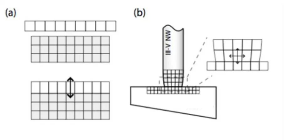
Another challenge present for the thin film growth is the large number of dislocations emerging during the growth due to the difference of lattice parameters with the substrate, which are called “misfit dislocations”[27]
. The most common dislocation type in wurtzite systems are threading dislocations which propagate through the whole film, from the interface with the substrate to the surface of the layer. The mismatch problem has less consequences on the crystal quality in nanostructures because of their small diameter allowing strain to be relaxed laterally (figure 1.7(b)) in contrast with the planar growth where strain can only be relaxed along one dimension (figure 1.7(a)). Indeed, defect free GaN nanowire growth has been demonstrated on highly mismatched substrate such as sapphire [28][29], and also low-cost substrates: Si (111) [30]and Si (001)[31].
10
1.2 Growth of GaN nanowires
1.2.1 Catalyst-assisted “vapor-liquid-solid” (VLS) growth
In 1964, Wagner and Ellis first described the VLS growth method on Si whiskers with Au as a catalyst
[32]
. The growth mechanism can be explained as follows: Si atoms enters the Au from the gas phase forming Au-Si alloy. As the Au drop becomes super-saturated, Si precipitates in solid form at the liquid/solid interface with the substrate, and crystal growth takes place selectively under the Au particle.
Figure 1.7 Illustration of the Si/III-V interface. (a) Planar growth for normal heterointerface, strain can only be relaxed along one dimension. (b) NW growth, strain can be relaxed laterally, allowing 3D strain relaxation.
11
Similar to Si, GaN nanorods have also been achieved by the VLS growth method by using Au [33][34], Ni [35] and Ta[36] as a catalyst. Figures 1.8 (a) and (b) illustrate GaN VLS growth method with Au [33]. Figure 1.8 (c) proves that most of GaN nanorods are well aligned vertically with respect to the Si (111) substrate.
Figure 1.8 (a) and (b) illustrate the GaN VLS growth method using an Au catalyst. (c) SEM image of GaN nanorods[33].
Figure 1.7 Schematic illustration of the VLS growth of Si wires using an Au catalyst particle. The grey arrow, and labels (i), (ii) and (iii) illustrate the different stages of nanowire growth
12
In 2004, Qian et.al[37] used these high quality p-type GaN nanowires to realize radial heterostructures for nanophotonics. The well-defined doped n-GaN/InGaN/p-GaN core/shell nanowire heterostructures provided a new strategy for efficient carrier injection. Photoluminescence (PL) data further show that the optical properties are controlled by the core/shell structure with a strong emission from the InGaN layer centered at 448 nm. Electrical measurements with separate contacts to the core and outer shell have demonstrated that these core-shell nanowires behave as p-n diodes with a blue light emission arising from the electron-hole recombination in the InGaN layer.
(a) (b)
Figure 1.9 (a) Synthesis of core-shell nanowire heterostructures. (b) Optoelectronic properties of
13
Nevertheless, the GaN nanowires grown via a VLS growth mode often present defects such as a tilt, twist, intersect and branch. For large scale and industrial solid-state lighting application, this growth method may not be suitable due to these defects as well as the difference in height and orientation of GaN nanorods.
14
1.2.2 Catalyst-free GaN nanowires growth
I. Molecular beam epitaxy growth
The GaN nanowires have been synthesized by catalyst-free plasma assisted molecular-beam epitaxy (MBE) growth. Several groups have reported the self-induced growth of GaN NWs on various substrates such as Si[30][31][38], sapphire[29], diamond[39] and silicon carbide (SiC)[40]. Figures 1.10 (a), (b), (c) and (d) show GaN NWs growth on Si, sapphire, diamond and SiC, respectively.
Among these substrates, single crystalline Si substrates are commonly used today to fabricate catalyst-free GaN NWs. The growth method and mechanism have been studied intensively. Bertness et al[41]. demonstrated that inserting an AlN layer buffer between the Si and GaN NWs is essential to The figures 1.10 (a), (b), (c) and (d) present SEM images of GaN NWs on Si[30][31][38], sapphire[29], diamond[39] and SiC[40], respectively.
(a)
(b)
15
improve the growth (in particular, the nanowire verticality) and the thickness of the buffer is also a key parameter for controlling morphology of the NWs. They discussed the nucleation mechanism and showed that the GaN nanorods nucleate not on top of the AlN layer, but are rather highly correlated with the formation of hexagonal pits with {1-102} facets
Furthermore, the growth processes was also investigated by Ristic et al[42]. During the nucleation process, the substrate surface is covered by GaN islands of different sizes as shown in figure 1.11 (a). When the nucleous reaches its critical size, the NW starts to grow on GaN islands. Some NWs start to grow earlier than others due to different nucleation times, resulting in a height dispersion. The Ga diffuses along the NWs sidewalls up to the apex. The wider the NWs, the slower is its growth rate. The following steps depend on two contributions 1) Ga atom impinging on the nanowire apex will incorporate directly to the crystal; 2) Ga atoms arriving to the substrate surface will diffuse to the
nanorods base, climb along the lateral sidewalls up to their apex and incorporate to the crystal as
shown by the diagram in Figure 1.11 (b).
For the MBE growth, the V/III ratio is also a critical parameter. Normally,a high aspect ratio GaN nanorod growth requires high V/III ratios. As illustrated in Figure 1.12, the high V/III ratio leads to a
GaN nanorod growth, while a low V/III (Ga-rich) allows a 2D layer growth [43].
16
Organized GaN nanocolumns grown by MBE have been fabricated by Hiroto et al[44]. They used patterned Ti film as a selective area growth (SAG) mask. The diameters of the mask openings were designed from 100 nm to 250 nm. They found that the selectivity can only be achieved at high temperature above 900 °C. The mechanism of SAG was simply explained in terms of the dependence of the desorption and diffusion of Ga adatoms on Ti.
Figure 1.13 The SEM image of GaN nanowires grown by MBE on a patterned Ti mask[44]. Figure 1.12 SEM micrographs of two GaN layers grown directly on Si (111) substrates under
17
The formation mechanisms of GaN nanowires grown by SAG has been explained in detail by Gacevic et al[45] who showed that the formation of SAG GaN NWs proceeded in two stages, driven by SAG kinetics and free-surface energy minimization, respectively. The first growth stage consists of the following three steps: initial nucleation at the nano hole inner periphery (driven by Ga adatom diffusion on a discontinuous surface), coalescence onset, and full coalescence, finishing when the growing nanocrystal fills the entire nanohole area. In the second growth stage, the nanocrystal undergoes morphological evolution through unstable cylindrical-like and dodecagonal shapes, ending when the thermodynamically stable hexagonal NW is formed.
II. Metal Organic Chemical Vapor Phase Deposition growth
GaN nanowires synthesis by MOCVD was first achieved on patterned templates. In 2006, Hersee et. al
[28]
presented the growth of high quality GaN nanowires and uniform nanowire arrays. For their experiment, a 30 nm silicon nitride mask was deposited on GaN film for defining the position of each GaN nanowire. A pulsed MOCVD was used allowing the nanowire diameter to remain constant after the nanowires had emerged from the selective growth mask. The SEM image of selective area growth GaN by MOCVD is shown in figure 1.15.
18
In 2010, the continuous-flux growth of GaN nanorod has been reported[46]. The nanorods were grown on a patterned sapphire with SiO2 mask layer. It was found that the nanowire structure is dependent on
the H2/N2 ratio. The lower H2/N2 ratio produces a pyramidal structure, while a higher H2/N2 ratio leads
to a nanorod structure growth. The diameter of nanorods is inversely proportional to the H2/N2 ratio.
Moreover, the morphology of GaN nanorods also has a strong relationship with Ga polar and N polar Figure 1.16 (a) Growth with pure nitrogen as carrier gas leads to pyramidal-shaped GaN growth,
(b) whereas nanorod growth occurs with H2/N2 carrier gas mixture of 1/2, and (c) still improves for
H2/N2 carrier gas mixture of 2/1
[46]
.
Figure 1.15 Scanning electron micrograph of a GaN nanorod array consisting of 1 μm GaN nanorods (The inset shows a top view and reveals the hexagonal symmetry of the nanorods). (b) A
19
nature of the crystal. In 2012, Li et al. reported nitrogen-polar core-shell GaN LEDs grown by selected area MOVPE[47]. The nanorods were grown on a SiO2 patterned N-polar GaN/sapphire subtrate. The
nanowires show clear vertical sidewalls and the top part has a flat platform, which is different with the growth on a Ga polar substrate. In 2013, the Ga polar GaN nanocolumn LED grown by continuous-flow MOVPE has been realized by Wang et. al[48]. The Ga polar LEDs show a pyramidal GaN structure, which has an evident {10-11} facet boundary. This can be explained by the fact that, for Ga polar orientation, the r-planes {10-11} or {10-1-1} are terminated by N atom, which can be passivated by hydrogen. Thus, the r-plane keeps stable and has a low growth rate.
Self-assemble GaN single-crystal nanowires have been reported in 2010 by Koester et.al[49]. The self-assembled nanowires are grown directly on c-plane sapphire without depositing neither a buffer layer nor a mask. The nanowire growth is promoted by a thin SiNx layer (2nm) to enable a vertical
growth of c-oriented wires with 200-1500 nm diameters. The GaN seed nucleation time determines the mean diameter and the structure quality.
20
Wang et al[50] reported the growth mechanism of catalyst-free self-organized GaN nuclei and three-dimensional columns on sapphire by MOVPE. They performed temperature and time dependent growth studies. They found that the growth behaviour can be characterized by two different kinetic regimes: mass-transport-limited growth and thermodynamically limited growth. The sum of the activation energies for the thermodynamic barrier of nucleation and for the surface diffusion/mass-transport limitation, i.e. Whet + Ed, is 0.57 eV in the ‘low’-temperature region and 2.43
eV in the “high”-temperature region. GaN columns grown under the same conditions have a comparable height, which is not dependent on their diameter or on the distance to other columns. Therefore, the growth rate is presumably limited by the incorporation rate on the top surface of columns. The height and diameter at the top of the GaN columns increase linearly with time and no height limit is observed.
21
Figure 1.19 The growth mechanism of catalyst-free self-organized GaN nuclei and three-dimensional columns on sapphire[50]
22
1.3 Conclusion
In this chapter, first I sumerize the basic physical properties of III-nitride materials. The wurtzite structure of III-nitride alloys leads to the strong internal electrical fields induced by spontaneous and piezoelectric polarizations, which significantly reduce the efficiency of optical devices such as solar cells or LEDs. One of the promising solutions to get rid of this effect is to make use of III-nitride NWs for devices. Several growth methods are reviewed including the VLS, and catalyse-free growth by MEB and MOCVD method. The different morphologies obtained are analyzed by controlling the growth conditions. In the next three chapters, I will present the NWs optical devices grown mainly by MOVPE and discuss their performance. I will provide the state of art for the different devices in the corresponding chapters.
23
References
[1] Haddad, D. B., et al. "Optical and electrical properties of low to highly-degenerate InN films."
MRS Proceedings. Vol. 798. Cambridge University Press, 2003.
[2] Vurgaftman, I., and J. R. Meyer. "Band parameters for nitrogen-containing semiconductors."
Journal of Applied Physics 94.6 (2003): 3675-3696.
[3] Silveira, E., et al. "AlN bandgap temperature dependence from its optical properties." Journal of
Crystal Growth 310.17 (2008): 4007-4010.
[4] Varshni, Yatendra Pal. "Temperature dependence of the energy gap in semiconductors." Physica 34.1 (1967): 149-154.
[5]Wu, J., et al. "Narrow bandgap group III‐nitride alloys." physica status solidi (b) 240.2 (2003): 412-416.
[6] Lee, S. R., et al. "The band-gap bowing of Al {sub x} Ga {sub 1 {minus} x} N alloys." Applied
physics letters 74.22 (1999).
[7] Terashima, Wataru, et al. "Growth and characterization of AlInN ternary alloys in whole composition range and fabrication of InN/AlInN multiple quantum wells by RF molecular beam epitaxy." Japanese journal of applied physics 45.6L (2006): L539.
[8] Northrup, John E., Jörg Neugebauer, and L. T. Romano. "Inversion domain and stacking mismatch [9] boundaries in GaN." Physical review letters 77.1 (1996): 103.
Hellman, E. S. "The polarity of GaN: a critical review." MRS Internet Journal of Nitride
Semiconductor Research 3 (1998): e11.
[10] Austerman, Stanley B., and William G. Gehman. "The inversion twin: prototype in beryllium oxide." Journal of Materials Science 1.3 (1966): 249-260.
[11] Bernardini, Fabio, Vincenzo Fiorentini, and David Vanderbilt. "Spontaneous polarization and piezoelectric constants of III-V nitrides." Physical Review B56.16 (1997): R10024.
[12] Ambacher, O., et al. "Role of Spontaneous and Piezoelectric Polarization Induced Effects in Group‐III Nitride Based Heterostructures and Devices."physica status solidi (b) 216.1 (1999): 381-389.
24
strained quantum wells." Japanese Journal of Applied Physics 36.4A (1997): L382.
[14] Yu, E. T., et al. "Spontaneous and piezoelectric polarization effects in III–V nitride heterostructures." Journal of Vacuum Science & Technology B 17.4 (1999): 1742-1749.]
[15] Waltereit, P., et al. "Nitride semiconductors free of electrostatic fields for efficient white light-emitting diodes." Nature 406.6798 (2000): 865-868.
[16] Nakamura, Shuji, Masayuki Senoh, and Takashi Mukai. "High‐power InGaN/GaN double‐heterostructure violet light emitting diodes." Applied Physics Letters 62.19 (1993): 2390-2392.
[17] Nakamura, Shuji, et al. "High-brightness InGaN blue, green and yellow light-emitting diodes with quantum well structures." Japanese Journal of Applied Physics 34.7A (1995): L797.
[18]Nakamura, Shuji. "The roles of structural imperfections in InGaN-based blue light-emitting diodes and laser diodes." Science 281.5379 (1998): 956-961.
[19] Nakamura, Shuji, et al. "InGaN-based multi-quantum-well-structure laser diodes." Japanese
Journal of Applied Physics 35.1B (1996): L74.
[20] Chichibu, S. F., et al. "Effective band gap inhomogeneity and piezoelectric field in InGaN/GaN multiquantum well structures." Applied Physics Letters73.14 (1998): 2006.
[21]Tyagi, Anurag, et al. "Semipolar (1011) InGaN/GaN laser diodes on bulk GaN substrates." Japanese journal of applied physics 46.5L (2007): L444.
[22]Enya, Yohei, et al. "531 nm green lasing of InGaN based laser diodes on semi-polar {2021} free-standing GaN substrates." Applied Physics Express2.8 (2009): 082101.
[23]Yeh, Ting-Wei, et al. "InGaN/GaN multiple quantum wells grown on nonpolar facets of vertical GaN nanorod arrays." Nano letters 12.6 (2012): 3257-3262.
[24]Koester, Robert, et al. "M-plane core–shell InGaN/GaN multiple-quantum-wells on GaN wires for electroluminescent devices." Nano letters 11.11 (2011): 4839-4845.
[25]Zhang, Hezhi, et al. "Color control of nanowire InGaN/GaN light emitting diodes by post-growth treatment." Nanotechnology 26.46 (2015): 465203.
[26]Tchernycheva, M., et al. "InGaN/GaN core–shell single nanowire light emitting diodes with graphene-based p-contact." Nano letters 14.5 (2014): 2456-2465.
25
[27]Ning, X. J., et al. "Growth defects in GaN films on sapphire: The probable origin of threading dislocations." Journal of materials research 11.03 (1996): 580-592.
[28] Hersee, Stephen D., Xinyu Sun, and Xin Wang. "The controlled growth of GaN nanowires." Nano
letters 6.8 (2006): 1808-1811.
[29] Wang, George T., et al. "Highly aligned, template-free growth and characterization of vertical GaN nanowires on sapphire by metal–organic chemical vapour deposition." Nanotechnology 17.23 (2006): 5773.
[30]Calarco, Raffaella, et al. "Nucleation and growth of GaN nanowires on Si (111) performed by molecular beam epitaxy." Nano letters 7.8 (2007): 2248-2251.
[31] Guo, Wei, et al. "Catalyst-free InGaN/GaN nanowire light emitting diodes grown on (001) silicon by molecular beam epitaxy." Nano letters 10.9 (2010): 3355-3359.
[32] Wagner, R. S., and W. C. Ellis. "Vapor‐liquid‐solid mechanism of single crystal growth." Applied Physics Letters 4.5 (1964): 89-90.
[33]Tang, Yong‐Bing, et al. "Controllable Synthesis of Vertically Aligned p‐Type GaN Nanorod Arrays on n‐Type Si Substrates for Heterojunction Diodes." Advanced Functional Materials 18.21 (2008): 3515-3522.
[34] Liu, Baodan, et al. "Quasi-aligned single-crystalline GaN nanowire arrays."Applied Physics
Letters 87.7 (2005): 73106-73106.
[35] Li, Qiming, and George T. Wang. "Improvement in aligned GaN nanowire growth using submonolayer Ni catalyst films." Applied Physics Letters 93.4 (2008): 043119.
[36] Shi, Feng, Hong Li, and Chengshan Xue. "Fabrication of GaN nanowires and nanorods catalyzed with tantalum." Journal of Materials Science: Materials in Electronics 21.12 (2010): 1249-1254. [37]Qian, Fang, et al. "Gallium nitride-based nanowire radial heterostructures for nanophotonics." Nano letters 4.10 (2004): 1975-1979.
[38]Meijers, R., et al. "GaN-nanowhiskers: MBE-growth conditions and optical properties." Journal of
crystal growth 289.1 (2006): 381-386.
[39] Schuster, Fabian, et al. "Self-assembled GaN nanowires on diamond." Nano letters 12.5 (2012): 2199-2204.
26 on SiC." Nano letters 13.11 (2013): 5491-5496.
[41] Bertness, K. A., et al. "Spontaneously grown GaN and AlGaN nanowires."Journal of Crystal
Growth 287.2 (2006): 522-527.
[42] Ristić, Jelena, et al. "On the mechanisms of spontaneous growth of III-nitride nanocolumns by plasma-assisted molecular beam epitaxy." Journal of crystal growth 310.18 (2008): 4035-4045. [43]Sanchez-Garcia, M. A., et al. "The effect of the III/V ratio and substrate temperature on the morphology and properties of GaN-and AlN-layers grown by molecular beam epitaxy on Si (1 1 1)." Journal of crystal growth 183.1 (1998): 23-30.
[44] Kishino, K., et al. "Selective-area growth of GaN nanocolumns on titanium-mask-patterned silicon (111) substrates by RF-plasma-assisted molecular-beam epitaxy." Electronics Letters 44.13 (2008): 819-821.
[45] a ević, ar o, aniel me S nche , and Enrique Calleja. "Formation mechanisms of GaN nanowires grown by selective area growth homoepitaxy." Nano letters 15.2 (2015): 1117-1121.
[46] Bergbauer, W., et al. "Continuous-flux MOVPE growth of position-controlled N-face GaN nanorods and embedded InGaN quantum wells."Nanotechnology 21.30 (2010): 305201.
[47] Li, Shunfeng, et al. "Nitrogen-polar core-shell GaN light-emitting diodes grown by selective area metalorganic vapor phase epitaxy." Applied Physics Letters 101.3 (2012): 032103.
[48] Wang, Xue, et al. "Continuous-flow MOVPE of Ga-polar GaN column arrays and core–shell LED structures." Crystal Growth & Design 13.8 (2013): 3475-3480.
[49]Köster, Robert, et al. "Self-assembled growth of catalyst-free GaN wires by metal–organic vapour phase epitaxy." Nanotechnology 21.1 (2009): 015602.
[50] Wang, Xue, et al. "Mechanism of nucleation and growth of catalyst-free self-organized GaN columns by MOVPE." Journal of Physics D: Applied Physics46.20 (2013): 205101.
27
Chapter 2: In-plane InGaN/GaN Core−Shell Single Nanowire
Light Emitting Diodes with Graphene-Based P-Contact
Table of contents
2.1 Introduction ………..27
2.2 InGaN/GaN core-shell nanowire growth and sample structure ... 30 2.3 Optical properties ... 32 2.3.1 Photoluminescence spectroscopy ... 32 2.3.2 Cathodoluminescence spectroscopy ... 32 2.4 Device fabrication ... 34 2.5 Device characterization ... 36 2.5.1 Electrical characterization... 36 2.5.2 Electron beam induced current characterization ... 37 2.5.3 Electroluminescence characterizations ... 40 2.5.5 Cathodoluminescence mapping ... 41 2.6 Electrical model of the nanowire LEDs ... 44 2.7 Conclusion ... 50
2.1 Introduction
Advantages of nanowire-based LEDs
Light emitting diodes (LEDs) based on InGaN materials are a timely subject of research aimed to improve the efficiency and reduce the cost of solid state lightning. Despite the achieved high performance and the ongoing development of thin film LEDs, nanostructured materials appear to be a promising way to further boost their performance.
Indeed, three-dimensional nanowire-based LEDs can improve the crystal quality of material. They also offer new opportunities for strain engineering. Moreover, the core-shell geometry makes it possible to increase the active surface for the same physical surface which is expected to reduce the
28
efficiency droop at high injection current. For nanowires having their elongated axis aligned with the [0001] direction, this geometry eliminates the Quantum Confined Stark Effect (QCSE) thanks to the
growth of the active region on non-polar m-planes [1][2].
New functionalities enabled by nanowires
Additionally, the nanowires open the way for making light sources with new functionalities. For example, thanks to the dependence of the indium concentration on the wire diameter, it is possible to change the nano-LEDs emitting color on the same substrate by changing the size of nano-apertures of
the patterned substrate [3][4]. Thanks to their small diameter, the nanowires can be transferred to flexible
substrates such as plastic or metal for making bendable LEDs[5][6].
Besides macroscopic LEDs, single nanowires can also be used to fabricate bright and ultra-compact light sources. The nanowire LEDs can be removed from the original substrate and subsequently
embedded in planar photonic circuits [7][8]. They can also be used in a vertical architecture as point light
sources for optical stimulation in biomedicalapplications [9] or for making micro-array pixels [10].
State of the art of nanowire-based LEDs
First nanowire-based LEDs have used an axial heterostructure with an active region containing GaN/InGaN multiple quantum wells (in this case called "quantum discs") embedded between n- and
p-doped segments, respectively. With this geometry, Kim et al. [11] have shown a nanowire LED
emitting at 470 nm grown by HVPE and Kikuchi, et al.[12] have demonstrated a nanowire-based LED
grown by MBE with an emission wavelength tuned from blue to red. LEDs using a core-shell structure containing InGaN/GaN multiple quantum wells on lateral facets appeared soon after the first demonstrations of axial devices. The first core/shell LED was demonstrated by the Lieber’s group at
Harvard using a catalyzed nanowire growth [13]. This pioneering achievement was followed by
numerous studies using a catalyze-free growth [14][15] and later the selective area growth[16][17]. Currently,
large industrial groups (e.g. OSRAM) as well as start-ups (e.g. GLO, Aledia) invest a lot of efforts to bring organized nanowires LED technology to maturity in order to propose a commercial product able to compete with planar LED technology.
Organized growth following the selective area epitaxy procedure allows for a much better control of the wire morphology in comparison with spontaneous growth. It reduces the composition fluctuation between the nanowires and thus facilitates the control of the emission wavelength and the spectral
29
broadening. However, the complexity of the three-dimensional growth makes it difficult to control the homogeneity of In concentration inside the quantum well resulting in In gradients and the formation of In rich regions. In particular, the change of the emission color with the injection current was observed
not only in self-assembled nanowires[6][15], but also in organized nanowire LEDs[8][18][19]. The transition
from a 2D to a 3D geometry also affects the electrical and optical properties of the LEDs.
Graphene electrodes for single nanowire LEDs
The integration of graphene electrodes with one-dimensional semiconductor nanostructures has recently attracted a strong interest. The graphene/nanowire hybrid materials have demonstrated their promise for a broad range of optoelectronic devices, such as, for example, photodetectors[20][21] or LEDs[22][23][24]. Single nanowire/graphene LEDs have been demonstrated using ZnO, CdS, and CdSe materials[25]. However, until my PhD work, no single wire InGaN/GaN LEDs with graphene contact have been reported. The main benefits of a graphene transparent contact are its enhanced transparency, high conductivity, mechanical robustness, and flexibility. These properties in particular enable the fabrication of flexible nanowire-based LEDs or of novel photonic platforms combining nanoscale active optical elements on flexible substrates. Single wire LEDs with graphene contacts present also a fundamental interest. Indeed, taking advantage of the graphene good transparency to photons and electrons, the properties of these nanoscale devices can be studied by a wide range of complementary characterization techniques such as cathodoluminecence (CL), charge collection microscopies, or scanning near-field optical microscopy in order to achieve a complete understanding of the device physics.
Summary of the chapter
In this chapter, I present my work on the fabrication and in-depth characterization of single nanowire InGaN/GaN LEDs with a transparent graphene contact for hole injection. Core-shell n-p junction nanowires with a radial InGaN QWs were grown by MOVPE on GaN/sapphire templates with a SiNx
hard mask patterned by nanoimprint lithography. The epitaxy was performed by O. Kryliouk at GLO-AB. The nanowire array shows excellent wire-to-wire morphological and compositional homogeneity confirmed by CL studies. Single wire LEDs were fabricated using a metal contact for electron injection and a transparent graphene sheet structured by e-beam lithography for hole injection. Reference single wire LEDs with metal contacts to both p and n parts as well as an LED sample based
30
on the nanowire array were also fabricated for comparison. The fabrication procedure was validated by electrical measurements. Electron beam induced current (EBIC) mapping of the single nanowire LEDs has shown that for graphene-contacted devices, the radial p-n junction produces an electrical current homogeneous over the cylindrical part of the nanowire, whereas a signal reduction toward the wire top is observed for metal-contacted reference device. Single wire LEDs with graphene contact present efficient electroluminescence starting from ∼0.16 μA injection current. The EL is pea ed at 494 nm at low injection, whereas for high injection the spectrum becomes dominated by a peak at 415 nm. The reference LEDs exhibit a similar spectral behavior with injection current. The high resolution CL on cleaved nanowires allows to unambiguously attribute the high energy EL peak to the emission of the radial QW on the m-planes, whereas the low energy peak arises from the In-rich region at the junction between the m-planes and the semipolar planes. A simple electrical model is developed showing that at low injection, the current is concentrated in the upper nanowire part in correspondence to the In-rich region; however, at high current, the injection in the lower nanowire part covered with the graphene electrode becomes more favorable.
2.2 InGaN/GaN core-shell nanowire growth and sample structure
The InGaN/GaN core-shell organized nanowires have been grown by MOVPE on n-doped GaN/sapphire templates with an SiN mask with submicrometer openings. The mask has been patterned by nanoimprint lithography and dry etching. First n+-doped GaN core is formed (doping concentration of about 1 × 1019 cm−3), then it is laterally overgrown with an n-doped GaN layer with a lower doping concentration (∼5 × 10¹⁸
cm−3), an undoped 5-10 nm thick InGaN QW, an AlGaN electron blocking layer, and a p-doped GaN exterior shell (thickness ∼150 nm, Mg concentration about ∼5 × 10¹⁹
cm−3). The growth is terminated with a p+-doped GaN surface layer to achieve a low contact resistance. This growth procedure results in a homogeneous array of identical nanowires with a density of 5 × 10⁷ nanowire/cm2 as illustrated in Figure 2.1(a). The total nanowire height is 2.5 μm, and the diameter is 0.9 μm. The nanowires have a cylindrical shape with a hexagonal cross section over the lower 2 μm with lateral facets defined by m planes. The top pyramidal part is formed by semipolar (10-11) planes. Figure 2.1(b) displays a schematic of the nanowire internal structure.
31
The growth conditions have been optimized in order to minimize the growth on the semipolar planes. A transmission electron microscopy study on a sample grown under similar conditions has revealed that the thickness of the InGaN QW is less than 0.5 nm on the semipolar plane to be compared with 5-10 nm on the m-planes (cf. inset of Figure 2.1(b)). Therefore, no luminescence from InGaN on semipolar planes is expected, which is indeed confirmed by CL maps as discussed in the following. The thickness of the p-doped GaN shell is also strongly reduced at the semipolar planes down to ∼20 nm. This part of the shell is expected to be depleted and therefore strongly resistive. The QW thickness is found to be homogeneous over the m-plane except for the top region at the m-plane and semipolar plane junction, which is slightly broadened. The CL studies have evidenced the presence of an In gradient in the QW. By using the dependence of the InGaN bandgap on the In content, the composition of the QW is estimated to be 10% (15%) in the lower (medium) nanowire part. The In-rich region, with up to 20% In content, is located at the topmost part of the QW in correspondence to the m-plane/semipolar plane junction region.
Figure 2.1 (a) SEM image of a nanowire array. (b) Schematic of the nanowire structure. The inset shows a TEM image of the region at the junction between the m-plane and the semipolar plane.
32
2.3 Optical properties
2.3.1 Photoluminescence spectroscopy
The optical properties of as-grown nanowire arrays have been probed by photoluminescence (PL). The PL characterization has been performed on nanowire ensembles using a frequency-doubled cw Ar2+ ion laser (λ = 244 nm). The laser was focused on the nanowire array into a spot of ∼5 μm diameter by means of a 20X UV microscope objective with 0.4 numerical aperture. PL spectra were measured using a HR460 spectrometer with a 600 grooves/mm grating and a CCD camera. The PL spectrum at 77 K of the nanowire ensemble presents three distinct peaks as shown in Figure 2.2(a). The first one is attributed to the GaN near band edge (NBE) emission peaked at 3.467 eV with a full width at half-maximum (FWHM) of 60 meV. The two subbandgap peaks at 2.932 eV (FWHM = 208 meV) referred to as the “blue pea ” and at 2.608 eV (FWHM = 95 meV) referred to as the “green pea ” are attributed to the emission of the InGaN QW. The existence of two distinct peaks indicates the presence of regions with different In concentration.
2.3.2 Cathodoluminescence spectroscopy
The CL spectroscopy was used to probe the emission at different penetration depths and to assess the wire-to-wire fluctuations. The CL experiments have been performed by G. Jacopin at EPFL in an SEM microscope JEOL 7001F. The probe current was set to ∼0.5 nA. The CL spectra were recorded with a Jobin Yvon Spectrometer HR320 coupled with a CCD camera. Figure 2.2(b) shows the CL spectra acquired over a large region, shown in Figure 2c at T = 7 K. GaN NBE luminescence is peaked at 3.49 eV (full width at half maximum (FWHM) = 62 meV). Similar to the PL, the InGaN cathodoluminescence is composed of two peaks at 2.978 (FWHM = 163 meV) and 2.624 (FWHM = 80 meV). Accounting for the Varshni shift with temperature, the peak energies are in good agreement with the PL observations. The acceleration voltage was varied from 5 kV to 15 kV to increase the excitation depth. For excitation with 5 kV acceleration voltages the two peaks have similar intensities, whereas at 15 kV acceleration voltages the blue peak has a ten times higher intensity than the green
33
peak. This relative intensity variation with acceleration voltage shows that the green peak arises from a region close to the nanowire top, whereas the blue peak comes from a deeper region. Casino simulations18 for a 2D GaN layer allow estimating the statistical distribution of the electron penetration depth. The depth for which the statistical distribution of the electron penetration is equal to its maximum value divided by Euler’s number e is equal to 250 nm for 5 V and 1.3 μm for 15 V. This depth gives an estimation of the limit depth above which the electron−hole generation can be neglected and provides an estimate of the regions generating CL signal for the corresponding acceleration voltage.
Figures 2.2(d) and (e) show CL maps of a region shown in Figure 2.2(c). The maps were collected fixing the detection wavelength at the blue (420 nm) and green (472 nm) peaks, respectively. It is seen that both peaks are present in each wire and are located at the circumference of the nanowires in correspondence to the InGaN QW. The CL maps show an excellent wire-to-wire compositional homogeneity. Indeed, the wire-to-wire fluctuation of the peak wavelength for the blue peak is only 4 nm. The dispersion is higher for the green peak (8 nm) and the maximal intensity fluctuates from wire to wire and between different sidewalls of the same wire.
34
2.4 Device fabrication
To fabricate single nanowire LEDs, the wires were detached from their substrate by ultrasound cutting and dispersed on a Si/SiO2 template with alignment marks. To provide a support for the contacts to
these relatively thick nanowires, the wires were encapsulated in a hydrogen silsesquioxane polymer (HSQ) transformed into SiOx under thermal annealing. The excess of HSQ was wet-etched in diluted
HF to partly uncover the nanowire lateral facets for contacting. The chosen slow etch rate of 50 Figure 2.2. (a) PL spectrum of the nanowire array. (b) Low temperature CL spectrum collected at 5 kV and 15 kV acceleration voltage. (c) Top view SEM image of a region studied by CL. (d) and (e) CL maps recorded for a detection wavelength of 420 and 472 nm, respectively.
35
nm/min is favorable to reveal foreign inclusions in the HSQ layer and, in particular, it allows to get a trench at the nanowire bottom facet, which gives a possibility to efficiently contact the n-doped core region of the nanowire. To reduce the contact resistance between the p-doped GaN shell and the graphene an ultrathin Ni layer (∼3 nm) was deposited onto the sample surface. (The fabrication without Ni underlayer has also been tested; however, it results in a significant increase of the LED light-up voltage.) The graphene one monolayer sheet CVD-grown on copper foil was transferred using a wet transfer method as described in Refs [20][26]. The copper foil was etched using (NH4)2S2O8
solution. The graphene sheet was structured by electron beam lithography with ma-N 2403 negative resist and O2 plasma etching. The Ni layer was then etched in a FeCl3 saturated aqueous solution. The
graphene sheet with Ni underlayer covers about 60−80% of the nanowire length. A second run of e-beam lithography with positive PMMA resist was performed to define Ti/Al/Ti/Au metal contact to the nanowire bottom facet and to the graphene sheet using a lift-off procedure. The metallization was deposited by ebeam evaporation on a rotating sample tilted by 45° to allow for a good coverage of the nanowire bottom facet and, thus, to maximize the surface of the contact to the n-doped core region. It should be noted that contrary to the fabrication method employed in ref [27], the n-contact also covers about 100 nm of the p-doped GaN shell. However, because of the Schottky barrier formed between Ti/Al/Ti/Au and p-doped GaN, the current flows predominantly into the core region. The processed device is shown in Figure 2.3. The graphene sheet is visible as a dark gray region.
Figure 2.3 a) SEM image in artificial colors of the single wire graphene-contacted LED. The observation axis is tilted by 30° with respect to the top-view observation to enhance the contrast
![Figure 1.1 Schematic drawings of the (a) AB AB and (b) ABC ABC stacking orders along the polar c-axis for wurtzite and [111] for zincblende crystals, respectively](https://thumb-eu.123doks.com/thumbv2/123doknet/14529193.723304/12.892.238.649.287.592/figure-schematic-drawings-stacking-wurtzite-zincblende-crystals-respectively.webp)
![Table 1.3 Spontaneous polarization for wurtzite-type GaN, AlN and InN. [2]](https://thumb-eu.123doks.com/thumbv2/123doknet/14529193.723304/16.892.159.719.125.413/table-spontaneous-polarization-wurtzite-type-gan-aln-inn.webp)
![Figure 1.11 Diagram showing how nucleation proceeds by Volmer-Weber growth mode [42]](https://thumb-eu.123doks.com/thumbv2/123doknet/14529193.723304/25.892.112.774.625.869/figure-diagram-showing-nucleation-proceeds-volmer-weber-growth.webp)
![Figure 1.13 The SEM image of GaN nanowires grown by MBE on a patterned Ti mask [44] . Figure 1.12 SEM micrographs of two GaN layers grown directly on Si (111) substrates under different flux conditions: (a) N-rich and (b) Ga-rich[43]](https://thumb-eu.123doks.com/thumbv2/123doknet/14529193.723304/26.892.124.775.130.352/figure-nanowires-patterned-micrographs-directly-substrates-different-conditions.webp)
![Figure 1.14 Explanation of the formation mechanisms of GaN nanowires grown by SAG [47]](https://thumb-eu.123doks.com/thumbv2/123doknet/14529193.723304/27.892.135.759.424.621/figure-explanation-formation-mechanisms-gan-nanowires-grown-sag.webp)
![Figure 1.17 SEM image of GaN naowires grown on N polar [47] and Ga polar [48] .](https://thumb-eu.123doks.com/thumbv2/123doknet/14529193.723304/29.892.151.777.440.648/figure-sem-image-gan-naowires-grown-polar-polar.webp)
![Figure 1.18 SEM image of self-assembled GaN nanowires grown on c-plane sapphire [49]](https://thumb-eu.123doks.com/thumbv2/123doknet/14529193.723304/30.892.282.677.120.399/figure-sem-image-assembled-nanowires-grown-plane-sapphire.webp)
![Figure 1.19 The growth mechanism of catalyst-free self-organized GaN nuclei and three-dimensional columns on sapphire [50]](https://thumb-eu.123doks.com/thumbv2/123doknet/14529193.723304/31.892.245.649.117.418/figure-growth-mechanism-catalyst-organized-dimensional-columns-sapphire.webp)
