HAL Id: hal-02476227
https://hal.archives-ouvertes.fr/hal-02476227
Submitted on 12 Feb 2020HAL is a multi-disciplinary open access archive for the deposit and dissemination of sci-entific research documents, whether they are pub-lished or not. The documents may come from teaching and research institutions in France or abroad, or from public or private research centers.
L’archive ouverte pluridisciplinaire HAL, est destinée au dépôt et à la diffusion de documents scientifiques de niveau recherche, publiés ou non, émanant des établissements d’enseignement et de recherche français ou étrangers, des laboratoires publics ou privés.
A comparative study of high temperature Aluminium
post-implantation annealing in 6H and 4H-SiC,
non-uniformity temperature effects
M. Lazar, Christophe Raynaud, Dominique Planson, Marie-Laure Locatelli,
K. Isoird, L. Ottaviani, Jean-Pierre Chante, R Nipoti, A Poggi, G. Cardinali
To cite this version:
M. Lazar, Christophe Raynaud, Dominique Planson, Marie-Laure Locatelli, K. Isoird, et al.. A comparative study of high temperature Aluminium post-implantation annealing in 6H and 4H-SiC, non-uniformity temperature effects. ICSCRM, Oct 2001, Tsukuba, Japan. �hal-02476227�
A Comparative Study of High Temperature Aluminum
Post-Implantation Annealing in 6H and 4H-SiC, non-Uniformity Temperature
Effects
M. Lazar
1, C. Raynaud
1, D. Planson
1, M.L. Locatelli
1, K. Isoird
1, L. Ottaviani
2,
J.P. Chante
1, R. Nipoti
3, A.Poggi
3, G. Cardinali
31
CEGELY(UMR CNRS n°5005), Bât. Léonard de Vinci, INSA de Lyon, 20,Av. A. Einstein, F-69621, Villeurbanne Cedex France, e-mail: [email protected], fax: 33.4.72.43.85.30
2
UMR TECSEN, Université III Aix-Marseille, Case 231, F-13397 Marseille Cedex 20, France 3
CNR-Instituto LAMEL, via Gobetti 101, 40129 Bologna, Italy Keywords: Ion Implantation, Annealing, RBS/Channeling, Electrical Activation
Abstract. 4H- and 6H-SiC small samples were implanted by keV Al+ ions at room temperature and annealed in an induction heating furnace, at the center of the susceptor, for different temperatures and times in the range 1600-1800°C and 5-60 min, respectively. The implanted layers were amorphous but the SiC crystalline structures were recovered after annealing, as measured by Rutherford Back-Scattering analyses in Channeling geometry.
Al+ electrical activation determined by sheet resistance and Hall effect measurements increases with the annealing temperature or time, on both polytypes. When whole SiC wafers were annealed in the same induction heating furnace, sheet resistance mapping systematically presented a radial gradient from the center to the periphery of the wafer. The measured linear dependence between sheet resistance and temperature allowed us to rebuild the radial temperature gradient at the crucible-susceptor furnace during the annealing process.
Introduction
Silicon carbide (SiC) is envisaged as a promising semiconductor material for a wide variety of high-temperature, high-power and high-frequency electronic applications. Ion implantation, an indispensable technique to locally dope silicon carbide still presents many problems in particular for p-type zone creation. High ionization energy of dopants imposes to raise the implanted dose above the amorphization threshold for room temperature implantations.
Structure recrystallization and electrical activation of dopants, i.e. their incorporation in active SiC atomic sites, require high temperature annealing, about 1700°C in special configuration, with an overpressure of silicon and carbide.
In this work p-type 6H and 4H-SiC layers created by Aluminum (Al) ion implantations followed by high temperature annealings are studied in order to realize efficient p+-n junctions for bipolar power diodes. Dopant electrical activation dependence on the post-implantation annealing conditions is discussed considering the non-uniform temperature at the SiC sample surface during this process.
Experiment
Al keV implantations were carried out at room temperature on the whole surface (5×5 mm2) of n-type 6H and 4H-SiC epilayers (doping level 1015~1016 cm-3), cut out from CREET M commercial wafers. A total dose of 1.75×1015 cm-2 was implanted in misoriented samples to avoid channeling effects along SiC crystal axes.
Post-implantation anneals were realized in a SiC dedicated J.I.P.ELECT M induction heating furnace [1] at the center of the susceptor (Fig. 1). High heating ramp was used, 40°C/s, before to reach a constant temperature plateau in the 1600-1800°C interval, ranging from 5 min to 1 hour.
Physico-chemical analyses were made to observe the crystal recrystallization and doping profiles using Rutherford Backscattering Spectrometry in the Channeling geometry (RBS/C) and Secondary Ion Mass Spectroscopy (SIMS). The surface roughness (arithmetical) was evaluated by Veeco Dektak 3030 stylus profilometer.
Electrical activation was measured by a classical four-point probe technique directly on the implanted layers. For a more accurate approach of the electrical behavior of Al-implanted layers, Van der Pauw (VdP) geometries and Transmission Line Method (TLM) structures were realized on SiC wafers (1.375’’ diameter) by a photolithographic process. P-type layers were thus investigated by sheet resistance (Rsh) and Hall effect measurements. The same ion implantation parameters were utilized, and a 1700°C during 30 min thermal annealing was carried out on these wafers.
Results and Discussion
RBS/C measurements performed on as-implanted samples illustrate spectral superposition for the 6H and 4H-SiC polytypes (Fig. 2). To convert energy to depth in RBS/C spectra a constant density
Fig. 1: Details of the chamber of the SiC rf-induction heating furnace
value of SiC (3.21 g cm-3) was assumed.
It is shown that a 0.3µm layer (just under the surface) has been amorphized, the implant dose being superior to the threshold of an amorphous layer formation [2]. The amorphous layer is found larger if the density of amorphous SiC (2.9 g cm-3) is considered.
After annealing, a weakly better recrystallization is observed for 6H-SiC samples. After 1700°C annealing during 30 min the backscattering yield is 5.8% for the 6H-SiC sample and 6.3% for 4H-SiC sample, that proves nevertheless good crystallinity after annealing in both cases.
As verified by SIMS analyses (Fig. 3) on as-implanted and annealed samples compared to Monte-Carlo simulations, no dopant loosing occurs after high temperature annealing.
0,0 0,2 0,4 0,6 0,8 0 200 400 600 800 1000 amorphous/crystalline interface Intensity [A.U.] Depth [µm] amorphous
6H-SiC as-implanted sample 4H-SiC as-implanted sample 6H-SiC annealed sample 4H-SiC annealed sample
Fig. 2: RBS/C spectra on Al as-implanted and 1700°C during 30 min annealed 6H and 4H-SiC samples (the density of SiC has been assumed to be 3.21 g cm-3 (value for crystalline SiC). 0,0 0,2 0,4 0,6 0,8 1,0 1016 1017 1018 1019 1020 amorphous/crystalline interface Depth [µm] Concentration [cm -3 ]
I2SiC Monte-Carlo simulations SIMS on as-implanted sample SIMS on annealed sample
Fig. 3: SIMS analyses in as-implanted and 1700°C during 30 min annealed 6H-SiC samples, compared to I2SiC Monte-Carlo simulation [3]
Al dopant accumulation peaks are formed after annealing (Fig.3) just below the amorphous-crystalline interface. When an amorphous layer is created by ion implantation, defects named as end-of-range defects are formed just below the amorphous-crystalline interface, in the crystalline material. An interstitial
over-concentration formed after ion implantation generates into extrinsic dislocation loops during the annealing process. These defects associated with strain fields may act as gettering sites for Al implanted dopants during the same annealing process [4].
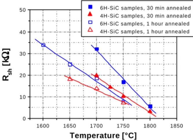
It is also important to note that the roughness of the sample surfaces after annealing increases with the temperature and the annealing time, this process becomes excessive for temperatures and times superior to 1700°C and 30 min. 1600 1650 1700 1750 1800 1850 0 10 20 30 40 50 Temperature [°C] R sh [kΩΩ ]
6H-SiC samples, 30 min annealed 4H-SiC samples, 30 min annealed 6H-SiC samples, 1 hour annealed 4H-SiC samples, 1 hour annealed
Fig. 4: Sheet resistance variations with annealing temperature for 30 min and 1 h annealing duration, measured at RT by four-point probe technique.
Electrical activation of dopants on implanted and annealed samples was investigated by Rsh measurements with a four-point probe technique. Rsh decreases when the annealing temperature or the annealing time increases. In Fig. 4 Rsh variations with the annealing temperature are represented, for 30 min and 1 hour annealing times. The weaker values for the sheet resistance on the 4H-SiC are mainly the consequence of weaker ionization energy of the Al dopants in 4H-SiC rather than a better electrical activation after high temperature annealing [5]. The linearity of the Rsh variations proves a non saturation of electrical dopant activation, nevertheless regression lines intersect temperature axe between 1800°C and 1820°C for the 4H-SiC and 6H-SiC samples, which
illustrates that these annealing conditions lead to nearly complete Al dopant activation.
Rsh measurements made on VdP or TLM structures of SiC wafers show a linear dependence with the distance between the tested structure and the center of the wafer. Figure 5 presents results obtained on the 4H-SiC wafer. Similar results were found on the 6H-SiC samples. Sheet resistance found by TLM measurements must be corrected by a geometrical factor.
0 3 0 0 0 6 0 0 0 9 0 0 0 1 2 0 0 0 1 5 0 0 0 1 0 1 2 1 4 1 6 1 8 2 0 structure-to-center distance [µm] (a) Rsh [k ΩΩ ] R s h o n V d P s t r u c t u r e s R s h o n T L M s t r u c t u r e s 0 3000 6000 9000 12000 15000 3x10¹⁷ 4x10¹⁷ 5x10¹⁷ 6x10¹⁷ 7x10¹⁷ structure-to-center distance [µm] (b) Hall concentration [cm -3 ] (c) VDP TLM
Fig. 5: Sheet resistance measured on VdP and TLM structures (a) and hall concentration variation (b) on a 4H-SiC wafer annealed at 1700°C during 30 min. Top mask view of VdP and TLM structures (c)
A good agreement is found between the sheet resistance measured on the VdP structure placed at the wafer center (19.2 kΩ in Fig. 5a) and the values obtained by four point probe technique on 5×5 mm2 whole surface implanted samples, annealed in the susceptor center (19.7 kΩ in Fig. 4). The linear variations of Rsh on VdP wafer structures compared with the results presented in Fig. 4, i.e. the linear relationship between Rsh and the annealing temperature, involve an almost linear temperature variation at the surface of the susceptor, due to the induction heating system. The temperature increases from the center of the susceptor to its periphery. The difference of 30°C between the center and the wafer periphery, evaluated by fitting Rsh linear variation with the temperature (Fig. 4) and the Rsh measured on VdP structures (Fig. 5a), is in agreement with thermodynamic calculations of the susceptor induction heating process (Fig. 1).
As a consequence and confirmation of this temperature distribution, we observed that the roughness of the wafer increases from the center to the periphery.
SIMS measurements realized locally in p-type implanted regions (VdP structures) show that the dopant profile does not depend on the structure-to-center distance. Therefore the decrease of the sheet resistance from the center to the periphery is attributed to the electrical activation of implanted dopants, which increases following the susceptor temperature variation during the post-implantation annealing process.
A linear variation of the carrier concentration is also determined by Hall effect measurements (Fig. 5b) at room temperature, the mobility values preserving a rather constant value (18 cm2V-1s-1). High values of hall concentration involve a good electrical Al dopant activation.
Conclusion
Aluminum implantation at RT was analyzed in 6H and 4H-SiC using high temperature annealings in an induction heating furnace. Amorphous layers are well recrystallized and no dopant loosing occurs after annealing. Electrical activation of aluminum increases when the annealing temperature or the annealing time increases, complete activation has been found both for 6H and 4H-SiC for annealing at about 1800°C during 30 min. Based on these results and the electrical activation distribution maps on SiC wafers, measured on VdP structures, we have determined the radial temperature gradient to be ~30°C, the periphery being hotter. Radial temperature gradient at the surface of the susceptor induces a better electrical activation of Al-implanted zones annealed at the periphery of the susceptor. To avoid non-uniform temperature effects susceptor has to be remodeled. Otherwise this effect has to be considered in device realization.
Acknowledgements
The authors gratefully thank C. Dubois (from LPM - INSA de Lyon) for SIMS analyses, B. Canut (from DPM - UCB Lyon I) for RBS measurements and CIME (Grenoble) team for technological means availability. DGA and GIRCEP group are thanked a lot as well for interest as for support.
References
[1] M. Lazar, L. Ottaviani, M.L. Locatelli, D. Planson, B. Canut and J.P. Chante: Mater. Sci. Forum Vol. 338-342 (1999), p. 921
[2] N.G. Chechenin, K.K. Bourdelle, A.V. Suvurov and A.X. Kastilio-Vitloch: Nuclear Instruments and Methods in Physics Research Vol. B65 (1992), p. 341
[3] E.Morvan, P. Godignon, J. Montserrat, J. Fernandez, D. Flores, J. Milan and J.P. Chante: Mater. Sci. Engineering B46 (1997), p. 218
[4] K.S.Jones, G.A. Rozgonyi: Extended Defects from Ion Implantation and Annealing, Rapid Thermal Processing Science and Technology, Boston, Academic Press (1993), p. 123
[5] T. Troffer, M. Schadt, T. Frank, H. Itoh, G. Pensl, J. Heindl, H.P. Strunk and M. Maier: Phys. Stat. Sol. (a) 162 (1997), p. 277
![Fig. 3: SIMS analyses in as-implanted and 1700°C during 30 min annealed 6H-SiC samples, compared to I 2 SiC Monte-Carlo simulation [3]](https://thumb-eu.123doks.com/thumbv2/123doknet/14582950.729531/3.894.145.781.740.990/analyses-implanted-annealed-samples-compared-monte-carlo-simulation.webp)