Accurate and Efficient Dynamic Simulations
of Ferroelectric Based Electron Devices
The MIT Faculty has made this article openly available.
Please share
how this access benefits you. Your story matters.
Citation
Rollo, T. et al. "Accurate and Efficient Dynamic Simulations
of Ferroelectric Based Electron Devices." 2019 International
Conference on Simulation of Semiconductor Processes and Devices
(SISPAD), September 2019, Udine, Italy, October 2019. © 2019 IEEE
As Published
http://dx.doi.org/10.1109/sispad.2019.8870373
Publisher
Institute of Electrical and Electronics Engineers (IEEE)
Version
Author's final manuscript
Citable link
https://hdl.handle.net/1721.1/130948
Terms of Use
Creative Commons Attribution-Noncommercial-Share Alike
Accurate and Efficient Dynamic Simulations of
Ferroelectric Based Electron Devices
T. Rollo
(1), L. Daniel
(2), D. Esseni
(1)Email: [email protected]
(1) DPIA, University of Udine, Italy; (2) Electrical Engineering and Computer Science Depart., MIT, Cambridge, MA, USA.
I. INTRODUCTION
In recent years electron devices based on ferroelectric materials have attracted a lot of interest well beyond FeRAM memories. Negative capacitance transistors (NC-FETs) have been investi-gated as steep slope transistors [1], [2], and Ferroelectric FETs (Fe-FETs) are under intense scrutiny also as synaptic devices for neuromorphc computing, where the minor loops in ferroelectrics can allow to achieve multiple values of conductance in read mode [3], [4], [5]. Furthermore, the persistence of ferroelectricity in ultra-thin ferroelectric layers paved the way to ferroelectric tunnelling junctions [6], where a polarization dependent tunneling current can be exploited to realize high impedance memristors, amenable for ultra power-efficient and thus massive parallel computation.
In all the above devices the dynamics of ferroelectric domains must be solved self-consistently with the device electrostatics. Furthermore, in MOS transistors having a semiconductor channel, the semiconductor introduces a strong non linearity in the electro-statics, and consequently in the dynamic equations describing the ferroelectric device evolution. The defects at the interfaces also play an intriguing role in ferroelectric FETs [7], in contrast to the well established and detrimental effects in conventional FETs [8]. Moreover, the presence of different trap levels imply a large range of charging and discharging time constants, possibly very different compared to the ferroelectric time constants.
In this paper we compare different numerical integration meth-ods to achieve an accurate and effective simulation of NC-FETs, where the dynamics is governed by possibly very different time constants for either the ferroelectric or interface traps.
II. MODEL DESCRIPTION AND NUMERICAL ALGORITHMS
In the multi-domain, time-dependent Landau-Khalatnikov Equa-tions (LKE) the description of ferroelectric domains requires the numerical solution of a set of differential equations for the polarization Pi of the i-th domain that read [9], [2]
ρdPi dt = −(aiPi+ biP 3 i + ciPi5) + Vf e,i TF e + kX j (Pj− Pi) (1)
where ρ is a resistivity associated to domain switching, k is a coupling factor between nearest neighbor domains and Vf e,i is
the ferroelectric voltage drop for the i-the domain. The ferroelec-tric parameters were calibrated by comparing to experiments in [10], and the resulting set is [2] a=-9.5×10⁸ m/F, b=2.01×10¹⁰
m5/F/C2, c=5.11×10¹⁰ m9/F/C4.When the ferroelectric is oper-ated at small P (e.g. in NC-FETs), the linear term in Eq. (1)
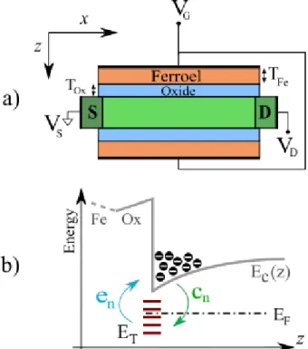
Fig. 1: a) Sketch of the double-gate ferroelectric NC-FET used in our simulations. b) Representation of the capture, cn, and emission, en, processes for electrons at the semiconductor-oxide interface. ET denotes the energy of an individual trap, ECis the conduction band and EF is the local Fermi-level.
is dominant and a time constant τF e=ρ/|a| is readily identified,
which is a property of the ferroelectric material.
Our analysis will be focused on an n-type, double-gate ultra-thin body (DG-UTB), nanoscale NC-FET (see Fig.1(a)), and a single domain analysis is used because the channel length is comparable to the size of ferroelectric domains [11]. Current is calculated with a simple ballistic top-of-the-barrier (ToB) model [12], [13], where electrons at the ToB with positive and negative velocity are taken to be in equilibrium with respectively the source, Ef,S, and drain Fermi level Ef,D=(Ef S-qVDS) [12].
Quantization in the semiconductor is described with a 1D, parabolic effective mass Schr¨odinger solver, with valley multi-plicities, and effective masses corresponding to a [100] silicon interface [14]. The link between the semiconductor and dielectrics is given by continuity conditions for the electric displacement at the interfaces; more modelling details may be found in [15].
We included in our analysis acceptor-type traps in the upper half of the silicon energy gap (see Fig. 1(b)), which exchange electrons with the conduction band with an emission, en, and 978-1-7281-0940-4/19/$31.00 c 2019 IEEE
capture rate cn. The continuity equation for the carrier density
nT in traps with energy ET can be written as [16]
ρ∂nT
∂t = cn(NT − nT) − ennT (2) where NT is the trap density at energy ET, and
en= σ vthNCexp[(ET − EC)/(KBT )] (3a)
cn= σ vthNCexp[(Ef− EC)/(KBT )] (3b)
with EC and Ef being the conduction band edge and local
Fermi level, and σ, vth, NCdenoting respectively the trap
cross-section, thermal velocity and conduction band effective density of states. For any trap energy ET, we solve Eq. (2) self-consistently
with the ferroelectric dynamics governed by Eq. (1), in fact the charge in the traps Qit=−qPETnT(ET) influences the overall electrostatics in the gate stack and thus across the ferroelectric.
Fig. 2: Estimated time constants for the ferroelectric dynamic τF e=ρ/|a|, and for the emission, τe=1/en, and capture process, τc=1/cn, at the silicon oxide interface. In this work we use σ=10−15cm2, vth=2.3 · 107 cm/s, NC=3.2 · 1019cm−3, which are the values experimentally extracted values for a Si-SiO2 interface [17]. Moreover, for the ferroelectric we calibrated the model against data for large area metal-ferroelectric-metal structures [10][15].
Fig. 2 shows the time constant of the ferroelectric, whose parameters were extracted in [15] by comparison to experiments in [10]. Fig. 2 further compares those time constants to those of the interface traps, that depend on the external bias through the alignment between EC and Ef. The figure confirms that a
wide range of time constants are present in the problem at study. In other words the problem is numerically extremely stiff. In the numerical simulation community it is well known that, for such a problem, using standard explicit integrators would force very small time steps in order to avoid numerical instability. Fortunately an efficient implementation, not requiring small time steps and guaranteeing numerical stability, can still be obtained by employing implicit time domain integrators [18], [19], such as the trapezoidal method.
III. RESULTS ANDDISCUSSION
Our results were obtained for an n-type, DG-UTB NC-FET illustrated in Fig.1(a), having a 7 nm silicon film thickness, and a ferroelectric and interfacial SiO2 layer of respectively TF e=20nm
Fig. 3: Total simulation time (for one period of the input signal and for f =5MHz) versus maximum surface-potential error (i.e. potential at the silicon-SiO2interface) for an explicit Runge Kutta and the implicit trapezoidal methods. The shaded area indicates the typical range of acceptable maximum errors for the surface potential, namely between 10−4and 2×10⁻³V at room temperature. Note that the largest time step before the explicit method becomes unstable corresponds to a very small 0.15mV error.
and Tox=0.5nm. An energetically uniform distribution of acceptor
traps is assumed in the upper half of the energy-gap, with a concentration Dit=1013 cm−2eV−1.
In Fig.3 we compare the performance of an explicit integrator (Runge Kutta) with an implicit integrator (Trapezoidal). The figure shows that the total simulation time decreases in both methods for increasing values of the error, computed as the infinity norm of the semiconductor surface potential ϕ at different time-steps δt:
Error = ||ϕδt− ϕ10f s||∞:= max (|φδt− φ10f st|) (4) where the potential calculated for δt=10fs was used used as the
reference. However Fig.3 also shows that the explicit integrator becomes unstable for time steps larger than those needed to produce an error of 0.2mV. In other words, the explicit method is forced to continue using very small time steps and producing a small error even when larger errors would be acceptable. On the other hand the implicit integrator does not have stability problems, not even when using larger time steps when targeting larger values of the error in exchange for faster simulation times. For instance, if an error of 1mV is considered acceptable by the user, the implicit integrator could solve the problem in just 3 minutes while the explicit integrator would still be forced to require more than 4 hours to solve the problem to avoid numerical instability.
Fig.4 reports the simulated IDS-VG curves for two frequencies
of the triangular gate voltage waveform. A few periods of the VG input waveform were simulated and we verified that the IDS
becomes periodic after the first two or three periods, so that the IDS-VG curve plot can be obtained by taking the corresponding
IDS and VG values in the last period of the VG waveform. The
results obtained with explicit and implicit methods are compared at two time steps, demonstrating a remarkable speed-up of the
Fig. 4: Comparison of IDS-VGcharacteristics at different frequencies and for two integration methods . The curves are obtained with a uniform trap density Dit=1013cm−2/eV , the LKE coefficients reported in fig.2 and for a ρ=0.5Ωm. The curves obtained with the different integration methods are almost indistinguishable, but the speedups are consistent with the ones reported in Fig.3.
Fig. 5: Occupation probability Pt=nt/Ntfor two trap levels (in midgap position and closer to the conduction band) corresponding to the f =500MHz curve in Fig.4 and for three integration time-steps δt; the VGinput waveform is also shown (right y axis).∆ET=EC-ET is the distance between the energy level of the trap and the conduction band at the semiconductor-dielectric interface.
simulation time, enabled by a drastic reduction of the time step for a given accuracy. From a device perspective, Fig.4 also confirms how the presence of acceptor type interface traps can help reduce the subthreshold swing below 60mV/dec in NC-FETs (in contrast to the well-known detrimental effect it has in conventional MOSFETs), essentially because the traps improve the capacitance matching between the ferroelectric and the SiO2-semiconductor stack [15]. However such a benefit
tends to vanish at higher frequencies because the occupation of the traps cannot follow the gate voltage waveform, so that the subthreshold steepness of the IDS-VG curve degrades and the
amplitude of the hysteresis enlarges by increasing the frequency. To highlight the sensitivity of simulation outcomes to integration-step variations, in Fig.5 we have reported the
occupa-Fig. 6: Total simulation time (for one period of the input signal and for f =5MHz) versus the relative error on the current IDSfor the implicit integrator; the reference used to calculate the error is the simulated current at deltat=10fs. We here label as on- and off-state current the IDSat respectively VG=0.25 V and VG=−0.3 V (see also the IDS versus VGcharacteristics in Fig.4.
tion probabilities Pt for two energy levels ET at three different
time-step δt values, only for the trapezoidal integrator. At the
frequency of 500MHz the deepest trap, placed 500meV below the conduction band, is not responding to the input waveform VG, meaning that the emission mechanism is not fast enough to
discharge the level ET: this is again consistent with the behavior
of the IDS-VG characteristics reported in Fig.4 of reference
[15]. Fig.5 also shows that for δt smaller than 10ps the curves
for different δt values are essentially overlapping, whereas for
δt=0.1ns the difference in the Pt waveforms is sizeable. Still
these differences are small and cannot result in an appreciable difference, for example, in the IDS-VG characteristic of the
transistor, such as the curves reported in Fig.4. This is also confirmed by the analysis in Fig.6, where we have reported the relative error for the on- and off-state IDS. As it can be seen for
δt<0.1 ns the IDS difference with respect to the reference value
(i.e. the current calculated for δt=10fs) is smaller than 1%, which
is sufficiently small for most TCAD applications.
IV. CONCLUSIONS
In summary, in this work we systematically demonstrated the advantages of an implicit trapezoidal integrator with respect to a explicit Runge-Kutta method for the simulation of NC-FETs having a wide range of time constants set either by the ferroelectric or by the interface traps dynamics. Advantages are observed in terms of robustness of convergence and in terms of simulation time at fixed accuracy. Our results are expected to be useful in the development of robust TCAD tools for ferroelectric based devices, that are important for the design and optimization of ferroelectric FETs and ferroelectric tunnelling junctions. The growing interest for negative capacitance, steep slope FETs and ferroelectric based synaptic devices for neuromorphc computing will make the modeling and simulation of ferroelectric devices a topic of increasing technological relevance in the near future.
V. ACKNOWLEDGMENTS
The project has received financial support from the MIT International Science and Technology Initiatives (MISTI) Global Seed Funds, within the MIT-FVG Project (University of Udine, Trieste and SISSA).
REFERENCES
[1] S. Salahuddin and S. Datta, “Use of Negative Capacitance to Provide Voltage Amplification for Low Power Nanoscale Devices,” Nano Letters, vol. 8, no. 2, 2008.
[2] T. Rollo and D. Esseni, “New Design Perspective for Ferroelectric NC-FETs,” IEEE Electron Device Letters, vol. 39, no. 4, pp. 603–606, April 2018.
[3] M. Jerry, P.-Y. Chen, J. Zhang, P. Sharma, K. Ni, S. Yu, and S. Datta, “Fer-roelectric FET Analog Synapse for Acceleration of Deep Neural Network Training,” in IEEE IEDM Technical Digest, Dec 2017, pp. 139–142. [4] B. Obradovic, T. Rakshit, R. Hatcher, J. Kittl, R. Sengupta, J. G. Hong, and
M. S. Rodder, “A multi-bit neuromorphic weight cell using ferroelectric fets, suitable for soc integration,” IEEE Journal of the Electron Devices Society, vol. 6, pp. 438–448, 2018.
[5] H. Mulaosmanovic, J. Ocker, S. Mller, M. Noack, J. Mller, P. Polakowski, T. Mikolajick, and S. Slesazeck, “Novel ferroelectric fet based synapse for neuromorphic systems,” in 2017 Symposium on VLSI Technology, June 2017, pp. T176–T177.
[6] B. Max, M. Hoffmann, S. Slesazeck, and T. Mikolajick, “Ferroelectric Tunnel Junctions based on Ferroelectric-Dielectric Hf0.5Zr0.5O2/Al2O3 Capacitor Stacks,” in Proc. European Solid State Device Res. Conf., 2018, pp. 142–145.
[7] T. Rollo and D. Esseni, “Influence of Interface Traps on Ferroelectric NC-FETs,” IEEE Electron Device Letters, vol. 39, no. 7, pp. 1100–1103, 2018. [8] E. H. Nicollian and J. R. Brews, MOS (metal Oxide Semiconductor) Physics
and Technology. Wiley Interscience, 1982.
[9] Z. C. Yuan, S. Rizwan, M. Wong, K. Holland, S. Anderson, T. B. Hook, D. Kienle, S. Gadelrab, P. S. Gudem, and M. Vaidyanathan, “Switching-Speed Limitations of Ferroelectric Negative-Capacitance FETs,” IEEE Transactions on Electron Devices, vol. 63, no. 10, pp. 4046–4052, Oct 2016. [10] D. Zhou, Y. Guan, M. M. Vopson, J. Xu, H. Liang, F. Cao, X. Dong, J. Mueller, and T. S. U. Schroeder, “Electric field and temperature scaling of polarization reversal in silicon doped hafnium oxide ferroelectric thin films,” Acta Materialia, vol. 99, pp. 240–246, 2015.
[11] A. Roelofs, T. Schneller, K. Szot, and R. Waser, “Towards the limit of ferroelectric nanosized grains,” Nanotechnology, vol. 14, pp. 250–253, 2003. [12] A. Rahman, J. Guo, S. Datta, and M.S. Lundstrom, “Theory of Ballistic Nanotransistors,” IEEE Trans. on Electron Devices, vol. 50, no. 9, pp. 1853– 1863, 2003.
[13] S. Rakheja, M.S. Lundstrom, and D. A. Antoniadis, “An Improved Virtual-Source-Based Transport Model for Quasi-Ballistic TransistorsPart I: Cap-turing Effects of Carrier Degeneracy, Drain-Bias Dependence of Gate Capacitance, and Nonlinear Channel-Access Resistance,” IEEE Trans. on Electron Devices, vol. 62, no. 9, pp. 2786–2793, 2015.
[14] D. Esseni, P. Palestri, and L. Selmi, ”Nanoscale MOS Transistors - Semi-Classical Transport and Applications”, 1st ed. Cambridge University Press., 2011.
[15] T. Rollo, H. Wang, G. Han, and D. Esseni, “A simulation based study of NC-FETs design: off-state versus on-state perspective,” in IEEE IEDM Technical Digest, Dec 2018, pp. 213–216.
[16] M.Rudan, Physics of Semiconductor Devices. Springer International Publishing, 2018.
[17] G. Brammertz, K. Martens, S. Sioncke, A. Delabie, M. Caymax, M. Meuris, and M. Heyns, “Characteristic trapping lifetime and capacitance-voltage measurements of GaAs metal-oxide-semiconductor structures,” Applied Physics Letters, vol. 91, p. 133510, 2007.
[18] G. Dahlquist, “A Special Stability Problem for Linear Multistep Methods,” BIT Numerical Mathematics, vol. 3, no. 1, pp. 27–43, Mar 1963. [19] G. Dahlquist and B. Lindberg, “On some implicit one-step methods for stiff
differential equations,” Dept. of Information Processing, Royal Inst. of Tech., Stockholm, Tech. Rep., 1973.
![Fig. 2 shows the time constant of the ferroelectric, whose parameters were extracted in [15] by comparison to experiments in [10]](https://thumb-eu.123doks.com/thumbv2/123doknet/14757635.583340/3.918.74.469.374.689/fig-shows-constant-ferroelectric-parameters-extracted-comparison-experiments.webp)
