HAL Id: hal-02288886
https://hal.archives-ouvertes.fr/hal-02288886
Submitted on 7 May 2020HAL is a multi-disciplinary open access archive for the deposit and dissemination of sci-entific research documents, whether they are pub-lished or not. The documents may come from teaching and research institutions in France or abroad, or from public or private research centers.
L’archive ouverte pluridisciplinaire HAL, est destinée au dépôt et à la diffusion de documents scientifiques de niveau recherche, publiés ou non, émanant des établissements d’enseignement et de recherche français ou étrangers, des laboratoires publics ou privés.
Mapping spin–charge conversion to the band structure
in a topological oxide two-dimensional electron gas
Diogo Vaz, Paul Noël, Annika Johansson, Börge Göbel, Flavio Bruno,
Gyanendra Singh, Siobhan Mckeown-Walker, Felix Trier, Luis Vicente-Arche,
Anke Sander, et al.
To cite this version:
Diogo Vaz, Paul Noël, Annika Johansson, Börge Göbel, Flavio Bruno, et al.. Mapping spin–charge conversion to the band structure in a topological oxide two-dimensional electron gas. Nature Materials, Nature Publishing Group, 2019, �10.1038/s41563-019-0467-4�. �hal-02288886�
1
Mapping spin-charge conversion to the band structure in a topological oxide
1
two-dimensional electron gas
2
Diogo C. Vaz1*, Paul Noël2*, Annika Johansson3,4*, Börge Göbel3*, Flavio Bruno5, Gyanendra Singh6, 3
Siobhan McKeown-Walker5, Felix Trier1, Luis M. Vicente-Arche1, Anke Sander1, Sergio Valencia7,
4
Pierre Bruneel8, Manali Vivek8, Marc Gabay8, Nicolas Bergeal6, Felix Baumberger5, Hanako Okuno9, 5
Agnès Barthélémy1, Albert Fert1, Laurent Vila2♥, Ingrid Mertig4,3, Jean-Philippe Attané2 and 6
Manuel Bibes1♦ 7
8
1
Unité Mixte de Physique CNRS, Thales, Univ. Paris-Sud, Université Paris-Saclay, 91767 Palaiseau (France)
9
2
Univ. Grenoble Alpes, CEA, CNRS, Grenoble INP, INAC-Spintec, 38000 Grenoble (France)
10
3
Max Planck Institute of Microstructure Physics, 06120 Halle (Germany)
11
4
Institute of Physics, Martin Luther University Halle-Wittenberg, 06099 Halle (Germany)
12
5
Department of Quantum Matter Physics, University of Geneva, 24 Quai Ernest Ansermet, 1211 Geneva
13
(Switzerland)
14
6
Laboratoire de Physique et d’Etude des Matériaux, ESPCI Paris, PSL Research University, CNRS, 10 Rue
15
Vauquelin, 75005, Paris (France)
16
7
Helmholtz-Zentrum Berlin für Materialien und Energie, Albert-Einstein-Strasse 15, 12489 Berlin (Germany)
17
8
Laboratoire de Physique des Solides, CNRS, Univ. Paris-Sud, Université Paris-Saclay, 91405 Orsay (France)
18
9
Univ. Grenoble Alpes, CEA, INAC-MEM, 38000 Grenoble (France)
19 20
While classical spintronics has traditionally relied on ferromagnetic metals as spin generators and 21
spin detectors, a new approach called spin-orbitronics exploits the interplay between charge and 22
spin currents enabled by the spin-orbit coupling (SOC) in non-magnetic systems. Efficient spin-charge 23
interconversion can be realized through the direct and inverse Edelstein effects at interfaces where 24
broken inversion symmetry induces a Rashba SOC. Although the simple Rashba picture of split 25
parabolic bands is usually used to interpret such experiments, it fails to explain the largest conversion 26
effects and their relation to the actual electronic structure. Here, we demonstrate a very large spin-27
to-charge conversion effect (inverse Edelstein length λIEE > 20 nm) in an interface-engineered
high-28
carrier-density SrTiO3 two-dimensional electron gas (2DEG) and use angle-resolved photoemission
29
measurements and Boltzmann calculations to map its peculiar gate dependence to the band 30
structure. We show that the conversion process is amplified by enhanced Rashba-like splitting due to 31
orbital mixing, and in the vicinity of avoided band crossings with topologically non-trivial order. Our 32
results indicate that oxide 2DEGs formed by a simple room-temperature sputtering procedure are 33
strong candidates for spin-based information readout in novel memory and transistor designs. At the 34
same time, they confirm the promise of topology as a new ingredient to expand the scope of 35
complex oxides for spintronics. 36
* these authors contributed equally to this work. ♥ [email protected] ♦[email protected]
2
The Rashba effect is a quantum phenomenon that occurs at surfaces and interfaces where spatial 38
symmetry breaking results in an out-of-plane electric field1. In the presence of spin-orbit coupling 39
(SOC), this leads to a lifting of the spin degeneracy and a locking of the momentum and spin degrees 40
of freedom causing pairs of Fermi contours with a momentum splitting and opposite spin chiralities2.
41
When a two-dimensional (2D) charge current flows in a Rashba system, it generates a transverse 42
spin density through the Edelstein effect (EE) (also called Rashba-Edelstein or inverse spin galvanic 43
effect)3. This spin density can diffuse in an adjacent conducting material through the interface, 44
generating a three-dimensional (3D) pure spin current without net charge current (that is, a pure 45
flow of spin angular momentum, with opposite flows for electrons of opposite spins). Conversely, the 46
injection of a spin current into a Rashba system generates a net charge current (inverse Edelstein 47
effect, IEE or spin galvanic effect)4. The EE and IEE can also be realized at surfaces of three-48
dimensional topological insulators5, and have been predicted in other types of quantum materials6,7. 49
The interpretation of the IEE in topological insulators is relatively simple since they usually have only 50
one Fermi contour. The figure of merit = ⁄ is given by the product of the Fermi velocity 51
and the momentum relaxation time (Ref. 8). However, the situation is more complex in Rashba
52
systems, where conversion occurs in two inequivalent Fermi contours whose contributions partially 53
compensate each other4,9, so that = α τ ħ⁄ (in the approximation of circular Fermi contours)
54
with α the Rashba coefficient. Unexpectedly, the largest values (6.4 nm) were not reported for 55
topological insulators but for SrTiO3-based two-dimensional electron gases (2DEGs) with a moderate
56
effective Rashba SOC10. This unconventional result has been ascribed to the long relaxation time and 57
to the multi-orbital nature of the system10,11. However, a detailed understanding is still lacking. 58
A 2DEG at the interface between SrTiO3 (STO) and another perovskite insulator, LaAlO3 (LAO), first
59
discovered by Ohtomo and Hwang in 200412, possesses many interesting attributes including
low-60
temperature superconductivity and a carrier density that is highly tunable by a gate voltage13. While 61
the mechanisms for 2DEG formation remain debated, it is universally found that a thickness of at 62
least four unit cells of LAO is needed for the 2DEG to appear14 (although it can be reduced by metal 63
capping15,16). Beyond this threshold, the properties of the 2DEG vary little with LAO thickness. Very 64
recently, Rödel et al. reported that a 2DEG could also be formed in STO through the deposition of a 65
few Å of Al at room temperature17. This approach has several advantages as it alleviates the need for 66
the high temperature growth of crystalline LAO and allows the modulation of the carrier density over 67
a broader range, through the adjustment of the Al thickness or the use of other metals18. Here, we 68
report a very large inverse Edelstein effect in such Al/STO 2DEGs. The conversion efficiency and its 69
sign strongly depend on the gate voltage, with λIEE reaching values in the range of ±20 nm. We
70
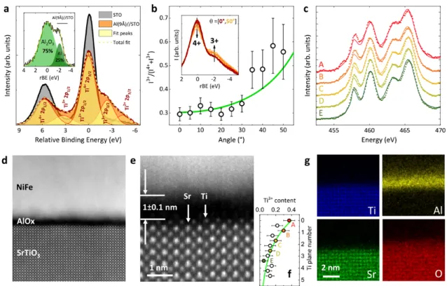
quantitatively relate these values to the Fermi-energy-dependent Edelstein effect calculated within 71
3
the semi-classical Boltzmann transport theory applied to the experimentally determined electronic 72
structure. 73
Following Ref. 17 we prepared STO 2DEGs by depositing an ultra-thin layer of Al (nominal thickness 74
9 Å) on TiO2-terminated STO substrates using magnetron sputtering (see Methods). For scanning
75
transmission electron microscopy (STEM), magnetotransport and spin-pumping experiments, we 76
grew an additional NiFe layer and an AlOx cap (3 nm in thickness) in the same vacuum cycle. The NiFe
77
thickness was 2.5 nm for transport and 20 nm for STEM and spin-pumping. To evaluate the 78
interaction between Al and the first few layers of STO, we performed in situ X-ray photoelectron 79
spectroscopy (XPS) experiments focusing on the Ti 2p and Al 2p states (Fig. 1a). The spectrum 80
collected for a bare STO substrate (grey area) corresponds to a Ti4+ valence state, consistent with its 81
insulating character. Upon deposition of the ultrathin Al layer, two peaks associated with Ti3+ and Ti2+ 82
valence states arise, pointing to the reduction of the STO and the generation of an electron-rich layer 83
at its interface with Al. The spectral weight of these peaks is larger than normally observed in 84
LAO/STO heterostructures16,19, indicating a higher electron density. In the inset, we see that the Al 2p 85
signal comprises two spectral features, corresponding to oxidized and metallic Al (high and low 86
binding energies, respectively) and suggesting that the Al is largely oxidized. As previously reported17, 87
we conclude that Al is able to react with the surface oxygens and thus induces oxygen vacancies 88
acting as electron donors in the first few layers of STO. From here on we thus refer to these samples 89
as AlOx/STO.
90
We have also characterized the interface by cross sectional STEM analysis. As seen in the Z-contrast 91
in high-angle annular dark field (HAADF) images of Figures 1d and 1e, a continuous Al-rich layer can 92
be identified, between the TiO2-terminated SrTiO3 surface and the NiFe layer, with a uniform
93
thickness over all observed areas in the STEM specimen. The AlOx thickness estimated using HAADF Z
94
contrast is 1.0±0.1 nm, consistent with the deposition of 0.9 nm of Al metal and its volume expansion 95
upon oxidation. Sr, Ti, Al and O elemental chemical maps have been acquired using electron 96
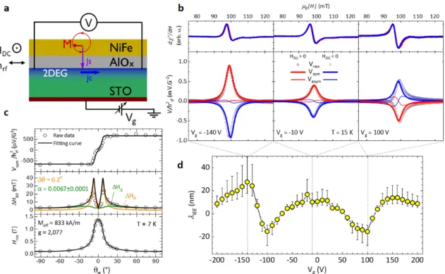
dispersive X-ray spectroscopy (EDX), and show that oxygen is present in STO but also extends 97
through the Al layer. A tiny amount of Ti also appears to be present in the Al-rich region. Overall, the 98
STEM analysis corroborates the XPS data and clearly evidences that the Al layer is oxidized at the STO 99
interface. 100
To estimate the spatial distribution of the Ti3+-rich layer, we performed angle-dependent XPS 101
experiments (cf. Fig. 1b) and electron energy loss spectroscopy (EELS) at the Ti L3,2 edge (cf. Fig. 1c).
102
EELS data in the Al-rich region (see Supplementary Material) suggest that most of the Ti2+ seen in XPS 103
is found within the Al-rich layer. In Fig. 1b, we plot the ratio between the weights of the Ti3+ and Ti4+ 104
4
peaks, that increases exponentially with the XPS electron take-off angle, indicating a larger 105
concentration of Ti3+ closer to the interface. The data are well fitted using a depth-profile model, 106
previously used to estimate the thickness of 2DEG in LAO/STO samples19. We extract a total electron 107
density of 7.2±1.0×1014 cm-2 and a thickness of 1.4±0.4 nm, confirming the quasi 2D nature of the 108
electron gas. The mixed valence of Ti in STO is also seen in the EELS data presented in Fig. 1c, that we 109
simulated with linear combinations of Ti3+ and Ti4+ reference signals (taking into account the 110
experimental resolution). The extracted Ti3+ content is plotted in Fig. 1f, and is found to decrease
111
when going deeper into the STO. The total Ti3+ concentration corresponds to an electron density of 112
6.3±1.0×1014 cm-2, consistent with the XPS analysis. 113
114
Figure 1. Characterization of AlOx/STO 2DEGs. (a). X-ray photoelectron spectra near the Ti 2p state 115
for a STO single crystal before (black) and after (red) deposition of 9 Å of Al. Inset: spectrum at the Al 116
2p state after deposition of 9 Å of Al on STO; rBE stands for relative binding energy. (b) Ti3+ fraction 117
for different take-off angles. The error bars come from the fitting process using CasaXPS (see 118
Methods). The experimental spectra are shown in the inset. The green line is a fit using the model of 119
Ref. 19. (c) EELS spectra at positions indicated in (f) in SrTiO
3 (dotted) with simulations (lines) using
120
linear combinations of Ti3+ and Ti4+ spectra corrected for instrumental resolution. (d) Scanning 121
transmission electron microscopy image. (e) Magnified view of (d). (f) Variation of the Ti3+ content 122
deduced from simulations shown in (c) as a function of position in SrTiO3. The green line is an
123
exponential fit. (g) EDX maps. 124
5
We now turn to the transport properties. The temperature dependence of the sheet resistance for a 125
AlOx/NiFe/AlOx/STO sample and a AlOx/NiFe/STO reference sample is displayed in Fig. 2a. Without
126
the Al insertion (brown curve), the resistance shows practically no change over the whole range of 127
temperatures. In contrast, in the full stack (black curve) a drop in resistance is observed below 100 K, 128
signalling an additional conduction path corresponding to the 2DEG. The red curve represents the 129
isolated 2DEG contribution, deduced through a two-channel parallel conduction model16. Hall traces 130
of the 2DEG were extracted16 from Hall measurements at T = 7 K while applying a back-gate voltage 131
Vg. While a non-linear Hall signal was obtained for large positive gate voltages, decreasing Vg
132
promoted a more linear dependence, suggesting that a transition between multi-band and single-133
band transport occurs. Fitting the Hall traces in the linear regime and using capacitance 134
measurements20 we obtained the mobile carrier densities in both regimes. As visible in Fig. 2b, the
135
carrier density varies from about 7×1013 cm-2 at -175 V to 1×1014 cm-2 at +175 V. We note that, as
136
often reported in STO 2DEGs, the density of mobile carriers is significantly lower than the total 137
electron concentration inferred from core level spectroscopy19, suggesting the existence of a large
138
fraction of localized electrons. 139
140
Figure 2. Magnetotransport properties. (a) Temperature dependence of the sheet resistance of a
141
AlOx/NiFe/AlOx/STO sample (black) and a AlOx/NiFe/STO reference sample, with a deposited Al
6
thickness of 9 Å (brown). The extracted contribution from the 2DEG is shown in red. (b) Carrier density 143
as a function of gate voltage. The shaded area, derived from the capacitance measurement, 144
corresponds to the uncertainty in the determination of nHall.
145
To characterize the IEE in our AlOx/STO 2DEGs, we used spin pumping ferromagnetic resonance
146
(FMR) experiments at 15 K on a AlOx/NiFe(20 nm)/AlOx/STO sample with a nominal deposited Al
147
thickness of 9 Å (see Methods). Fig. 3a depicts the principle of the technique: DC and radio frequency 148
(rf) magnetic fields HDC and hrf are applied to excite magnetization precession in the NiFe layer. At
149
ferromagnetic resonance, a pure spin current is injected in the 2DEG21. In the presence of IEE, a
150
transverse DC voltage will be generated. Fig. 3b shows FMR signals (top panels) at different gate 151
voltages. The FMR resonance field and the linewidth do not vary, implying that the gate voltage does 152
not affect the properties of the ferromagnet. The bottom panels of Fig. 3b show the voltage signals 153
produced at resonance, possessing two components: a symmetric one and a much smaller 154
antisymmetric one (Vsym and Vasym, respectively), both of which are reversed upon reversing HDC.
155
While the antisymmetric component arises from spin rectification effects such as anisotropic 156
magnetoresistance, the symmetric component (spin signal) is due to spin-charge conversion (by 157
inverse spin Hall effect – ISHE – or IEE). For all gate voltages shown, Vsym strongly dominates the
158
signal, pointing to a high spin-charge conversion efficiency. In addition, the signal was observed to be 159
linear with the rf power, for a maximum of 5 mW. 160
161
Figure 3. Spin-charge conversion in NiFe/AlOx/STO. (a) Sketch of the spin pumping experiment. (b) 162
FMR curves (top) and spin signals (bottom) for different values of the gate voltage, for a positive (red) 163
7
and negative (blue) applied DC magnetic field. The symmetric Vsym and antisymmetric Vasym
164
components of the raw spin signals Vraw are represented using continuous thick and thin lines,
165
respectively. (c) Top panel: angular out-of-plane dependence of the amplitude of the symmetric 166
component of the spin-pumping signal, normalized by the square of the applied rf field. Center panel: 167
angular out-of-plane dependence of the ferromagnetic resonance peak-to-peak linewidth. The fit 168
enables the separation of the contributions of the damping (ΔHG) and the magnetic inhomogeneities
169
in the FM layer (ΔHθ), thus allowing the extraction of the damping parameter α. Bottom panel: 170
angular out-of-plane dependence of the ferromagnetic resonance field. The fit allows the extraction 171
of the magnetization and g-factor. All the fits have been made using the model proposed in Ref.22 (d) 172
Spin-charge conversion efficiency λIEE as a function of gate voltage at 15 K. The error bars come from
173
the uncertainty in the determination of the spin mixing conductance (see Supplementary Material). 174
The out-of-plane angular dependence of the spin signal amplitude, shown in Fig. 3c, is in agreement 175
with the theoretical expectations for ISHE or IEE22. The out-of-plane angular dependences of the 176
ferromagnetic resonance peak-to-peak linewidth ΔHpp and the ferromagnetic resonance field Hres
177
allow the extraction of the magnetization Meff=833 kA.m-1, the g-factor g=2.077 and the damping
178
α=0.0066 that are typical of a 20 nm thick NiFe film. 179
The value of can then be calculated by comparing the value of α with that of a reference NiFe/Si 180
sample21; the spin mixing conductance was ↑↓ =2.2±1 nm-2 (see Supplementary Material). can 181
be extracted from the spin signal value and the sample resistivity4. From and we calculate 182
and plot its gate dependence in Fig. 3d. The spin-charge conversion varies strongly in sign and 183
amplitude, with its sign changing several times in the studied range of gate voltages. Moreover, the 184
conversion efficiencies at maximum values are extremely high, for both positive and negative values 185
(+28 nm, -16 nm). These efficiencies are, in absolute value, much higher than those measured in 186
other spin-orbit systems. In spin Hall materials, can be compared to the product of the spin Hall 187
angle and the spin diffusion length, and typical values are below 1 nm for Pt or W23. In topological 188
insulators, values go up to 2.1 nm in α-Sn (Ref. 5), 2.0 nm in HgTe (Ref. 24), and 0.08 nm in (Bi, 189
Sb)Te (Ref. 25). The conversion efficiency observed here is also higher than what can be obtained in
190
Rashba interfaces (0.3 nm in Ag/Bi, Ref. 4), or even in previously studied oxide-based systems (6.4 nm 191
in LAO/STO, Ref. 10, and 0.6 nm in Cu/Bi2O3, Ref.26).
192
To gain more insight into the relationship between the IEE effect and the electronic structure of STO 193
2DEGs, we have performed angle-resolved photoemission experiments on Al/STO and vacuum-194
cleaved STO samples with integrated carrier densities in the 1013-1014 cm-2 range (see Supplementary 195
Material). Fig. 4a displays the ARPES Fermi surface of a 2DEG stabilized at the (001) surface of STO for 196
8
a sample with n≈1.5×1014 cm-2. In bulk STO, dxy, dyz, and dzx bands near the Fermi energy are
197
hybridized due to spin-orbit interaction. The confinement in the 2DEG leads to the creation of sub-198
bands and the emergence of an unconventional Rashba effect with a spin splitting that is enhanced 199
in certain k-space areas27–29 due to orbital mixing. We resolve three concentric circular contours 200
centred at the Γ11 point and two ellipsoidal Fermi surface sheets with major axes along the kx and ky
201
direction, respectively, giving four inequivalent bands in total (two heavy and two light bands), 202
consistent with previous studies17,27,30. The ellipsoidal features have lower intensity due to the light
203
polarization chosen for this experiment27. Electronic structure dispersion plots along the high 204
symmetry directions Γ-X [100] and Γ-M [110] are displayed in Figures 4b and 4c respectively. In the 205
dispersion plot along Δ, shown in Figure 4d, we resolve the lowest lying sub-band that forms the 206
outer Fermi surface sheet. In addition, we observe additional spectral weight at kΔ=0 located ∼15
207
meV below the Fermi level (see Supplementary Material). 208
9
Figure 4. Electronic and spin structure of the 2DEG. (a) Experimental Fermi surface of the 2DEG
210
around the Γ11 point. (b) Band dispersion along the [100] direction − cf. cyan dashed line in (a), with
211
overlaid bands calculated by an eight-band tight-bonding model. (c) Same along the [110] direction − 212
cf. yellow dashed line in (a). The insets to (a,b) use an enhanced contrast to better visualize the faint 213
heavy bands (see Methods). (d) Same along the Δ direction – cf. green dashed line in (a). (e) 214
Calculated band structure along Δ near kc. (f) Calculated Fermi surface and spin expectation values
215
(direction: arrows, absolute value: color scale) at an energy near the band inversion region, where the 216
left (right) panel corresponds to the outer (inner) band of each pair. The numbers denote the band in 217
energetically ascending order. (g) is a zoom-in near kc (boxed region in f).
218
Next, we derive a model Hamiltonian that reproduces the ARPES measurements. We take into 219
account the two energetically lowest dxy bands and one dyz and dzx band, respectively. Accounting for
220
spin, this results in an eight-band effective Hamiltonian (see Methods), which reproduces the 221
measured ARPES band structure very well (Fig. 4a-d). Fig. 4e shows the calculated band structure 222
along a Δ direction (perpendicular to the [110] direction). Because of the interplay between spin-223
orbit coupling and orbital mixing, the band structure shows a band inversion with an avoided 224
crossing at the critical k point kc (corresponding to kΔ=0). This band inversion renders the 2DEG
225
topologically non-trivial and gives rise to spin-polarized topological edge states that have been 226
predicted in Ref.31 by means of the Z2 topological invariant. Figs. 4f and 4g show the spin expectation
227
value for all eight bands. The band inversion discussed in Fig. 4d and 4e leads to strong modulations 228
of the spin expectation values near the Fermi energy. Indeed, as observed in Fig. 4g, the spin 229
expectation value almost vanishes in the fourth band near kc, while it remains considerable in the
230
third band, leading to uncompensated spin textures. 231
Let us now examine how this peculiar band structure produces spin-charge interconversion. We 232
characterize the direct Edelstein effect efficiency by the tensor that relates the spin per surface 233
unit cell to the externally applied electric field , = . In Fig. 5b, we plot the direct Edelstein 234
efficiency calculated from the spin expectation values for different Fermi energies (assuming a 235
rigid band shift) using a semi-classical Boltzmann approach (see Methods). Since the EE is the 236
Onsager reciprocal of the inverse Edelstein effect9 (in the approximation of transparent interfaces),
237
the experimental data of Fig. 3d (that we replot in Fig. 5a) can be compared with the theoretical 238
results. At low energy, only the two low-lying dxy sub-bands ( in Fig. 5c) are occupied and is
239
relatively small, consistent with the modest Rashba-like splitting of these bands. Upon increasing 240
energy, a step occurs corresponding to the population of the next dxy sub-band pair () followed by
241
an extremum signaling the onset of the first heavy sub-band pair (). Then, decreases and 242
10
changes sign, owing to the alternating sign of the spin splitting between the dxy and the first pair of
243
dzx,yz bands29,32 (as discussed in Ref.11), reaching a large negative value corresponding to the trivial
244
avoided crossing (), i.e. the first crossing between light dxy and heavy dzx,yz bands where orbital
245
mixing enhances Rashba splitting27. Another extremum followed by a slope change of occurs at
246
the band edge of the second pair of dzx,yz bands, again due to opposite spin splitting compared to the
247
fifth and sixth bands (), as seen in the light blue curve of Fig. 5b (top panel). Upon further 248
increasing energy, the topological band inversion is reached () where the uncompensated spin 249
texture between the third and fourth bands causes a pronounced maximum in the Edelstein signal. 250
This large spin-charge conversion efficiency is a consequence of the topological order in the system. 251
We point out, however, that it is not caused by topological edge states themselves, whose 252
contributions would compensate at opposite edges of the 2DEG. 253
11
Figure 5. Energy dependence of the spin-charge conversion. (a) Gate dependence of at 15 K. (b) 255
Energy dependence of the Edelstein tensor (top: band-resolved; bottom: total). (c) Fermi lines at 256
various energies. Rashba-like bands 1+2. Edge of bands 3+4. Edge of bands 5+6. Trivial 257
avoided crossing. Edge of bands 7+8. Topologically non-trivial avoided crossing (with band 258
inversion). Maximum from multiple bands. The colour scale of the zoom-in regions in and 259
corresponds to the contribution of each state to the Edelstein effect. 260
While the trivial avoided crossing in the [100] direction () unlocks only an enhanced Rashba spin 261
splitting due to orbital mixing, the topologically non-trivial avoided crossing in the Δ direction adds a 262
large contribution from the uncompensated spin texture (see both insets of Fig. 5c), which drives the 263
overall Edelstein effect to large values in this region. This can be better understood by recalling the 264
nature of the Edelstein effect in a Rashba system, where the net spin-charge current produced arises 265
from the inequivalence of the Fermi contours. If the spin splitting between bands is larger, i.e. if 266
Fermi contours have very different sizes, this inequivalence is enhanced. A similar result is intuitively 267
obtained if the spin-split bands have uncompensated spin textures, where the spin current produced 268
through the EE by one contour would be much larger than the one produced by its Rashba-split 269
counterpart. Lastly, for even higher energy, another sign change occurs followed by a negative 270
extremum, resulting from the competing contributions from multiple bands (). 271
Remarkably, the calculated curve qualitatively reproduces the occurrence of extrema and sign 272
changes in the IEE signal. However, the presented energy range cannot be unambiguously related to 273
the depicted gate voltage. To gain more insight into their correspondence, we have performed 274
Poisson-Schrödinger calculations of the energy spectrum for an STO interface (see Supplementary 275
Material). They indicate that to shift the Fermi level from the expected energy of the topologically 276
avoided crossing to the trivial avoided crossing, the 2DEG needs to be depleted by Δn=2.6×1013 cm-2. 277
By matching these two points in Fig. 5c ( and ) with points D and C in Fig. 5a, we observe that VG
278
was swept between about 0-20 V and -100 V, respectively. According to the transport data in Fig. 2b, 279
this range of gate voltages is equivalent to a depletion of Δn=1.7±1×1013 cm-2, compatible with the 280
estimation from Poisson-Schrödinger calculations. 281
Although the energy dependence of and are quite comparable and can be related to the 282
spin splittings of the band structure of the AlOx/STO 2DEG, the explanation of the extremely large IEE
283
signal needs another ingredient. In the theoretical description scattering is restricted to the 2DEG 284
only. In the experiments, however, the electrons have in principle the possibility to leak out of the 285
2DEG through a tunneling barrier (in this case, the AlOx layer), and scatter in the metal with very
286
short relaxation times (typically tens of fs). This can be considered as a second scattering channel33,34 287
12
characterized by an escape time τesc through the tunneling barrier, in addition to the scattering
288
between the STO states with characteristic time τ2DEG. The two scattering channels lead to an
289
effective relaxation time τeff=(τ2DEG-1 + τesc-1)-1 that will set the efficiency of the conversion process.
290
The strength of this second scattering channel can modify the IEE signal considerably. Long escape 291
times would change the IEE signal only slightly and result in an optimal spin-charge conversion signal, 292
while short escape times, as in metallic interfaces such as Ag/Bi4, would considerably reduce τeff and
293
consequently the IEE signal. We can use this picture to compare the values of found in 294
NiFe/LAO//STO samples10 and here in NiFe/AlO
x//STO. We deduce the escape times through 2 uc
295
LAO and ∼1 nm of AlOx from their estimated resistance area (RA) product (through = ∗ ℏ
296
with RA≈10 Ω.µm² and 105Ω.µm², respectively). This leads to escape times in the ps range for 2 uc 297
of LAO and in the 10 ns range for 1 nm of AlOx. We see that for 2 uc of LAO τesc is comparable to or
298
shorter than the momentum relaxation of the 2DEG τ2DEG, estimated to 1-10 ps, which should lead to
299
a reduction of compared to an isolated 2DEG. On the other hand, for the present NiFe/AlOx/STO
300
samples, τesc is much longer than τ2DEG: the electrons will scatter within the 2DEG before having a
301
chance to leak out to the metal. In this case, the 2DEG is well isolated from the metal by the alumina 302
barrier, and can approach its optimum value. 303
Finally, to evaluate the application potential of our system, we have performed spin pumping 304
experiments to determine the expected output voltage at room temperature. This quantity, given by 305
the product of and the sheet resistance, is the figure of merit for devices and is relevant for 306
instance for the spin transistor proposed by Intel (MESO device)36. Since is proportional to the 307
momentum relaxation time (and thus to the electron mobility) one expects a strong decrease of 308
upon increasing the temperature, but in parallel the sheet resistivity should increase correspondingly 309
and largely compensate this decrease. For the present heterostructure we find a considerable 310
=0.5±0.1 nm at room temperature, and a sheet resistance on the order of 2.5 kΩ. The output 311
voltage in the MESO device can be calculated from 312
=
with the spin polarization, the supply current density and the device width. Taking 313
= 0.5, = 5×10¹⁰ A/m² and = 300 nm, we obtain ≈ 10 mV, just one order of
314
magnitude lower than the targeted value of 100 mV. This has to be compared with the value of 315
one can estimate for a Pt film of 5 nm in thickness ( ), that would have = / =20 Ω and an 316
equivalent = with = 0.06 the (inverse) spin Hall angle and = 4 nm the spin 317
diffusion length, leading to = 0.2 nm. This yields = 0.03 mV, i.e. two to three orders of 318
magnitude less than with our STO 2DEG. 319
13
In summary, we have reported spin-charge conversion in an oxide 2DEG formed by the room-320
temperature sputtering deposition of Al on SrTiO3, with an efficiency about two orders of magnitude
321
larger than that of the canonical spin-orbit coupling material, Pt. We have related the amplitude of 322
the effect and its strong gate dependence to the band structure of the 2DEG, possessing trivial and 323
topological avoided crossings, and to the high tunnel resistance of the Al oxide layer. Highly-doped 324
STO-based oxide interfaces thus emerge as new members of the family of topological two-325
dimensional materials, able to realize specific functions for spintronics devices. Our observation of a 326
finite spin-charge conversion effect at room temperature, combined with the high resistance of the 327
2DEG and the scalable room-temperature preparation process qualifies STO interfaces as very 328
promising materials for non-volatile spin logic architectures36,37. More fundamentally, our results 329
should stimulate the search for topological phenomena in other oxide 2DEGs38 and interfaces based
330
on elements heavier than Ti that could produce even stronger spin-charge interconversion effects 331
and possibly harbour more exotic states of matter39. 332
333
ACKNOWLEDGMENTS
334
This work received support from the ERC Consolidator Grant #615759 ‘‘MINT’’, the QUANTERA 335
project “QUANTOX”, the French ANR programme through projects OISO (ANR-17-CE24-0026-03), 336
TOPRISE (ANR-16-CE24-0017) and the Laboratoire d’Excellence LANEF (ANR-10-LEBX-51-01). MB 337
thanks the Alexander von Humboldt Foundation for supporting his stays at Martin-Luther-Universität 338
Halle. FT acknowledges support by research grant VKR023371 (SPINOX) from VILLUM FONDEN. AJ, 339
BG and IM acknowledge support by Priority Program SPP 1666 and SFB 762 of Deutsche 340
Forschungsgemeinschaft (DFG). DCV thanks the French Ministry of Higher Education and Research 341
and CNRS for financing his PhD thesis. We thank H. Jaffrès for insightful comments on tunnel escape 342
times, M. Sing for his help with XPS analysis and E. Schierle for his assistance with X-ray absorption 343 spectroscopy measurements. 344 345 AUTHOR CONTRIBUTIONS 346
MB proposed and supervised the study with help from LV, J-PA, AB and AF. DCV prepared the 347
samples with the help of FT and LMVA and performed XPS experiments and analysed the data with 348
AS. DCV, GS and NB measured the magnetotransport properties and analysed the results. HO 349
prepared the samples for STEM and EELS and performed the observations and spectroscopy 350
measurements. SV performed the X-ray absorption measurements and analysed the data. SMW, FYB 351
14
and FB performed the ARPES measurements and their analysis. PN performed the spin-pumping 352
experiments and analysed the data with DCV, LV, J-PA and MB. PB, MV and MG conducted the 353
Poisson-Schrödinger calculations. AJ and BG performed the tight-binding and Boltzmann calculations 354
under the supervision of IM, with inputs from MV, MG and MB. DCV and MB wrote the manuscript 355
with inputs from all authors. All authors discussed the results and contributed to their interpretation. 356
DATA AND CODE AVAILABILITY STATEMENT
357
The data that support the findings of this study are available from the corresponding author upon 358
reasonable request. The self-written code that generated the data for Figs. 4f,g and 5b,c is available 359
from AJ upon reasonable request. 360
15
METHODS
361
Sample preparation. NiFe and Al films were deposited at room temperature by dc magnetron
362
sputtering on TiO2-terminated (001)-oriented STO substrates (from CrysTec GmbH). TiO2-termination
363
was achieved through a chemical treatment, where the substrate was submerged in a buffered 364
hydrofluoric acid (NH4F-HF 7:1) for 30 s and annealed under a rich oxygen environment at 1000 °C for
365
3 h. Prior to in situ XPS or sputtering procedures, the STO substrate was additionally annealed at 730 366
°C for 2 h under a partial oxygen pressure of 400 mbar. The deposition of the metallic layers was 367
performed under an Ar partial pressure of 4.5 x 10⁻⁴ mbar and a substrate-to-target distance of 7 cm. 368
The deposition rates of the Al ultra-thin layer (0.9 nm) and the NiFe layers (2.5 nm for transport and 369
20 nm for spin pumping experiments) was 0.1 and 0.2 nm/s, under an operating dc current of 30 and 370
80 mA, respectively. Samples used for transport and spin pumping were additionally capped with a 371
2.5 nm layer of Al, which becomes oxidized when exposed to air. 372
X-ray photoemission spectroscopy was performed using a non-monochromatized Mg Kα source (hν =
373
1253.6 eV) on 10 mm x 10 mm STO and Al(0.9nm)/STO samples. Spectra analysis was carried out 374
with the CasaXPS software. From a previous work16, the maximum probing depth for this system is
375
estimated to be ∼5 nm. The error bars displayed in the angle dependence experiments were 376
calculated through the error propagation of Ti3+/(Ti4++Ti3+) spectral areas, obtained individually from 377
Monte Carlo simulations in CasaXPS. 378
Scanning transmission electron microscopy measurements have been carried out using a
Cs-379
corrected FEI Themis at 200 keV. HAADF-STEM images were acquired using a convergence semiangle 380
of 20 mrad and collecting scattering from >65 mrad. Energy dispersive X-ray spectroscopy (EDX) was 381
performed for elemental mapping using a Brucker EDX system consisting of four silicon drift 382
detectors in the Themis microscope. STEM specimens were prepared by the FIB lift-out technique 383
using a FEI dual-beam Strata 400S at 30 kV. EELS measurements were performed at 80 kV using a 384
double-aberration-corrected FEI Titan Ultimate TEM equipped with a high brightness electron source 385
and a Gatan Quantum energy filter equipped with Dual EELS. The probe corrector was used to obtain 386
a beam current of 120 pA while maintaining nanometer resolution. The core loss region was 387
recorded over the range 400–600 eV at a dispersion of 0.1 eV pixel−1. 388
Magnetotransport measurements were performed with a PPMS system from Quantum Design after
389
bonding the samples with Al wires. The electrical contribution coming only from the 2DEG was 390
isolated using the method discussed in Ref.16. The variation of the carrier density is obtained by 391
integrating the gate capacitance Cg(Vg) measured by a standard lock-in technique, over the gate
392
voltage range: = < 0 + ( ) where A is the area of the sample and 393
16
< 0 is matched to the maximum and minimum Hall carrier densities experimentally 394
obtained in the underdoped regime. 395
Spin Pumping. The spin-pumping experiments were carried out using a Bruker ESP300E X-band CW
396
spectrometer at 9.68 GHz, with a loop-gap Bruker ER 4118X-MS5 cavity, and using a microwave 397
power of 5 mW or less to remain in the linear regime. The generated DC voltage was measured using 398
a Keithley 2182A nanovoltmeter. The gate voltage was applied using a Keithley 2400 sourcemeter. 399
The sample was initialized by sweeping the back-gate voltage from +200 V to −200 V, and then back 400
to +200 V, to avoid any hysteretic behavior. The measurement was then performed for different gate 401
voltages, from +200V to -200V. 402
Angle-resolved photoemission. ARPES measurements were performed at the SIS beamline of the
403
Swiss Light Source. A single crystal of SrTiO3 slightly doped with La (0.075 wt%) was used to perform
404
the experiments. The introduction of La as a dopant results in a small residual bulk conductivity that 405
helps to avoid sample charging during the experiment. The crystal was cleaved in situ at the 406
measurement temperature of T = 15 K in a pressure lower than 10-10 mbar. The surface was exposed 407
to synchrotron light of 51 eV in order to saturate the bandwidth of the 2DEG30. After this procedure 408
ARPES measurements were taken using linear horizontal polarized photons with an energy of 51 eV. 409
The combined energy resolution was ∼20 meV. In the insets of Fig. 4 (a,b) we have enhanced the 410
contrast by dividing the data by a smooth function of momentum. We verified that this procedure 411
does not significantly change the position of peaks. 412
Tight-binding model. The Hamiltonian is a generalized version of that from Ref.31 We consider the
413
two energetically lowest dxy bands and one dyz and dzx band, respectively. The Hamiltonian includes
414
spin, nearest-neighbor hopping (quantified by , ), spin-orbit interaction () and orbital mixing 415 ( , ) 416 = 0 0 0 −i 0 0 0 −i − − i − − 0 0
− − −i i i 0 0
0 0 − −i 0
0 0 − −i 0
0 0 − − −i
i i 0 0 − − i
,
with the diagonal elements 417
= 2 2 − cos( ) − cos + ,
17
= 2 1 − cos( ) + 2 1 − cos + , and the orbital mixing term
418
= 2i sin( ). The parameters are:
419
= 0.388 eV, = 0.031 eV,
= −0.205 eV, = −0.105 eV, = −0.0544 eV, = 0.002 eV, = 0.005 eV,
= 1 120eV,
resulting in a good agreement with the ARPES data (Fig. 4a-d). 420
Calculation of the Edelstein effect. The tensor for the Edelstein effect characterizes the spin
421
density per unit cell as a response to an externally applied electric field 422
= .
It is calculated using the semi-classical Boltzmann transport theory, 423
=− ( − F).
Here, is the area of the system, is the area of the surface unit cell, > 0 is the elementary 424
charge, and 〈 〉 is the spin expectation value of the state at wave vector and energy . The sum 425
is over all k points and all bands. The mean free path Λ = is approached by the constant 426
relaxation time approximation = 1 ps. At zero temperature, only states at the Fermi level 427
contribute to the Edelstein effect. 428
For the 2DEG Hamiltonian, symmetry only allows for nonzero tensor elements = − . Thus, an 429
external electric field induces an in-plane spin density perpendicular to the field, as in Rashba 430
systems. 431
Poisson-Schrödinger calculations. The electronic states of the carriers in the 2DEG were determined
432
with the help of the Poisson-Schrödinger algorithm which self-consistently yields the shape of the 433
electrostatic potential at the interface and the sub-band structure. For a set total electric charge 434
density, we solved the Schrödinger equation for a particle in a potential well, using values of the 435
effective masses corresponding to the hopping parameters and introduced in the tight-binding 436
model. We also include the atomic spin-orbit coupling in our computation, described by the 437
18
parameter in the tight-binding Hamiltonian. From the eigenfunctions and eigenenergies of the 438
Schrödinger equation one obtains the density profile and then solving Poisson equation gives the 439
spatial dependence of the electrostatic potential in the material. The procedure is then iterated until 440
self-consistency is achieved. 441
19
REFERENCES
442
1. Bychkov, Y. A. . & Rashba, E. I. Properties of a 2D electron gas with lifted spectral degeneracy. 443
JETP Lett. 39, 78–81 (1984). 444
2. Manchon, A., Koo, H. C., Nitta, J., Frolov, S. M. & Duine, R. A. New perspectives for Rashba 445
spin–orbit coupling. Nature Mater. 14, 871–882 (2015). 446
3. Edelstein, V. M. M. Spin polarization of conduction electrons induced by electric current in 447
two-dimensional asymmetric electron systems. Solid State Commun. 73, 233–235 (1990). 448
4. Rojas-Sánchez, J. C. et al. Spin-to-charge conversion using Rashba coupling at the interface 449
between non-magnetic materials. Nature Commun. 4, 2944 (2013). 450
5. Rojas-Sánchez, J.-C. et al. Spin to Charge Conversion at Room Temperature by Spin Pumping 451
into a New Type of Topological Insulator: α-Sn Films. Phys. Rev. Lett. 116, 096602 (2016). 452
6. Han, W., Otani, Y. & Maekawa, S. Quantum materials for spin and charge conversion. npj 453
Quantum Mater. 3, 27 (2018). 454
7. Johansson, A., Henk, J. & Mertig, I. Edelstein effect in Weyl semimetals. Phys. Rev. B 97, 455
085417 (2018). 456
8. Zhang, S. & Fert, A. Conversion between spin and charge currents with topological insulators. 457
Phys. Rev. B 94, 184423 (2016). 458
9. Shen, K., Vignale, G. & Raimondi, R. Microscopic Theory of the Inverse Edelstein Effect. Phys. 459
Rev. Lett. 112, 096601 (2014). 460
10. Lesne, E. et al. Highly efficient and tunable spin-to-charge conversion through Rashba 461
coupling at oxide interfaces. Nature Mater. 15, 1261–1266 (2016). 462
11. Seibold, G., Caprara, S., Grilli, M. & Raimondi, R. Theory of the Spin Galvanic Effect at Oxide 463
Interfaces. Phys. Rev. Lett. 119, 256801 (2017). 464
12. Ohtomo, A. & Hwang, H. Y. A high-mobility electron gas at the LaAlO3/SrTiO3 heterointerface.
465
Nature 427, 423–6 (2004). 466
13. Caviglia, A. D. et al. Electric field control of the LaAlO3/SrTiO3 interface ground state. Nature
467
456, 624–7 (2008).
468
14. Thiel, S., Hammerl, G., Schmehl, A., Schneider, C. W. & Mannhart, J. Tunable quasi-two-469
dimensional electron gases in oxide heterostructures. Science 313, 1942–1945 (2006). 470
20
15. Lesne, E. et al. Suppression of the critical thickness threshold for conductivity at the 471
LaAlO3/SrTiO3 interface. Nature Commun. 5, 4291 (2014).
472
16. Vaz, D. C. et al. Tuning Up or Down the Critical Thickness in LaAlO3/SrTiO3 through In Situ
473
Deposition of Metal Overlayers. Adv. Mater. 29, 1700486 (2017). 474
17. Rödel, T. C. et al. Universal Fabrication of 2D Electron Systems in Functional Oxides. Adv. 475
Mater. 28, 1976–1980 (2016). 476
18. Posadas, A. B. et al. Scavenging of oxygen from SrTiO3 during oxide thin film deposition and
477
the formation of interfacial 2DEG. J. Appl. Phys. 105302, (2017). 478
19. Sing, M. et al. Profiling the Interface Electron Gas of LaAlO3/SrTiO3 Heterostructures with Hard
479
X-Ray Photoelectron Spectroscopy. Phys. Rev. Lett. 102, 176805 (2009). 480
20. Hurand, S. et al. Field-effect control of superconductivity and Rashba spin-orbit coupling in 481
top-gated LaAlO3/SrTiO3 devices. Sci. Rep. 5, 12751 (2015).
482
21. Tserkovnyak, Y., Brataas, A. & Bauer, G. E. W. Enhanced gilbert damping in thin ferromagnetic 483
films. Phys. Rev. Lett. 88, 117601 (2002). 484
22. Rojas-Sánchez, J.-C. et al. Spin pumping and inverse spin Hall effect in germanium. Phys. Rev. 485
B 88, 064403 (2013). 486
23. Pham, V. T. et al. Ferromagnetic/Nonmagnetic Nanostructures for the Electrical Measurement 487
of the Spin Hall Effect. Nano Lett. 16, 6755–6760 (2016). 488
24. Noel, P. et al. Highly Efficient Spin-to-Charge Current Conversion in Strained HgTe Surface 489
States Protected by a HgCdTe Layer. Phys. Rev. Lett. 120, 167201 (2018). 490
25. Mendes, J. B. S. et al. Dirac-surface-state-dominated spin to charge current conversion in the 491
topological insulator (Bi0.22Sb0.78)2Te3 films at room temperature. Phys. Rev. B 96, 180415
492
(2017). 493
26. Karube, S., Kondou, K. & Otani, Y. Experimental observation of spin-to-charge current 494
conversion at non-magnetic metal/Bi2O3 interfaces. Appl. Phys. Express 9, 033001 (2016).
495
27. King, P. D. C. et al. Quasiparticle dynamics and spin-orbital texture of the SrTiO3
two-496
dimensional electron gas. Nature Commun. 5, 3414 (2014). 497
28. Zhong, Z., Tóth, A. & Held, K. Theory of spin-orbit coupling at LaAlO3/SrTiO3 interfaces and
498
SrTiO3 surfaces. Phys. Rev. B 87, 161102 (2013).
21
29. Khalsa, G. & MacDonald, A. H. Theory of the SrTiO3 surface state two-dimensional electron
500
gas. Phys. Rev. B 86, 125121 (2012). 501
30. McKeown Walker, S. et al. Carrier-Density Control of the SrTiO3 (001) Surface 2D Electron Gas
502
studied by ARPES. Adv. Mater. 27, 3894–3899 (2015). 503
31. Vivek, M., Goerbig, M. O. & Gabay, M. Topological states at the (001) surface of SrTiO3. Phys.
504
Rev. B 95, 165117 (2017). 505
32. Zhong, Z., Tóth, A. & Held, K. Theory of spin-orbit coupling at LaAlO3/SrTiO3 interfaces and
506
SrTiO3 Phys. Rev. B 87, 161102 (2013).
507
33. Kim, J. et al. Evaluation of bulk-interface contributions to Edelstein magnetoresistance at 508
metal/oxide interfaces. Phys. Rev. B 96, 140409 (2017). 509
34. Dey, R., Prasad, N., Register, L. F. & Banerjee, S. K. Conversion of spin current into charge 510
current in a topological insulator: Role of the interface. Phys. Rev. B 97, 174406 (2018). 511
35. Herranz, G. et al. High Mobility in LaAlO3/SrTiO3 Heterostructures: Origin, Dimensionality, and
512
Perspectives. Phys. Rev. Lett. 98, 216803 (2007). 513
36. Manipatruni, S. et al. Scalable energy-efficient magnetoelectric spin–orbit logic. Nature 565, 514
35–42 (2019). 515
37. Manipatruni, S., Nikonov, D. E. & Young, I. A. Beyond CMOS computing with spin and 516
polarization. Nature Phys. 14, 338–343 (2018). 517
38. Varignon, J., Vila, L., Barthélémy, A. & Bibes, M. A new spin for oxide interfaces. Nature Phys. 518
14, 322–325 (2018).
519
39. Xiao, D., Zhu, W., Ran, Y., Nagaosa, N. & Okamoto, S. Interface engineering of quantum Hall 520
effects in digital transition metal oxide heterostructures. Nature Commun. 2, 596 (2011). 521