HAL Id: hal-03066791
https://hal.archives-ouvertes.fr/hal-03066791
Submitted on 15 Dec 2020
HAL is a multi-disciplinary open access
archive for the deposit and dissemination of
sci-entific research documents, whether they are
pub-lished or not. The documents may come from
teaching and research institutions in France or
abroad, or from public or private research centers.
L’archive ouverte pluridisciplinaire HAL, est
destinée au dépôt et à la diffusion de documents
scientifiques de niveau recherche, publiés ou non,
émanant des établissements d’enseignement et de
recherche français ou étrangers, des laboratoires
publics ou privés.
Design and Development of Single-Qubit Ion Trap on
Glass and Si Substrates With RF Analysis and
Performance Benchmarking
Anak Agung Alit Apriyana, Hongyu Li, Peng Zhao, Jing Tao, Yu Dian Lim,
Ye Lin, Luca Guidoni, Chuan Seng Tan
To cite this version:
Anak Agung Alit Apriyana, Hongyu Li, Peng Zhao, Jing Tao, Yu Dian Lim, et al.. Design and
Develop-ment of Single-Qubit Ion Trap on Glass and Si Substrates With RF Analysis and Performance
Bench-marking. IEEE Transactions on Components, Packaging and Manufacturing Technology, Institute
of Electrical and Electronics Engineers, 2020, 10 (7), pp.1221-1231. �10.1109/TCPMT.2020.2995388�.
�hal-03066791�
Abstract—This study presents the design and development of
surface electrode ion traps on glass and Si substrate, as well as their RF characterizations and performance benchmarking. In this case, ion-trap on-glass shows superior performances in all necessary criteria. In terms of RF characterizations, ion-traps on glass have Q factor of greater than 900. This is significantly higher than the Q factor of its silicon counterparts, which are around 20 – 300. Such a high Q factor results in power spectral density (PSD) of greater than 10W/MHz. On the other hand, ion-traps on-silicon produce PSD values of lower than 3W/MHz. In terms of RF performance, ion-trap on-glass shows insertion loss lower than 0.2 dB at 60MHz. This is more superior to insertion loss values of ion-traps on-silicon, which are around 1 – 4 dB. The ion-traps metallization is developed using three metallization layers (0.1µm Ti barrier layer, 2.5 – 3.7µm Cu, and 0.3µm Au) on top of dielectric. The on-chip resonance condition can be maintained upon the packaging integration. The laser optical set-up for ion-trapping is verified to capture single 88Sr+ ion.
Index Terms—Ion-trap, power spectral density, power
dissipation, RF analysis, microfabrication, IC packaging, laser excitation, qubit operation
I. INTRODUCTION
UANTUM computing is the computation systems that use quantum-mechanical phenomena (e.g. superposition, entanglement) to perform the computing operation, instead of the conventional Boolean logic by its classical computing counterparts. Quantum computation uses quantum bits, i.e. qubits, to represent ‘1’ and ‘0’ states simultaneously, solving large-scale computation (i.e., chemical simulation, large number factoring and travel salesman problem), which are intractable for classical computer [1]. Superconducting loops, trapped ion, polarized photon, quantum dot and spinning atom can be used as physical implementations for
This document is submitted on 30 May 2019. The work was supported by A*STAR Quantum Technology for Engineering (A1685b0005).
*The first four authors contributed equally to this work.
A.A.A Apriyana, P. Zhao, J. Tao, Y. D. Lim, Y. Lin and C. S. Tan are with Nanyang Technological University, 50 Nanyang Avenue Singapore 639798. (E-mail: aapriyana@ntu.edu.sg, zhao0275@e.ntu.edu.sg, taojing@ntu.edu.sg, yudian.lim@ntu.edu.sg and tancs@ntu.edu.sg).
H. Y. Li is with Institute of Microelectronics, Agency for Science, Technology and Research (A*STAR), Singapore 117685. (email: lihy@ime.a-star.edu.sg)
L. Guidoni is with Laboratoire Matériaux et Phénomènes Quantiques (MPQ), Université Paris, France F-75205 (email: luca.guidoni@univ-paris-diderot.fr).
qubit. Qubit that is based on trapped ion receives more attention recently due to its high efficiency and feasibility of large-scale planar ion-trap electrodes implementation using microfabrication process. With the combination of electric field (E-field) induced by co-planar radio frequency (RF) and direct current (DC) electrodes placed on the same plane, a localized minimum potential point will be formed above the surface, where ion will be trapped. Lasers with specific wavelengths will be exerted onto ions for cooling, state readout and manipulation.
Two states (ground state and excited state) of the valence energy levels in the trapped ions are used to represent logic ‘0’ and ‘1’ of the qubit. Qubit operation can be performed to the trapped ions using a series of laser excitations to induce the laser-atom interactions for inter-state electrons transitions from the ground state to the excited state. When an electron in the ground state (logic ‘0’) is excited with an appropriate laser wavelength, the electron can be excited to higher energy level (logic ‘1’). For logic ‘1’ to logic ‘0’ transition, another laser beam will be required to further excite the electron into the transition states that will spontaneously decay back into the ground state. Depending on the ion lifetime, multiple cycles of this electron transition can be repeated to perform the quantum gate operations [1].
In surface electrode ion-trap design, the typical ‘five-wire’ geometry (control, RF, ground, RF and control) is employed, which consists of two parallel RF electrodes and one ground electrode sandwiched in between forming RF-G-RF lines. Segmented DC electrodes are placed next to each RF electrode, to control the ions position along axial (Z) direction and shuttle ions to certain sites (if necessary), as shown in Fig.1. Ion trap requires RF sources for E-field excitation, and the excited E-field will form the pseudopotential for ion trapping. The ion trapping performance is influenced by the strength of the applied E-field, where stronger E-field produces higher trapping potential, resulting in higherstability of the trapped ion.
Glass has been reported as a candidate substrate for the development of surface electrode ion-trap due to its excellent electrical properties including ultra-high substrate resistivity, low dielectric constant, and ultra-low electrical loss. These properties result in efficient current-to-E-field conversion for the formation of ion-trapping pseudopotential. Efficient current-to-E-field conversion is also crucial in preventing heat generation under the application of RF potential, where the conventional magnitude of RF voltage required for ion trapping can be as high as 100 – 500Vpp. On the other hand,
Anak Agung Alit Apriyana*, Member, IEEE, Hong Yu Li*, Peng Zhao*, Jing Tao*, Yu Dian Lim,
Ye Lin, Luca Guidoni, and Chuan Seng Tan, Senior Member, IEEE
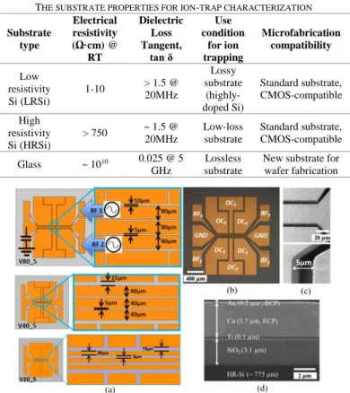
Fig.1. The ion-trap test vehicles with RF and DC biasing set-up and metal layers structural composition. (a) The three variations of design vehicles (V20_5, V40_5, and V80_5) with their respective RF and GND lines dimensions. Version V80_5 has the line width of 80 μm while the smallest version V20_5 has line width of 20 μm.(b) The biasing set-up for the ion trap that consists of RF excitation, central GND and DC biases & (c) The SEM picture of die with the metallization spacing measurement. (d) The cross-section of die photo which shows the actual built of metallization thickness (Ti-Cu-Au) layers.
as compared to Si substrate, back-grinding, and polishing process required can be avoided in glass substrate due to its scalable thickness (down to 100 µm) [2]. Possibilities to fabricate blind-vias and through glass vias (TGV) further extends the benefit of glass substrate for ion-trap implementation [3], as 3D integration with TGV and multi-layer metallization option are essential features in multi-qubits quantum computing system, where up to thousands of RF and DC electrodes are required. Besides, by adjusting their coefficient of thermal expansion (CTE) to be close or even equal to Si substrate [4], the ion trap on glass can also be integrated into silicon substrate to combine the high-performance ion trap on-glass with other Si-circuit building blocks such as digital-to-analog converter, voltage regulator, low-pass filter, RF source, etc. to obtain full system integration. Such hetero-structure ion-trap design had been reported in [5].
Besides glass substrates, silicon substrates have also been explored in ion trap implementation for their CMOS-compatible fabrication process and high density integration technologies such as the through silicon via (TSV) interconnection and multilayer metallization, which are particularly useful for multi-qubits quantum computing system [6]-[12]. However, the high RF loss of Si hinders its feasibility in full-silicon integrated ion trap system scheme [13]-[18]. Some possible solutions have been proposed, such as the introduction of grounding layer, increasing the insulation layer (SiO2) thickness (up to 10μm), lowering the work temperature (<10K), etc. In our design, by utilizing high resistivity silicon substrate (> 750Ωcm), both leakage current and loss tangent of silicon substrate can be reduced. Therefore, a favorable RF performance is expected.
In order to characterize their performance difference, we developed both ion-traps on glass and Si substrate with identical design geometry. Corresponding RF analysis and characterization as well as performance benchmarking are presented. The on-chip performances such as the insertion loss, capacitance stability, Q factor, power efficiency, power spectral density, power dissipation are tabulated for comparison. We have also integrated the chips into the standard CPGA packaging to verify their on-package performances. The final verifications are ion trapping testing by laser optical set-up in ultra-vacuum environment. In this case, the designed ion trap on glass successfully confines ion with lifetime tens of minutes under 110Vpp and 39 MHz of RF excitation.
This study begins with the overview of the fundamentals of
quantum computing and surface electrode ion-trap
implementation on glass and Si substrate in Section I. Next, RF analysis is presented in Section II and ion-trap resonance characterization is elaborated in Section III. After that, the microfabrication process of the ion-traps is presented in Section IV, where the integration of fabricated traps into the CPGA packaging is discussed in Section V. Section VI shows the optical measurement set-up that has successfully captured single 88Sr+ ion. Lastly, the key findings are concluded in Section VII.
II. RFCHARACTERIZATION TABLEI
THE SUBSTRATE PROPERTIES FOR ION-TRAP CHARACTERIZATION
Substrate type Electrical resistivity (Ω·cm)@ RT Dielectric Loss Tangent, tan δ Use condition for ion trapping Microfabrication compatibility Low resistivity Si (LRSi) 1-10 > 1.5 @ 20MHz Lossy substrate (highly-doped Si) Standard substrate, CMOS-compatible High resistivity Si (HRSi) > 750 ~ 1.5 @ 20MHz Low-loss substrate Standard substrate, CMOS-compatible Glass ~ 1010 0.025 @ 5 GHz Lossless substrate
New substrate for wafer fabrication
TABLEII
THE DIMENSION OF RFELECTRODES OF THE DESIGN VEHICLES
Design vehicles Dimension of RF electrodes (G-S-G) lines Chip area L×W (mm2) RF line width (μm) Spacing (μm) Length (μm) V20_5 20 5 730 1.8×1.8 (3.24) V40_5 40 5 1460 3.9×3.9 (14.90) V80_5 80 5 2920 7.9×7.9 (62.4)
Fig. 1 shows planar surface-electrode ion-trap designs with three design variations (V20_5, V40_5, and V80_5), which are used to characterize the insertion losses, capacitances and also the Q factors of the ion-traps due to devices scaling and substrate variations. Their associated dimensions are given by Table II. Each of ion-trap design on Si substrate has similar metallization layers composition, which consists of three sandwiched metallization layers (Ti (0.1µm), Cu (3.7µm), and Au (0.2µm)) on top of silicon dioxide. The main differences among the test vehicles are the width and length of the RF and ground lines. Upon the application of RF signal, electric field
Fig.2. Comparison of E-field characteristic of RF-excited ion-traps on HRSi, LRSi and glass at 60MHz. (a) and (b) E-field on HRSi and LRSi respectively, with high stray E-field on exposed oxide layer. (c) The E-field characteristic of ion trap-on-glass with low stray E-field but high E-field density around the trapping zone.
Low stray E-field
High stray E-field
High stray E-field
High E-field Density
(a) HRSi
(b) LRSi
(c) Glass
(E-field) will be excited from RF lines and terminated into the ground line for the formation of pseudopotential.
Fig.2 shows the E-field characteristic distributions of the ion-traps test vehicles on high resistivity silicon (HRSi), low resistivity silicon (LRSi) and glass respectively. As shown in Fig.2(a) and (b), both ion-traps designs on HRSi and LRSi produce high stray E-field (in the order of 103 – 104 V/m) as observed around the exposed dielectric area (non-metallized area). These amounts of stray E-field increase power dissipation and parasitic capacitance, which lead to higher resonance loss and lower Q factor [19]. Subsequently, lower Q value increases the power bandwidth and reduces the power spectral density (PSD) [20]. The reduction in power spectral density indicates that more power is needed to be delivered to the ion trap to form the pseudopotential. Hence, the end product of this stray of E-field is in the form of heat dissipation which affects the overall operation of the quantum computing system.
On the other hand, the E-field distribution of itrap on-glass shows higher density around the central lines (in the area around the two RF lines that sandwich the ground line). The stray E-field around the exposed substrate is also showing lower density than the observation on HRSi and LRSi. Based on this E-field quality, ion-trap on-glass is expected to have higher quality factor, lower power dissipation, and higher power spectral density.
Fig.3 demonstrates the superiority of ion-traps on-glass in terms of RF performances as compared to their Si counterparts, which are highly dependent on Si substrate conductivity. As the substrate resistivity increases, the insertion loss increases at low frequency region but improves at high frequency region. This can be attributed to the dominance of Ohmic loss at low frequency; while substrate
loss is dominant at high frequency. Between these frequency regions, a transition frequency exists, which is defined as the frequency point where the effect of Ohmic loss is equal to the substrate loss.
The insertion loss of the ion-trap on glass is around 0.2dB, which is far more superior to the ion-trap performances on any variation of substrate conductivity of Si substrate. This is also confirmed by the measurement results as given by Fig.4. Fig. 3(b) shows the shift in transition frequency due to device scaling. Overall, the high resistivity Si substrate (HRSi) gives better insertion loss performance than low resistivity Si substrate (LRSi) at frequency higher than transition frequency. Understanding this substrate conductivity related behavior is very critical in choosing which Si substrate is more appropriate for certain ion-trap design dimension.
In order to choose which silicon substrate resistivity will give better performance, we need to map the transition frequencies of the substrates with respect to the resonance frequency as given by Fig.3 (a). When the resonance frequency is set to be equal to 75MHz (higher than transition frequency (43MHz)); the high resistivity silicon substrates have better insertion loss than low resistivity substrates. However, if the resonance frequency is set to be equal to 25MHz (lower than transition frequency (43MHz)); the lower resistivity substrates have better insertion loss than high resistivity substrate. Therefore, the choice of silicon substrate resistivity is fundamentally determined by the applied RF excitation frequency and relative position of transition frequency with respect to the resonance frequency.
Fig.5. Comparison between extracted capacitance on simulation and measurement of ion-trap version V40_5 on HRSi, LRSi and glass respectively.
Stable glass capacitance Un-stable Si-capacitance
Fig.4. Variation in insertion loss performances (measurement) on low resistivity silicon (LRSi) substrate, high resistivity silicon (HRSi) substrate and on glass. (a) Full comparison. (b) Zoom around the glass insertion loss responses to show on-glass performances superiority.
0.00 100.00 200.00 Freq [MHz] -0.12 -0.10 -0.08 -0.06 -0.04 -0.02 In se rt io n L o ss (d B ) XY Plot 7 V20_Glass V40_Glass V80_Glass (a) (b)
Fig.6. The comparison between simulation and probing measurement of ion-trap Q factor showing the Ohmic loss effect at frequency range below 50 MHz and effect of parasitic inductor to the measured Q factor of ion-trap on-glass. Ohmic-contact loss Parasitic inductor effect (a) (b)
Fig.3. The ion-trap on glass superior insertion loss performance compared to Si counterparts and the transition frequency defining the frequency range of Ohmic loss region or substrate loss region of silicon substrate. (a) Change in insertion losses due to variation in substrate conductivities with distinction in glass performance. (b) Shift-up in transition frequency due to device scaling of ion-traps on Si substrate.
0.00 25.00 50.00 75.00 100.00 Freq [MHz] -7.50 -6.25 -5.00 -3.75 -2.50 -1.25 0.00 In se rt io n L o ss (d B ) XY Plot 2 Curve Info R800 Imported R1 Imported G10 Imported G20 Imported R10 Imported R1000ohm Imported R100 Imported Glass Imported LR_Si: Rsub <10 Ω HR_Si: Rsub > 100 Ω Substrate loss region Ohmic loss region Glass V80_5 X:47MHz Y:2.5dB X:129MHz Y:1.6dB X:436MHz Y:1.0dB V40_5 V20_5
Smaller device Transition frequency shifted-up V20_LRSi V20_HRSi V40_LRSi V40_HRSi V80_LRSi V80_HRSi
III. RESONANCE CHARACTERISTIC
A. Equivalent Capacitance & Q Factor
Ion trap is a capacitive device and its capacitance is built by
E-field excitation. The E-field fluxes are coming out from the
pair of RF lines and terminate themselves into the central ground lines. Assuming the phases of RF signal sources into the RF lines are perfectly balanced, there will be E-field cancelation along the axial confinement (axis of central ground lines). Depending on the width and spacing between RF and central ground lines, the pseudopotential will be zero at certain height above axial confinement and maximum in the area between the RF line and ground line. The potential difference between the minimum (zero level) and maximum defines the height of trapping potential (meV), which correlates to the kinetic energy needed by the trapped ions to escape from this trapping potential.
The profile of the pseudo-potential is reflected into the equivalent capacitance of the ion-trap. Uniform pseudo-potential along the axis of confinement is indicated by stable
capacitance value across the bandwidth of operation. When the capacitance is non-linear (un-stable) across the operating frequency, lower Q factor is produced. This can be translated to lower power spectral density and worse power efficiency.
Fig.7. The resonance condition of ion-traps on three evaluated substrates (HRSi, LRSi, and glass) for the three variant of test vehicles (V20_5, V40_5, V80_5). (a) The resonance condition of ion traps on HRSi which show the comparison between simulation results (solid lines) and measurement results (dotted lines). (b) & (c) The resonance condition the counterpart on LRSi and glass respectively. In this case, the resonance peaks of HRSi and LRSi are around - (18 – 20 dBm) for V20_5, around -25 dBm for V40_5 and - (30 – 32 dBm) for V80_5. On another hand, the resonance peaks of ion-trap on-glass are about 1 – 4.2 dBm.
Fig.8. The ion-trap power spectral density measurement. (a) The ion-trap on-glass power spectral density due to 60 MHz RF input source excitation. (b) and (c) The respective power spectral density of ion-trap on HRSi and LRSi respectively.
(a) (b) (c)
So, non-linear Si capacitor behavior as shown by Fig.5 is undesirable effect in ion-trap design.
Capacitive devices exhibit Q factor responses profile in the form of hyperbolic curves. The existence of parasitic resistance and inductance will influence the shape of this hyperbolic curve. Series parasitic resistance will result in reduction of power resonance peak and broader bandwidth of power density, which can be translated to lower attainable Q factor. Hence, ion trap with longer RF line will have lower Q factor due to higher equivalent series resistance (ESR). During the measurement, the effect of series resistance can also be added by Ohmic contact-losses that are introduced by the physical contact between probing tips and the metallization surfaces of the ion-trap. The effect of the Ohmic contact-losses can be seen in Fig.6 at frequency below 50-MHz. In this case, the Ohmic contact-losses have significant effect to the Q factor of ion-trap on LRSi. This can be attributed to the low equivalent series resistance (around 5 - 15 Ohm) in the ion-trap on LRSi. So, the Ohmic-contact resistance around 10 Ohm will reduce its Q factor by factor of ~2. On the other hand, this Ohmic-contact resistance only changes the equivalent resistance of HRSi (600 – 800-Ohm) by 8% – 10%, which results in proportional reduction on its Q factor.
The parasitic inductance may significantly alter the hyperbolic response shape of capacitor Q factor at certain frequency range depending on the bandwidth of the parasitic inductance. The Q factor of inductor is zero at DC and is gradually increasing with frequency. The effect of parasitic inductor can be seen in Fig.6 to the Q factor of itrap on-glass. In this case, ion-trap on-glass has measured peak Q factor equal to 974 at 42-MHz. Instead, it gradually decreases following the hyperbolic response curve as simulated; it drops sharply to value close to zero at 51MHz. From 51-MHz to 120MHz, the effect of parasitic inductance dominates the overall Q factor. From 120-MHz onward, the Q factor response of ion-trap on-glass shows the continuation of hyperbolic-curve response as in simulation.
B. Resonance Condition
Fig. 7(a)-(c) show the comparison between simulation and measurement results of output power responses of ion-trap test vehicles (V20_5, V40_5 and V80_5) on HRSi, LRSi and glass substrates respectively. The output resonance peaks of HRSi and LRSi (with the inclusion of Ohmic-contact loss in simulation) show close agreement between simulation and measurement results. These resonance peaks reflect the
ion-TABLEIII
PERFORMANCE COMPARISON SUMMARY OF ION-TRAP CHARACTERIZATION ON HRSI,LRSI, AND GLASS. Design
Substrate
LRSi HRSi Glass
V20_5 V40_5 V80_5 V20_5 V40_5 V80_5 V20_5 V40_5 V80_5 Insertion loss (dB) 0.2 0.5 3.0 0.5 0.9 4.0 <0.1 <0.1 <0.1 Return loss (dB) 25 17 10 27 18 10 48 48 40 capacitance (pF) @60MHz 1200 2000 8000 1200 2000 3200 100 150 180 Q factor @60MHz 320 380 160 10 15 20 >900 >900 >900 Output power resonance peak (dBm) -30 -25 -21 -30 -24 -20 5 1.8 1.7
Power Spectral Density
PMAX (W) 39 50 50 34 45 48 25 29.5 40 BW3dB (MHz) 10.0 20 48 10.0 20.8 36 1.8 2.0 2.4 P3dB (W) 27.6 35.35 35.35 24.04 31.8 33.94 17.68 20.85 28.28 PSD (W/MHz) 2.76 1.77 0.73 2.4 1.53 0.94 9.82 10.425 11.78
traps power efficiency at resonance frequency of 60MHz. In this case, ion-traps on-glass is 25 – 35 dBm more efficient than ion-traps on Si counterparts. As a consequence, ion-trap on Si substrate will have higher power dissipation, as small fraction of output power is used to form pseudopotential while the remaining power dissipates through the substrate forming stray E-field as illustrated in Fig. 2.
To give more insight about power efficiency, the power spectral densities of ion-traps are calculated based on s-parameter measurement. Power spectral density shows the delivered power into the ion-trap across the bandwidth of resonance. In this case, the 3dB-bandwidth will be used as a reference for the calculation of power spectral density (W/MHz). The power density calculations are summarized in Table 3. As given by Table 3, power spectral density of ion-trap on glass is far superior (9.8 – 11.8 W/MHz) than Si counterpart (only 0.8 – 2.8 W/MHz). As seen in Fig.7(c), ion-traps on-glass exhibit needle-like power density responses that show their efficiency in delivering power from source to the ion-trap metallization for current-to-E-field conversion. This can be correlated to strong E-field concentration around the trapping zone of ion-trap on-glass as illustrated by Fig.2(c).
Power spectral density also suggests the power dissipation outside the passband of frequency response. As seen in Fig. 8(a), the power is near to zero at frequency below 50MHz and above 80MHz of ion-trap on-glass frequency responses. This postulates that the power dissipation outside the PSD passband is near to zero Watt. On the other hand, ion-trap on HRSi and LRSi show power level of 24 – 35W outside their 3dB power bandwidth, which indicate ion-traps on Si substrate have significantly higher power dissipation than glass substrate. These can also be correlated to E-field distribution of ion-trap
on HRSi and LRSi which show large stray E-field density around the exposed (non-metallized) silicon area.
IV. MICROFABRICATION
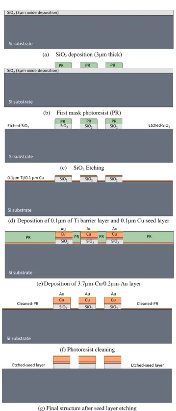
The microfabrication of ion-traps on LRSi and HRSi are done in 300mm Si wafer platform as illustrated by Fig.9. First, the 3µm SiO2 layer is formed by low-stress Plasma-Enhanced Chemical Vapor Deposition (PECVD). After patterning and dry etching of the insulation layer, 0.1µm Ti adhesion layer and 0.1µm Cu seed layer are subsequently deposited on top of the insulation layer. Next, 3.7µm Cu and 0.2µm Au layers are deposited by electrochemical plating (ECP) process. In the end, metal seed layer will be etched back to avoid shorts especially between RF and ground electrodes.
On the other hand, the microfabrication of the ion-trap on glass is more straightforward. Due to the use of glass substrate, the original insulation layer between silicon and metal electrodes can be eliminated. Adhesion layer and seed layer are directly deposited on the glass substrate. Same process as described above will be utilized for electrode patterning. However, to simplify seed layer etching process, a Cu layer with reduced thickness (2.5 µm) is used.
The first challenge in microfabrication of the ion-traps is the leakage current that flow from one conductor to another via the substrate. Due to large applied peak-to-peak voltage (200Vpp – 250Vpp) into the RF electrodes, the leakage current will result in huge power dissipation. To minimize the leakage current, thick SiO2 insulator layer is deposited on top of Si substrate. The use of high resistivity silicon substrate further minimizes the leakage current. Another challenge is on the etching of metal seed layer especially between RF and ground electrodes.
(f) Photoresist cleaning
(g) Final structure after seed layer etching
Fig.9. Microfabrication process schematic for ion-trap on silicon substrate (not to scale).
Si substrate
SiO2 SiO2 SiO2
Cleaned-PR Cu Cu Cu Cleaned-PR
Au Au Au
Etched-seed layer Etched-seed layer
(b) First mask photoresist (PR)
(c) SiO2 Etching
(d) Deposition of 0.1μm of Ti barrier layer and 0.1μm Cu seed layer
(e) Deposition of 3.7µm-Cu/0.2µm-Au layer Si substrate
2
Si substrate
Etched-SiO2 PRSiO2 SiOPR2 SiOPR2 Etched-SiO2
Si substrate
SiO2 SiO2 SiO2
0.1μm Ti/0.1 μm Cu
Si substrate
SiO2 SiO2 SiO2
PR Cu PR Cu PR Cu PR
Au Au Au
Fig.12. The structure of microfabrication of the ion-traps on Si substrate with detail zoom into the gap between electrodes.
Fig.13. The structure of microfabrication of the ion-traps on glass substrate with detail zoom into the metallization thickness area.
Fig.11. Cu oxidation issue. (a) Image from optical microscope. (b) SEM image.
Fig. 10 shows the Cu seed residue remained in between the electrodes during the seed layer etching process. Narrow gap and high sidewall make it difficult for complete etching. Cu residue can be detected by applying low peak-to-peak RF signal (1 – 5Vpp) into the electrodes of the ion-traps and
observing their s-parameters (insertion loss, return loss and impedance characteristic) with respect to reference known-good part. In this case, the residue will affect insertion loss of the ion-trap and the amount of drop to insertion loss will depend on the amount of residue. Large Cu residue (as in Fig. 10(a)) can be visually inspected and cause large drop in insertion loss, that easily identifiable during the RF testing. However, little Cu residue may not significantly affect the insertion loss performance and can be undetectable during the RF testing. Despite insignificant effect in RF testing, little Cu residue possesses hidden threats in causing electro-static discharge (ESD) during ion-trap testing in ultra-vacuum environment when large peak-to-peak voltage (200Vpp – 250Vpp) is applied into the electrodes, as shown by Fig. 10(b). Therefore, it is essential to obtain smooth conductor edges for lower susceptibility to ESD. As ESD often occurs from the accumulation of concentrated charges in pointy (non-smooth) regions, smooth edges as shown in Fig. 10(c) is necessary to prevent ESD.
Fig. 10. Microfabrication of the ion-traps (top view): (a) Die with Cu residue. (b) ESD damage due to Cu residue upon application of RF voltage. (c) Smooth edge of good die.
Fig. 14. Integration of ion-trap into CPGA packaging using bonding wire as interconnects. (a) Top view with RF and DC bias excitation. (b) Elevation view. (c) The bird-eye view. (d) Sample picture of final integration of ion-trap chip (V40_5) into CPGA packaging with bypass capacitor.
Fig.15. Comparison between simulation and measurement of output power of ion-trap chips on CPGA packaging with bonding wires interconnects. (a) Output power of V40_5. (b) Output power of V80_5.
(a)
(b) Copper can actively interact with oxygen to form cuprous
oxide (Cu2O) or cupric oxide (CuO), which affects the overall conductivity of copper. High surface roughness in copper may also increase the oxidation rate due to high surface area interaction. This oxidation issue on ion-trap metallization (as shown in Fig.11) reduces the strength of E-field due to the increase in resistivity of the copper surface. Hence, a thin layer of Au is deposited on top of copper layer to overcome this oxidation problem. Fig.12 and Fig.13 show the final microfabrication of surface electrode ion-traps on Si and on glass substrate respectively.
V. ON-PACKAGING PERFORMANCE
Fig.14 shows the modeling of ion-trap chip on CPGA packaging with bonding wire interconnections. The RF lines are excited by 200V peak-to-peak RF voltage. Such a high voltage swing can affect the DC biasing condition through inductive coupling via the bonding wires. Change in DC biasing condition may affect the axial confinement and ion position may shift accordingly along the ground line axis. This will increase the complexity of ion addressing since laser spatial accuracy of ten-to-hundreds of nm is needed. To minimize the inductive coupling from RF bonding wires to DC wires, the RF excitation and DC biasing set-up are orthogonally connected to side pins of CPGA packaging to minimize cross-talk.
Fig.15 shows the measured output power resonance condition (dBm) of ion-trap chips on CPGA packaging. To avoid excessive power injected into the oscilloscope, capacitive power divider of C1:C2 = 1:20 is used. Hence, the peak output powers are about 20 – 20dBm lower than calculated values as given by Fig.7. Some discrepancies on the peaks of output power resonances are found, which can be attributed to cable losses and capacitor losses. The cables
VI. ION-TRAP TESTING
Fig. 16(a) shows the laser optical set-up which successfully captures an 88Sr+ion for single qubit quantum operation. 88Sr+ is used as the targeted ion qubit in this work due to its simple level structure and the availability of laser diodes for all relevant atomic transitions [21], [22]. For quantum computing operation in 88Sr+ ion, 422nm, 674nm, 1033nm and 1092 nm lasers are used to induce the laser-atom interactions for inter-state transitions, as shown in Fig.16 (b) [23]. Fundamentally,
clock transition laser is also used for |0⟩ to |1⟩ state transition (S1/2 to D5/2 orbital transition). D5/2 is selected as the |1⟩ state due to its relatively long (~0.35s) lifetime. Meanwhile, for |1⟩ to |0⟩ state transition, 1033 nm clear-out laser is used in driving the D5/2 to P3/2 orbital transition, which will be spontaneously decay to S1/2 orbital, or (|0⟩ state) due to short lifetime in P3/2 orbital, as shown in Fig.16(b). A coherent superposition of the S and D states, D3/2 is known as the Dark State which will hinder state transitions in 88Sr+ ion. Therefore, the D3/2 state needs to be continuously re-pumped to maintain cooling using 1092nm re-pumping laser [25], [26]. For state detection, the electron shelving technique is used to distinguish the S and D states, which corresponds to |0⟩ and |1⟩ states. The S state is coupled to the P state with a strong transition, which is continuously driven with the Doppler cooling laser at 422nm. If the ion is in the S state, photons are scattered and the ion fluorescence can be detected. If the ion is in the D state, no fluorescence is detected [25]. Thus, besides Doppler cooling, 422nm laser can also be used for S/D states detection.
VII. CONCLUSION
The ion-trap on-glass was tested to exhibit superior performance than ion-trap on-silicon in all design consideration parameters (insertion loss, Q factor, capacitance stability, power efficiency, power spectral density, and E-field density). In particular, glass ion-trap was tested to have significantly higher Q factor than its silicon counterparts. Such high Q factor leads to higher power efficiency and power spectral density (PSD). Glass ion-trap was also proven to have superior insertion loss performance. Due to its lossless properties, glass substrate was demonstrated to have low of stray E-field on the exposed surface (non-metallized area) but very high E-field density around trapping zone. Glass ion-trap was showed to have a more stable and linear equivalent capacitance, which gave more efficient current-to-E-field transformation. Based on the obtained results, the microfabrication structures were demonstrated to perform the ion-trapping functionality as simulated. With the success of capturing the 88Sr+ ion, the laser system optical set-up was verified to perform the basic steps for quantum computing operation. In summary, the reported design and development procedure had been demonstrated to show the single qubit ion-traps functionality for quantum computing system.
REFERENCES
[1] M. Kroner, M. Debatin, J. Mikosch, S. Trippel, E. Just, M. Reetz-Lamour, R. Wester, M. Weidemuller, P. Woias, "Simulation, Design and Test of a Novel Planar RF Micro Ion Trap," TRANSDUCERS
2007 - 2007 International Solid-State Sensors, Actuators and Microsystems Conference, Lyon, 2007, pp. 1665-1668 [10].
(a)
(b)
Fig.16: (a) Laser system optical set-up for Qubit operation (674nm), Doppler cooling and detection (422nm), re-pumping (1033 and 1092nm) and ionization (405nm). (b) Ion-laser interaction in 88Sr+ion for electron ground-state (5s2S
1/2) and excited state (4d2 D5/2) transition (quantum logic |0⟩ to |1⟩ transition) [21].
[2] A. Shorey, J. Keech, G. Piech, B. Wang and L. Tsai, "Glass substrates for carrier and interposer applications and associated metrology solutions," ASMC 2013 SEMI Advanced Semiconductor
Manufacturing Conference, Saratoga Springs, NY, 2013, pp.
142-147.
[3] S. Takahashi, K. Horiuchi, S. Mori, K. Tatsukoshi, M. Ono, M. Mikayama, N. Imajo, T. Moble, "Development of through glass via technology for 3D packaging," 2013 Eurpoean Microelectronics
Packaging Conference (EMPC), Grenoble, 2013, pp. 1-4.
[4] M. Grabowski and W. Jablonski, "The technology of hard glass layers on silicon substrates and their application in microwave semiconductor devices," ASDAM '98. Conference Proceedings.
Second International Conference on Advanced Semiconductor Devices and Microsystems (Cat. No.98EX172), Smolenice Castle,
Slovakia, 1998, pp. 103-106.
[5] J. Britton, D. Leibfried, J. A. Beall, R. B. Blakestad, J. H. Wesenberg, and D. J. Wineland, “Scalable arrays of rf Paul traps in degenerate Si,” Appl. Phys. Lett., vol. 95, 173102, Oct. 2009. [6] D. Leibfried, R. Blatt, C. Monroe, and D. Wineland, “Quantum
dynamics of single trapped ions,” Rev. Mod. Phys., vol. 75, pp. 281– 324, Jan. 2003.
[7] P. See, G. Wilpers, P. Gill and A. G. Sinclair, "Fabrication of a Monolithic Array of Three Dimensional Si-based Ion Traps," in
Journal of Microelectromechanical Systems, vol. 22, no. 5, pp.
1180-1189, Oct. 2013.
[8] S. Hong, Y. Kwon, C. Jung, M. Lee, T. Kim and D. D. Cho, "A New Microfabrication Method for Ion-Trap Chips That Reduces Exposure of Dielectric Surfaces to Trapped Ions," in Journal of
Microelectromechanical Systems, vol. 27, no. 1, pp. 28-30, Feb.
2018.
[9] J. Wang, S. Paesani, Y. Ding, R. Santagati, P. Skrzypczyk, A. Salavrakos, J. Tura, R. Augusiak, L. Mančinska, D. Bacco, D. Bonneau, J. Silverstone, Q. Gong, A. Acín, K. Rottwitt, L. Oxenløwe, J. O’Brien, A. Laing, and M. Thompson, "Large-scale Integration of Multidimensional Quantum Photonics Circuits on Silicon," 2018 Conference on Lasers and Electro-Optics (CLEO), San Jose, CA, 2018, pp. 1-2.
[10] M. Y. Simmons, "Quantum computing in silicon," 2015 IEEE
International Electron Devices Meeting (IEDM), Washington, DC,
2015, pp. 1.2.1-1.2.4.
[11] J. M. Amini, H.Uys, J. H. Wesenberg, S. Seidelin, J. Britton, J. J. Bollinger, D. Leibfried, C. Ospelkaus, A. P. VanDevender and D. J. Wineland," Toward scalable ion traps for quantum information processing," New Journal of Physics, Volume 12, March 2010. [12] K. K. Mehta, A. M. Eltony, C. D. Bruzewicz, I. L. Chuang, R.J. Ram,
J. M. Sage and J. Chiaverini," Ion traps fabricated in a CMOS foundry," Applied Physics Letters. 105. 10.1063/1.4892061. [13] D. Stick, W. K. Hensinger, S. Olmschenk, M. J. Madsen, K.
Schwab and C. Monroe ," Ion trap in a semiconductor chip," Nature Physics 2, 36–39 (2005)
[14] S. X. Wang, Y. Ge1, J. Labaziewicz, E. Dauler, K. Berggren, and I. L. Chuang," Superconducting microfabricated ion traps," Appl. Phys. Lett. 97, 244102 (2010)
[15] S. C. Doret, J. M. Amini, K. Wright, C. Volin, T. Killian, A. Ozakin, D. Denison, H. Hayden, C.-S. Pai, R. E. Slusher," Controlling trapping potentials and stray electric fields in a microfabricated ion trap through design and compensation," New Journal of Physics, Volume 14, July 2012
[16] D. T. C. Allcock, J. A. Sherman, D. N. Stacey, A. H. Burrell, M. J. Curtis, G. Imreh, N. M. Linke, D. J. Szwer, S. C. Webster, A. M. Steane and D. M. Lucas," Implementation of a symmetric surface-electrode ion trap with field compensation using a modulated Raman effect," New Journal of Physics, Volume 12, May 2010.
[17] S. Hong, M. Lee, H. Cheon, J. Ahn, M. Kim, T. Kim, D. D. Cho, "New scalable microfabrication method for surface ion traps and experimental results with trapped ions," 2015 28th IEEE
International Conference on Micro Electro Mechanical Systems (MEMS), Estoril, 2015, pp. 292-295
[18] J. Tao, N. P. Chew, L. Guidoni, Y. D. Lim, P. Zhao and C. S. Tan, "Fabrication and Characterization of Surface Electrode Ion Trap for Quantum Computing," 2018 IEEE 20th Electronics Packaging
Technology Conference (EPTC), Singapore, Singapore, 2018, pp.
363-366.
[19] J. Wesenberg," Electrostatics of surface-electrode ion traps," Phys. Rev. A 78,063410 (2008).
[20] D. Gandolfi, M. Niedermayr, M. Kumph, M. Brownnutt, and R. Blatt, "Compact radio-frequency resonator for cryogenic ion traps," The Review of scientific instruments. 83. 084705. 10.1063/1.4737889.
[21] S. X. Wang, “Quantum gates, sensors, and systems with trapped ions,” Massachusetts Institute of Technology, 2012.
[22] “Large two dimensional Coulomb crystals in a radio frequency surface ion trap,” Appl. Phys. Lett., vol. 100, no. 17, 2012.
[23] C. D. Bruzewicz, J. Chiaverini, R. McConnell, and J. M. Sage, “Trapped-ion quantum computing: Progress and challenges,” Appl.
Phys. Rev., vol. 6, no. 2, 2019.
[24] J. P. Likforman, V. Tugayé, S. Guibal, and L. Guidoni, “Precision measurement of the branching fractions of the 5p P1/2 2 state in Sr + 88 with a single ion in a microfabricated surface trap,” Phys. Rev. A, vol. 93, no. 5, pp. 1–21, 2016.
[25] G. Higgins et al., “Single Strontium Rydberg Ion Confined in a Paul Trap,” Phgysical Rev. X, vol. 021038, pp. 1–11, 2017.
[26] M. G. House, “Analytic model for electrostatic fields in surface-electrode ion traps,” Phys. Rev. A - At. Mol. Opt. Phys., vol. 78, no. 3, pp. 1–8, 2008.
Anak Agung Alit Apriyana received
the B.Eng and M.Phil degree from the Nanyang Technological University (NTU), Singapore, in 2003 and 2004 respectively, majoring in RF circuit design, and the Ph.D. degree from NTU in 2015.,He worked at TDK-EPCOS Pte Ltd., Singapore, for five
years as a Senior Product
Development Engineer. He was in charge of the design and development of radio frequency integrated circuit surface acoustic wave (RF IC SAW) filters. He then joined NTU since January 2010, as a Researcher at the Virtus IC Design Centre, while pursuing his P.D. degree under IC design scholarship by the Economic Development Board of Singapore.
Hongyu Li received the Ph.D. degree
in semiconductor physics and devices from the Changchun Institute of Physics, Chinese Academy of Science, China, in 1999. She is working on the process integration and reliability improvement for 3-D through-silicon- via (TSV) technology, wafer level Cu/Cu hybrid bonding and surface ion trap, as a senior scientist in the Institute of Microelectronics, Agency for Science, Technology and Research, Singapore. She has published more than 50 research papers and 5 Patents.
Peng Zhao (S’2020) received his B.E.
degree in mechanical and material engineering from Tianjin University, Tianjin, China, in 2018. He is currently working toward the Ph.D. degree at Nanyang Technological University, Singapore. His Ph.D. focus area is design, modelling and characterization of surface electrode ion trap integrated with TSV and photonic devices.
Deggendorf, Germany, in 2008. She worked as product quality engineer in Zollner Electronic, China, from 2008 to 2011. Then she began her doctoral work in Tyndall National Institute, University College Cork, Ireland and received her Ph.D. degree in microelectronics in 2016. She is currently a research fellow at Nanyang Technological University. Her current research interests include surface ion trap technology for quantum computing, TSV technology and 3D system integration.
Yu Dian Lim received the B. Eng. in
Materials and M. Sc. of Materials Engineering from University of Malaya (UM), Malaysia, in 2011 and 2014, respectively. After that, he received the
PhD in EEE from Nanyang
Technological University (NTU), Singapore in 2018. He is currently holding a postdoctoral research fellow position in School of Electrical and Electronic Engineering, NTU. He has involved in multidisciplinary researches,
including nanomaterials, MEMS fabrication,
communication device design etc. His current research interests include silicon photonics integrated circuit design and quantum computing.
Ye Lin (S’16-M’19) received his B.S.
degree (2013) and Ph.D. (2019) from the School of Electrical and Electronic Engineering, Nanyang Technological University (NTU), Singapore. His research interests are integrated passive devices and 3-D integrated circuits.
Luca Guidoni received the Ph.D.
degree at Pierre et Marie Curie University Paris, France, in 1998. He currently holds a CNRS researcher position at the MPQ laboratory of the Denis Diderot University in Paris. His research activity is mainly devoted to the experimental aspects of light-matter interaction with a particular interest in quantum optics and laser cooling of atoms and ions.
fall of 2001, he began his doctoral work at the Massachusetts Institute of Technology, Cambridge, USA, and was awarded a Ph.D. degree in electrical engineering in 2006. He is currently a tenured full professor in NTU. His research interests are semiconductor process technology and device physics. Currently he is working on 3D packaging and integration. He is a recipient of the 2019 Exceptional Technical Achievement Award from the IEEE Electronics Packaging Society (EPS). He is a Fellow of the International Microelectronics Assembly and Packaging Society (IMAPS) since 2019.