Anisotropic Dewetting in Ultra-Thin
Single-Crystal Silicon-on-Insulator Films
By
David T. Danielson
B.S. Materials Science and Engineering University of California, Berkeley, 2001
Submitted to the Department of Materials Science and Engineering in Partial Fulfillment of the Requirements for the Degree of
Doctor of Philosophy in Electronic, Photonic and Magnetic Materials at the
Massachusetts Institute of Technology February 2008
OF TEOHNOLOGY
JUN 2 5 2008
LIBRARIES
© 2007 Massachusetts Institute of Technology. All rights reserved.
Signature of Author:
•bepartment of Materials Science and Engineering Nov 20th
,
2007Certified by:
tionel C. Kimerling Thomas Lord Professor of Materials Science and Engineering Thesis Supervisor Accepted by:
Samuel M. Allen POSCO Professor of Physical Metallurgy Chair, Departmental Committee on Graduate Students
Anisotropic Dewetting in Ultra-Thin
Single Crystal Silicon-on-Insulator Films
By
David T. Danielson
Submitted to the Department of Materials Science and Engineering on November 2 0th, 2007 in Partial Fulfillment of the Requirements for the
Degree of Doctor of Philosophy in Electronic, Photonic and Magnetic Materials
ABSTRACT
The single crystal silicon-on-insulator thin film materials system represents both an ideal model system for the study of anisotropic thin film dewetting as well as a technologically important system for the development of the next generation of MOSFET devices. The scientific community has misinterpreted the mechanism behind SOI dewetting, attributing it to a stress-driven instability. In this work, we characterize and measure the kinetics and geometry of thermally-activated dewetting in ultra-thin SOI films as a function of SOI thickness, crystallographic patterned-edge orientation, and temperature. Using experimental data and physical reasoning, we strongly argue against the previously existing scientific consensus that SOI dewetting is a stress-driven instability and present a 5-step isotropic surface-energy-driven dewetting model based upon the capillary film edge instability and the generalized Rayleigh instability, in which we integrate existing theories and in addition develop an expression for the edge retraction distance during the initial uniform edge thickening and retraction phase of dewetting at a patterned mesa edge for the first time, predicting a square root dependence with time and an inverse power dependence on film thickness. In our study, we observe and quantify the kinetics of the initial edge retraction dewetting mechanism experimentally for the first time and confirm the square root time dependence and inverse power law film thickness dependence predicted by our new model. We also quantify the edge dewetting front propagation velocity in SOI and determine that it depends on the negative third power of the film thickness, agreeing with the prediction of Jiran and Thompson and with our model. We also extract an activation energy for the edge dewetting front propagation velocity of 2.9+-0.3eV, in reasonable agreement with reported values for Si surface diffusion on (111) planes. Furthermore, we present for the first time an anisotropic model for void finger propagation that is able to accurately explain the detailed anisotropic dewetting geometries observed in SOI dewetting. A technique for stabilizing ultra-thin SOI films, dielectric layer edge coverage, is also demonstrated that may prove useful to enable the stabilization of ultra-thin SOI films during fully-depleted SOI transistor fabrication. We also report on the effect of Ge coverage on SOI dewetting kinetics.
Thesis Supervisor: Lionel C. Kimerling
Acknowledgements
I would like to first and foremost thank my thesis advisors Professor Lionel C. Kimerling and Jurgen Michel for their profound intellectual, emotional, and financial support throughout the course of my thesis work at MIT.
I would also like to thank the other members of my thesis committee, Professors Carl V. Thompson and W. Craig Carter. Professor Thompson's passion and enthusiasm for the topic of dewetting filled my reserves when they were down and his deep knowledge of the field pointed me in the right direction innumerable times. Professor Carter was incredibly helpful in providing a number of insights into the capillary behavior of solid state materials, especially the effects of surface energy anisotropy.
I would also like to thank the many collaborators who were instrumental to the completion of this work. I would like to especially emphasize the support that Intel Corporation provided me in this work. Intel graciously hosted me to work on SOI dewetting at their prestigious Components Research Division in Oregon during the summer of 2005. Furthermore, without the generous supply of state-of-the-art SOI material by Intel, this thesis work would not have been possible. I am particularly indebted to Mohamad Shaheen, Peter Tolchinsky, Joanne Qiu, and Micheal McKeag from Intel for all of their individual efforts as excellent collaborators. I am also forever indebted to the team of staff and fellow graduate students who helped me maintain (and frequently rebuild) the Kimerling EMAT group's UHV-CVD system, upon which this work depended heavily. MIT MTL staff member Bob Bicchieri went above and beyond the call of duty a thousand-times and fellow EMAT members Anat Eshed, Jifeng Liu, Nok Jongthammanurak, and Douglas Cannon were an absolute pleasure to work with as I learned how to turn a bolt. I would also like to thank the many members of the MIT MTL staff who were incredibly supportive at every turn during the semiconductor processing required in this work, including Bob Bicchieri, Donal Jamieson, Dave Terry, Paul Tierney, Kurt Broderick, and Bernard Alamiriu. I would specifically like to thank Vicky Diadiuk for always being incredibly supportive and finding solutions when I got lost in the processing matrix maze at MTL.
I would like to thank the "Silicon Wafer Engineering and Defect Science" (SiWEDS) NSF Industry/University Cooperative Research Center for providing significant financial and mentorship support for my thesis work. Through SiWEDS, I got the opportunity to give my first public scientific talk and to become part of a broader scientific community for the first time. I am especially thankful to SiWEDS director and NCSU Professor George Rozgonyi, who has provided me with caring mentorship and direction throughout the course of this work. I would also like to thank the United States Department of Defense for providing me full fellowship support during my first three years at MIT through a National Defense Science & Engineering Graduate Fellowship.
I am also deeply thankful to those individuals whose academic tutelage gave me the basic tools and understanding to allow me to be the scientist I am today. I wholeheartedly thank the Department of Materials Science & Engineering at the University of California,
Berkeley for giving me the best undergraduate materials education I could have ever hoped for. I am particularly thankful to Professors Tim Sands, Ron Gronsky, and Eugene Haller for lighting an academic fire in my mind and in my belly. Most importantly, I would like to thank my undergraduate advisor and beloved mentor from U.C. Berkeley, Professor Andreas M. Glaeser, for everything.
A complete education at MIT is also more than experiments, lectures, characterization, analysis, and writing. At MIT, I learned almost as much about leadership and community development as I did about dewetting. Outside of my research experience at MIT, my experience founding and growing the MIT Energy Club and the MIT Energy Conference has been my one true joy. I only wish that I had the space here to acknowledge and thank the hundreds of MIT students, faculty, and alumni with whom I have had the distinct pleasure to work through the MIT Energy Club. I am immensely thankful to Joost Bonsen for teaching me how to make my passion and ideas become reality; to Nol Browne for teaching me everything I know about business; to Mike Berlinski for being there when no one else was; and to Libby Wayman, Kristian Bodek, Nol Browne, Brian Walsh, Alissa Jones, James Schwartz, and Daniel Enderton for being the best colleagues one could every ask for.
On a more personal note, I would like to thank all of those who offered support of a more emotional nature over the years as I worked toward completing this thesis work. My parents, Paul and Margaret Danielson, offered constant and unwavering love and support through the highs and lows of 6.5 years of PhD research. I thank fellow EMAT colleagues and friends Jifeng Liu, Nok Jongthammanurak, Anu Agarwal, and Jurgen Michel for always being there for me when I needed an ear. Without the ability to complain to and hear the complaints of my fellow grad students and best pals Ryan Williams and Dan Sparacin over the years, I don't think I would have made it. And very importantly, I offer huge thanks to Anu Agarwal and MIT Professor Sam Allen for getting me through my toughest moment.
Table of Contents
TITLE PAGE ... 1 ABSTRACT ... ... 3 ACKNOWLEDGEMENTS... 5 TABLE OF CONTENTS... 7 CHAPTER 1: Introduction... 8CHAPTER 2: Literature Review - Dewetting in Thin Solid Films... 22
CHAPTER 3: Literature Review -Dewetting in Silicon-on-Insulator Films... 42
CHAPTER 4: Surface-Energy-Driven Model of SOI Dewetting ... 52
CHAPTER 5: SOI Dewetting Study - Experimental Details... 82
CHAPTER 6: SOI Dewetting Study - Experimental Results and Discussion... 91
CHAPTER 7: Future Work... 131
CHAPTER 8: Summary and Conclusions... 135
APPENDIX A: Anisotropic Surface Energies in SOI Films... 137
APPENDIX B: Effect of Ge Coverage on Dewetting in SOI Films... 142
Chapter 1:
Introduction
As materials dimensions shrink into the nanoscale, surface effects become
increasingly important and will tend to dominate materials behavior in structures with
sufficiently small dimensions. This is due to the geometrical fact that the surface
area-to-volume ratio of a structure scales with the inverse of the structure's characteristic
dimension, re, as illustrated in Figure 1.1. For this simple reason, nanoscale structures
possess an immense amount of surface energy and thus have an extremely high driving
force to evolve morphologically to lower their surface energy. This presents major
challenges for the fabrication of ever-shrinking nanodevices and also, interestingly,
presents the opportunity to use surface-energy-driven instabilities to fabricate useful
nanostructures. Friend or foe: surface-energy-driven morphological evolution will
become ever more important as we continue to dive deeper into the realm of
nanotechnology.
Dewetting in ultra-thin (< 30nm) silicon-on-insulator (SOI) films has emerged as
a very important example of this increased susceptibility of nanometer-scale structures to
surface-energy-driven morphological instabilities. This surface-energy-driven layer
instability has significant implications both for furthering our understanding of the basic
science of surface-energy-driven morphological instabilities, as well as for the
(a)
Area 4ryR 2 _ 11Volume
4 rR3
3R
3
(b)
Area
!2 1
Volume
= 2t
t
Area
1
Volume
r
Figure 1.1: Illustration of the increase in the surface area-to-volume ratio with decreasing characteristic materials dimension in: a.) a spherical particle with radius R, and b.) a thin film with thickness t. As characteristic materials dimensions shrink into the nanoscale, this simple geometrical effect causes surface effects to dominate materials behavior.
Si02
Figure 1.2: Schematic illustration of a silicon-on-insulator (SOI) substrate. The most significant properties of the top Si layer in SOI, from a dewetting perspective, are its single crystallinity and its very low defect density. (Note: The thicknesses of the top Si and SiO2 layers relative to the underlying Si substrate are grossly exaggerated here for the sake of illustration. Typical thickness values for an ultra-thin SOI substrate are: top Si layer - 15nm, SiO2 layer - 145nm, Si substrate -775gm).
tj
SOI is a multilayer thin film structure consisting of a thin layer of crystalline silicon (Si) atop a layer of thermally grown silicon dioxide (SiO2) on top of a standard
silicon wafer, as illustrated in Figure 1.2. Upon high temperature vacuum annealing,
sufficiently thin top Si SOI layers (< 30nm) have been found to dewet from, or uncover,
the underlying SiO2 layer, resulting in the breakdown of the Si film into a discontinuous
array of Si fingers and islands, as show in Figure 1.3.1-11
15nm Si(100)
'0
-- I. ___ Si02 I 800C annealFigure 1.3: Schematic illustration and SEM image of dewetting in an initially continuous, flat 15-nm-thick (100)-oriented top Si SOI layer UHV annealed at 800C for 1360 minutes.
For reference, we provide background here on SOI substrates and how they are
made. Fabricating SOI substrates has been a challenge, as the direct epitaxial growth of
perfect single-crystal layers on amorphous insulators is not possible. There exist two
commercially available types of SOI substrates, termed bonded SOI and SIMOX SOI.
In bonded SOI, a thin single crystal Si layer is transferred to a SiO2 coated Si
wafer using a hydrogen ion implantation/wafer bonding/Si layer exfoliation process. First,
Islanded S1 on S10,1,2
a thin film of Si02 is grown on both a "substrate" and a "donor" silicon wafer using
thermal oxidation. Hydrogen ions are then implanted into the donor wafer through the
SiO2 layer, such that the peak of the implanted hydrogen concentration is a short distance
below the Si wafer's surface. The donor and substrate wafer are then bonded together
such that their SiO2 layers face one another. The bonded sandwich is then annealed at a
low temperature (-650C) at which point the hydrogen present in the donor wafer forms
hydrogen gas filled microvoids at the depth of maximum hydrogen concentration from
the implantation step, which results in crack propagation and exfoliation of the bulk of
the donor silicon wafer, leaving a rough thin crystalline silicon film on the substrate
wafer. The sandwich is then annealed at high temperature (-1200C) to create a strong
bond between the transferred layers and the underlying substrate. The top silicon film is
then annealed and polished to create a finished atomically smooth single-crystal bonded
SOI wafer. The experimental study of dewetting presented in this thesis focuses on bonded SOI substrates.
SIMOX SOI substrates (standing for "Separation by IMplantation of Oxygen")
are fabricated using a quite different process based upon oxygen implantation into a
silicon wafer and the subsequent nucleation and lateral growth of a subsurface layer of
SiO2. Oxygen is first implanted into a silicon wafer, creating an oxygen distribution in the
wafer with a peak at some desired distance below its surface. The wafer is then annealed
at 1200C for a long duration in order to nucleate and laterally grow a buried thin film of
SiO2 beneath a thin crystalline layer of silicon, resulting in a SIMOX SOI substrate. We
compare dewetting in bonded and SIMOX wafers in the experimental work presented in
Here, we briefly motivate and discuss the importance of SOI dewetting from the
three distinct perspectives of basic dewetting science, the integrated circuit industry, and
the field of nanoscale self assembly.
The Scientific Opportunity
From a scientific perspective, ultra-thin SOI represents an important new
materials system available for the study of dewetting science. Ultra-thin SOI is the first
single-crystal thin film dewetting materials system ever made available for study, making
it an ideal model system for the study of the fundamental physical mechanisms behind
thin film dewetting. Model dewetting systems studied until now have been
polycrystalline deposited films with high densities of grain boundaries and other defects,
as well as grains representing multiple crystalline orientations. This high defectivity and
lack of microstructural control has resulted in various types of dewetting behavior being
observed in these systems, as discussed in Chapter 2. Furthermore, the underlying
anisotropic surface energies present in crystalline Si allow anisotropic dewetting to be
observed for the first time in the model SOI dewetting system, presenting us with the
unique opportunity to perform a first-of-a-kind experimental and theoretical study of
anisotropic dewetting.
The Integrated Circuit Industry Challenge
However, from the perspective of the integrated circuit (IC) industry, ultra-thin
SOI dewetting has emerged not as an opportunity, but as a critical process problem that
transistors."'" 12 This is a critical issue for the industry, as it is relying on the imminent
deployment of fully-depleted SOI technology to allow it to continue the exponential
improvements in IC performance and cost that have driven the development of the digital
age. 2
The primary reason that such high quality single-crystal SOI substrates are even
available for dewetting studies is that the IC industry has been forced to develop SOI
substrates in order to enable continued dimensional scaling beyond the "end of the
roadmap" for traditional Si substrate-based metal-oxide-semiconductor field effect
transistors (MOSFET's) to continue Moore's Law-type industry growth, a long time
exponential industry trend in which the number of transistors per chip has doubled every
2 years.13 According to the International Technology Roadmap for Semiconductors, the
use of fully-depleted SOI transistors based upon "ultra-thin" top Si layers (defined as
having top Si layer thickness < 10nm) will be required to deploy the state-of-the-art 45nm
IC technology node in 2010.12
In order to motivate the industrial significance of the development of a
fundamental understanding of SOI dewetting, along with techniques for its suppression,
we explain here why ultra-thin SOI technology is needed by the IC industry and why SOI
dewetting has become a critical process problem for the industry.
During operation of a MOSFET device, a constant voltage is applied between the
source and drain electrodes across the device channel (See Figure 1.4 for a labeled
schematic of a MOSFET device). The voltage applied to the gate electrode controls
device or not (representing either a "1" or "0" in binary code). When an appropriate
non-zero gate voltage is applied, the channel is made conducting and significant current flows
SVgate_
VgO,(on)
0, (off)
drain
Figure 1.4: Schematic of a traditional Si-substrate based MOSFET device.
through the device ("1" or "on" state); when zero gate voltage is applied, the channel
does not conduct and a very low current flows through the device ("0" or "off" state).
The IC industry has almost exclusively used a scaling down of the MOSFET
device gate length (Lg) to enable the exponential increases in operating speeds and device
integration density that have driven Moore's Law performance growth. However, as the
industry looks toward the development of its next technology generation (the 45nm
technology node) having a gate length (Lg) of 18nm, it has run up against a fundamental
device problem that requires a move away from traditional Si substrate based devices.
When the gate length is shrunk down to -20nm and below, the device gate electrode
begins to lose control of the conductivity of the channel, yielding control to the source and drain electrodes and to the channel itself (termed "short channel effects"). The loss of control of the channel to the source and drain electrodes results in a choking off of the device current, while the loss of control to the channel itself causes the current to not
completely turn off when the device is in the "off state", resulting in unacceptable
off-state current and power dissipation. Furthermore, the capacitances between the
source/substrate and drain/substrate begin to limit the operating speed of the device.
Moving to fully-depleted SOI transistor technology increases the electrostatic
integrity of deeply-scaled MOSFET's, reducing or eliminating short channel effects. In
fully-depleted SOI MOSFET's, the gate regains control over the channel: reducing the
choking off of device current by the source/drain, providing nearly ideal off-state currents,
and allowing for high speed operation by eliminating the source/substrate and
drain/substrate capacitances.
In order for SOI-based transistors to be fully-depleted, the top Si thickness must
be • 0.3 times the physical gate length (Lg). As seen in Table 1.1, this means that
fully-depleted SOI transistors at the upcoming 45nm technology node will require the use of
SOI substrates with 6.2nm-thick top Si layers; while the 22nm technology node, scheduled to be deployed less than 10 years from now, will require top Si layers as
vanishingly thin as 2.7nm (only 20 atomic layers of Si thick!).12
Year of Year of 2007 2010 2013 20162016 Implementation Technology 65 45 32 22 Node (nm) Actual Gate 25 18 13 9 Length (nm) Fully-Depleted
SOI Top Si N/A 6.2 4.4 2.7
Layer Thickness (nm)
Table 1.1: Future MOSFET technology nodes with expected year of implementation and required top Si
However, these extremely thin top Si layers required for the coming generations
of fully-depleted SOI MOSFET's at and beyond the 45nm technology node have been
found to be highly morphologically unstable to dewetting when vacuum processed at
high temperature, making successful device processing using traditional semiconductor
processes impossible.
The standard semiconductor processing step during which ultra-thin SOI films
have been found to be the most susceptible to dewetting is the raised source/drain
selective silicon epitaxy step. In order to maintain a tolerably low series resistance in
ultra-thin SOI-based MOSFET's, elevated source/drain structures must be grown to
locally thicken the top Si SOI layer via selective epitaxy of silicon on the source/drain
regions of the device, as illustrated in Figure 1.5. This standard IC processing step
consists first of an initial 950C, 2min in-situ hydrogen pre-bake in a silicon epitaxy
vacuum system (known as the "Shiraki clean") to remove the thin native SiO2 layer that
inevitably forms when Si is exposed to air and to remove residual C, 0, and F
contamination typically introduced during previous processing and cleaning steps. This
pre-bake step is immediately followed by selective epitaxy of silicon on the source/drain
regions by pyrolysis of dichlorosilane (SiH2CI2) on the silicon surface at a temperature of
Elevated Source/Drain
SOI LayerI
Si02 I
Figure 1.5: Schematic diagram of a fully-depleted SOI MOSFET showing the elevated source/drain structures required to reduce device series resistance to tolerable levels.
It is the high temperature pre-bake within the selective silicon epitaxy step, during
which the ultra-thin SOI film is exposed to high temperature without the presence of any
stabilizing capping film, that has been found to result most readily in SOI dewetting.
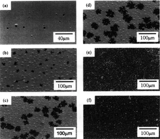
Figure 1.6(a) shows a scanning electron micrograph of an 8nm-thick top Si SOI mesa
after exposure to the standard 950C, 2min hydrogen pre-bake in a selective silicon
epitaxy vacuum system." The top Si film can clearly be seen to have fully dewetted
upon the underlying SiO2 layer under this standard pre-bake condition. Figure 1.6(b)
shows that even pre-bake temperatures as low as 800C result in significant SOI layer
edge retraction, making further device processing difficult, if not impossible.''
It is clear that SOI dewetting during the elevated source/drain pre-bake of
standard MOSFET selective silicon epitaxy process step will only become an even more
severe process limitation as the industry moves to the -6nm, -4nm, and -3nm SOI layer
thicknesses required to deploy fully-depleted SOI transistors at the 45nm, 35nm, and
22nm nodes, respectively, over the next 3 to 10 years. A deeper understanding of the SOI
SOI layers against dewetting during high temperature vacuum processing to enable the successful deployment of fully-depleted SOI MOSFET's.
Initial Si mat border (before nealing) No prebake 800C
900C
(a) (b)Figure 1.6: SEM micrographs of SOI dewetting occurring during the 20 torr H2 Si selective epitaxy
pre-bake step on a patterned 8nm-thick SOI film. a.) Plan view of an 8nm-thick SOI mesa after the standard
950C, 2 min H2 pre-bake. B.) Cross-sectional view of the edge of an 8nm-thick SOI mesa: before pre-bake
(top) and after 2 minute hydrogen pre-bakes at 800C (middle) and 900C (bottom). Note the edge retraction in the case of 800C and the complete dewetting that occurs at 900C."
The Nanoscale Self-Assembly Opportunity
In contrast to representing a major process problem for the development of the
next generation of MOSFET devices, anisotropic dewetting may also represent a
promising new opportunity for "bottom up" self-assembly of highly ordered,
monodisperse nanostructures. The extremely small size and large numbers typically
associated with any assembly of nanoparticles precludes the use of deliberate externally
controlled serial processes to fabricate practical nanostructures. Therefore, scientists have
turned to the concept of self-assembly, in which nanoparticles naturally assemble into
extensive ordered structures without direct ongoing external intervention given
appropriate pre-conditions. A number of rudimentary self-assembling chemical and
compound semiconductor nanocrystal fabricationl4
and self-assembled molecular monolayers on crystalline surfaces'5-17, to the physical processes of solid-state nucleation
and growth of silicon nanocrystals'8
and dewetting of polycrystalline ultra-thin metal films. '9
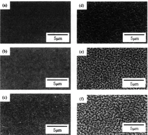
The self-assembling (or perhaps more aptly the "self-disassembling") process of surface-energy-driven dewetting in ultra-thin films is currently used to fabricate arrays of nanoscale metal catalyst islands to enable carbon nanotube and semiconductor nanowire growth and nanocrystal-based non-volatile memory applications.2 0-25 However, the lack of order and poor size uniformity of the nanoisland arrays formed via uncontrolled dewetting from polycrystalline, highly defected deposited films 22,2 3,26, as illustrated in Figure 1.7, currently limits the use of nanoparticles, nanotubes, and nanowires in novel nanodevices with new functionalities.
(a)
(b)
(c)
Figure 1.7: SEM micrographs illustrating the lack of order and size uniformity in island arrays formed via dewetting of deposited polycrystalline thin films: a.) 5nm sputtered Au film on SiO2 annealed at 700C, 15min in H2,26 b.) 2nm sputtered Ni film on SiO
2
annealed at 750C, 15min in H2,22
and c.) 1.2nm sputtered Pt film on SiO2 annealed at 700C, 60s in Ar.23
The single-crystal nature, crystalline symmetry, and anisotropic surface energies in SOI films provide ordering forces that hold promise for the fabrication of much more
ordered, uniformly sized nanoisland arrays via dewetting than has been achieved to date
in deposited highly defective polycrystalline thin films. A comparison of the highly
ordered uniform array of Si islands formed via SOI dewetting shown in Figure 1.6(a)
relative to what is seen in Figure 1.7, highlights this opportunity.
Organization of Thesis
In Chapter 2 of this thesis, we present a review of the relevant previous theoretical
and experimental literature on solid state thin-film dewetting, with an emphasis on the
work that has elucidated the kinetic mechanisms of dewetting.
In Chapter 3, we present a review of the existing literature on SOI dewetting,
summarizing key experimental observations, experimental shortcomings, and the
currently dominant perspective in the literature that SOI dewetting is a stress-driven
morphological evolution phenomenon.
In Chapter 4, we present an isotropic surface-energy-driven theory of SOI
dewetting which includes a description of both the thermodynamics of the phenomenon
and a 5-step surface-energy-driven kinetic dewetting mechanism based upon critical void
formation and void growth via two key capillary instabilities: the generalized Rayleigh
instability and the capillary film edge instability. We use this model to argue against the
dominant perspective in the SOI dewetting literature that SOI dewetting is a stress-driven
phenomenon. We also show that this model is able to account for the key experimental
observations from the literature on SOI dewetting.
In Chapter 5, we present the experimental details of our SOI dewetting study,
mesas having various in-plane edge orientations, an SOI defect study, and a
proof-of-concept of the dielectric edge coverage stabilization technique for stabilizing SOI films
against dewetting.
In Chapter 6, we present the experimental results and interpretation of the results
of our UHV annealing study in ultra-thin SOI films, including quantitative measurements
of the initial edge retraction dewetting process and the propagation rate of dewetting
propagation by void finger formation and growth. In this chapter, we also extend our
isotropic dewetting model to account for the effects of anisotropic surface energy where
necessary to interpret our experimental results.
In Chapter 7, we discuss promising avenues for future work on SOI dewetting.
In Chapter 8, we summarize this thesis work and provide closing thoughts.
In Appendix A, we briefly discuss the key anisotropic surface energy properties
of Si.
In Appendix B, we present and discuss experimental results on the effect of the
Chapter 2:
Literature Review
-
Dewetting in Thin Solid Films
In this chapter, we review the existing literature on dewetting in thin solid films.
We review the theoretical literature, with a focus on the thermodynamics of
surface-energy-driven dewetting and the dominant kinetic dewetting mechanisms that have been
proposed in the literature, with a focus on critical void formation, initial dewetting by
critical void edge thickening and retraction, and continued dewetting by thickened edge
breakdown and void finger formation and propagation. We then review the existing
experimental dewetting literature in the context of these proposed kinetic mechanisms.
The literature has identified these mechanisms as separate and incompatible. However,
we propose that they are consistent with one another, simply representing different stages
of a single dewetting process.
I. Theory Review - Solid-State Thin Film Dewettine
A. Thermodynamics of Dewetting
It has long been known that systems tend to evolve toward energy states that
lower their total surface energy. It is this thermodynamic driving force that drives a
number of well-known materials phenomena including sintering,7 Ostwald ripening,2 8
and thin film dewetting, amongst many others.
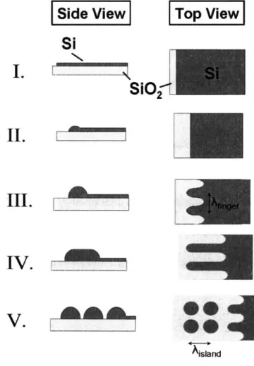
Depending on the relative interfacial energies of a thin film materials system
(assuming isotropic surface energies, no film stress, and a rigid substrate), the
characterized by the contact angle its edge makes with the substrate, as shown in Figure
2.1. Young derived from a horizontal surface tension balance at the film edge that this
equilibrium contact angle is given by
S cos-
•v-t1
,'(2.1)
vapor (v) vapor (v)
substrate (s) 7 Ysv Yfs substrate (s)
Figure 2.1: Schematic illustration of the equilibrium shape of a thin film, assuming isotropic surface energies and a rigid substrate, as determined first by Young.2 9
where ysv is the substrate-vapor surface energy density, yfv is the film-vapor surface
energy density, and yfs is the film-substrate surface energy density.2 9 If 7ys 7yrf + y7s,
then the equilibrium contact angle is zero and the equilibrium state is a flat film.
Otherwise, the equilibrium contact angle is finite and the equilibrium state of the film is
one single hemispherical island making this equilibrium angle with the substrate. (In this
work, any thin film system with a non-zero equilibrium wetting angle is considered to be
a "dewetting system".) In general, the magnitude of the equilibrium contact angle
represents the driving force for a thin film to dewet, with thin film systems with larger
contact angles having a larger driving force to dewet. The equilibrium contact angle also
Although the thermodynamic equilibrium state of any dewetting system is given
by one single island on a substrate, a range of states consisting of arrays of identical
smaller islands each making the equilibrium contact angle with the substrate are also
stable relative to a flat-film. Srolovitz and Goldiner showed that for a given film thickness,
h;, there exists a minimum island radius such that a final state consisting of an array of
islands of that radius is more stable than the flat film.30 The minimum island radius for
which such an islanded state is stable relative to the flat film is given by
3sin
- cos f. (2.2)Thus, in a dewetting system, a range of islanded film geometries are more stable
than a flat film, from a marginally more stable array of islands having radii just greater
than
rminto a single island representing the most stable final state.
B. Kinetics of Dewetting
Although thermodynamics dictates the range of final islanded states to which a
dewetting flat film can evolve, it is the specific kinetic mechanism by which a thin film
dewets that determines the islanded state to which the system will actually evolve. Here,
we describe the key existing literature describing the theory behind the kinetics of
dewetting.
Gibbs derived the expression for the excess free energy per atom at a surface
(known as the Gibbs-Thompson equation),31 leading to the following expressions for the
surface chemical potential, t(s), and surface-energy-driven atomic surface diffusion flux
Js, respectively, below:
s, = V(s)= TV C(S) (2.4)
QkT kT
where jio is the chemical potential at a flat surface, Q is the atomic volume, y is the
surface free energy density, Ds is the surface diffusivity, k is Boltzmann's constant, T is
the absolute temperature, and K(s) is the mean surface curvature at the surface coordinate
s. In this convention, the curvature of a convex surface is considered positive, while that
of a concave surface is considered negative. Thus, convex surface regions have higher
chemical potential and concave regions have lower chemical potential, driving a
surface-energy-driven atomic flux from surface "hills" to "valleys".
i.) Critical Void Formation
Mullins applied the divergence theorem to Equation 2.4 to derive an expression
for the velocity of the surface normal, Vn(s), during surface-energy-driven morphological
evolution via surface diffusion to be
V, (s) = -D V V2C(s)
=
-BVK(S), (2.5)kT
where v is the atomic surface density and all other parameters are as previously defined.32
The prefactor in this equation is a common materials constant found in dewetting theory
and will be often be referred to by the constant B going forward. (Note: Due to the fact
that curvature represents a second derivative, this equation is a fourth order partial
differential equation). Mullins solved Equation 2.5 in the small slope limit to demonstrate
theoretically that initially flat films in dewetting systems are metastable against
dewetting.33 He showed that any non-through-thickness surface morphology perturbation
pre-existence or formation of substrate-exposing voids is required for a thin film to
spontaneously dewet.33 (This makes physical sense in that any non-through-thickness
surface perturbation from a flat film introduces additional surface area and surface energy
without destroying any.) Srolovitz and Safran determined further on pure thermodynamic
grounds that not only must a substrate-exposing film void exist for dewetting to
spontaneously proceed, but that such a void must also be greater than a critical size for
subsequent continuous void growth and dewetting to be energetically favored.30 For a
truncated conical film void making the equilibrium contact angle with the substrate, their
results predict a critical void radius of
hf
rit• i (2.6)
sin OC
Under this model, subcritical substrate-exposing film voids with r < rri, will
spontaneously fill in, restoring the flat film; whereas supercritical voids with r > reit will
spontaneously grow.
Srolovitz and Safran provided further theoretical credence for this critical void
phenomenon in another paper by numerically solving for the kinetic morphological
evolution of the same truncated conical film void described above in a dewetting film in
the small slope limit (an approximation).34 They found a critical void radius value to exist
h h
between 2 - -3 h , below which their simulations showed the void to fill in and tan Oc tan Oc
restore the flat film and above which they showed spontaneous hole growth by
ii.) Initial Void Growth via Void Edge Retraction and Thickening
Two authors have proposed kinetic models for how dewetting proceeds once a
supercritical thin film void is made present in a thin film dewetting system. Brandon and
Bradshaw proposed a simple analytical model for dewetting void growth by continuous
edge thickening and retraction.35 In this model, they assumed a circular film void
geometry and that all of the mass originally contained within the void region builds up in
an edge region with a semicircular cross-section making a 900 equilibrium contact angle
at the retracting void edge, as shown in Figure 2.2.
ai NOLE PROF•tE
•mjS AREA_
S Q v /2• W2 • -
-bi PROFILE CHANGE
Figure 2.2: Schematic illustration of the analytical model for dewetting void growth via edge thickening and retraction initially posed by Brandon and Bradshaw.35
We use a derivation for void growth via edge thickening and retraction at a
straight film edge, as opposed to a circular film void edge, similar to that of Brandon and
Bradshaw in developing our own dewetting theory in Chapter 4, so we forego the
derivation here and just share the result. Using this model, Brandon and Bradshaw
derived an expression for the void radius versus time, defined as the distance between the
1 2
25= 5 B 5
(2.7)
rod
4
,
3B(2.7)
h5
where t denotes time and all other parameters are as previously defined,3 5 thus predicting
a void growth velocity, Vvoid, with the following key dependencies
2
vvoid
B
-3- (2.8)h5 t5
where t is the annealing time and all other parameters are as previously defined.
It can clearly be seen from this expression that this model predicts that the
retracting film void edge motion continuously slows down with time as the edge becomes
thicker and the curvature gradient at the edge continuously decreases. Thus, this model
predicts that dewetting at a supercritical film void should be observed to slow and
ultimately stop with sufficient annealing time.
The only other theoretical treatment of initial void growth via edge curvature
driven edge thickening and retraction was performed by Srolovitz and Safran.34 They
used the same numerical technique discussed above to attempt to model the kinetics of
supercritical void growth via edge thickening and retraction. Their modeling predicts a
rather complex dependency for the void growth velocity, valid for large void sizes and
times, of
B 43 tan
Ec
Vvoid o {7 3 Bt . (2.9)
tThe
not immediately transparent.
4is
Perhaps the most interesting result from this work by Srolovitz and Safran was the
observation in their simulation that a trough of ever increasing depth formed ahead of the
thickening dewetting void edge, as shown in Figure 2.3. They hypothesized that the
growth of a trough such as this in a real dewetting film could proceed until it reached the
substrate, allowing for the creation of a new void edge with a high edge curvature and
that the iterative process of void edge thickening and new void edge creation by leading
trough growth could allow for an apparent constant dewetting propagation rate over time
scales longer than a few pinch off cycles. In contrast with the mechanism proposed by
Brandon and Bradshaw, such a mechanism would allow for continued dewetting of a thin
film with time with an apparent constant velocity over sufficiently long times.
h
r
Figure 2.3: Schematic illustration of trough formation observed in front of a dewetting thickening void edge from the numerical kinetic simulation of Srolovitz and Safran.34
iii.) Continued Dewetting via Thickened Void Edge Breakdown and Void Finger
Formation and Propagation
The most important recent breakthrough in the theory of thin film dewetting was
made when Jiran and Thompson posed a new thin film dewetting mechanism by
breakdown along its length.3 6
,37 (We discuss and extend the Jiran-Thompson in the
context of our own theory for SOI dewetting in Chapter 4, so we only briefly describe the
model here.) Jiran and Thompson proposed that dewetting occurs via an
initial continuously slowing void edge thickening and retraction mechanism, as described
by Brandon and Bradshaw,35 followed by thickened void edge breakdown via a
generalized Rayleigh instability. Under their model, illustrated schematically in Figure
2.4, this edge breakdown results in the formation of periodic, locally-thin film edge
regions with access to a very small local edge thickness (and high local edge curvature)
given by the film thickness. Under their model, mass flows continuously away from
these local thin void edge regions to neighboring thicker regions, causing void fingers
to penetrate the slow moving thickened void edge and grow into the neighboring thin film
region at a constant, relatively fast velocity dictated only by the initial film thickness.
Under their model, the fingers of film material left between the growing void fingers then
break up via a further Rayleigh instability to form islands.36
void film oid film
(c) (d)
void film
(e) (t
Figure 2.4: Schematic illustration of the thickened edge breakdown/void finger formation and propagation model of Jiran and Thompson. 6
Assuming that these void finger tips maintain a thickness equal to the film
thickness and that mass flows quickly away from these tips, their model predicts that
these void fingers should grow at a constant velocity given by36
2 DyG2v 1 2 B
Vfinger =
2=
---2(2.10)
kT h3 hr h3
f f
II. Experimental Review - Solid-State Thin Film Dewetting
Due to the practical significance of dewetting of thin film systems for nanotube
and nanowire growth, nanocrystal-based non-volatile memory applications, and
semiconductor device layer stability, a large body of literature exists on thin film
dewetting. These studies have focused primarily on metal-on-insulator systems such as
Cu, Au, Ni, Pt, Sn, Pb, and Co on dielectric substrates such as SiO2, pyrex, and mica22
26,36-60. Nearly all of this literature has focused on the determination of the critical temperature at which dewetting occurs and on the geometrical nature of the island array
that results from dewetting, as these are the most important parameters from a purely
technological standpoint. This literature focuses only on the state of the film after
complete dewetting, and thus gives little to no direct information about the physical
mechanism by which dewetting occurs. The most important results from this literature
are that 1.) thinner films tend dewet at lower temperatures and times than thicker films
A small subset of this experimental dewetting literature has focused on revealing the basic physical mechanisms behind dewetting and quantitative measurements of
dewetting kinetics and is discussed in detail below.
A. Dewetting via Void Growth by Edge Thickening and Retraction
A few authors have observed a physical dewetting mechanism in which film voids form in initially continuous films and grow via edge thickening and retraction until the
voids impinge, creating an array of film ridges, which subsequently break up into
islands. 3 5 3 9'-476 1 Sieradzki et al. studied dewetting in evaporated Ag films on SiO2 layers
under vacuum annealing conditions.47 As shown in Figure 2.5, illustrating the early
stages of Ag film dewetting, they clearly observed the void growth via edge thickening
and retraction dewetting mechanism in a 100nm thick polycrystalline evaporated Ag film
annealed at 635C for various times. Kwon et al. studied dewetting in polycrystalline
sputtered Cu films on SiO2 layers annealed in a hydrogen ambient. As shown in Figure
2.6, they also clearly observed dewetting to occur via a void edge thickening and
retraction mechanism followed by void edge impingement to form isolated Cu islands.26
Figure 2.5: SEM micrographs showing the early stage time evolution of dewetting in a polycrystalline evaporated 100nm Ag-on-SiO2 film vacuum annealed at 635C: a.) as deposited, b.) 1 min anneal, and c.) 5
Figure 2.6: SEM images illustrating the dewetting process in a 50nm Cu film on SiO2 annealed at 300C for
various times under a hydrogen ambient at 635C: a.) as deposited, b.) 10min, c.) 20min, d.) 40min, e.) 60min, and f.) 120min. The dewetting mechanism of void growth via edge thickening and retraction and void impingement is evident.26
Brandon and Bradshaw,35 Sharma and Spitz,40-45 and Presland et al.38'39'6 1 are the only
authors who have reported quantitative kinetic studies of film dewetting by void growth
via uniform edge thickening and retraction.
Brandon and Bradshaw, who developed the model for void growth via uniform
edge thickening and retraction described above, studied dewetting in 100-270nm
evaporated Au films on mica annealed in air. As shown in Figure 2.7, they observed
dewetting via the void edge thickening and retraction mechanism. Using optical
5 5
anneals and found that plots of (rvid-fiinal vrid-initial) VS annealing time for individual voids had reasonably good linear fits, agreeing with the 2/5 power law dependence of the
void growth radius with time predicted by Brandon and Bradshaw's void growth
model.:3
Sharma and Spitz40-4 5 and Presland et al.38,39,6
1 each performed quantitative
studies of dewetting of Ag films in which they measured the exposed substrate area
versus annealing time. Sharma and Spitz studied dewetting in 50-200nm sputtered Ag
films on Pyrex in vacuum and oxygen ambients, while Presland et al. studied dewetting
of evaporated Ag films on SiO2 under only oxygen ambients. Both authors observed a
void growth by edge thickening, retraction, and impingement dewetting mechanism very
similar to that shown in Figures 2.5 and 2.6. Both authors also extracted the exposed
substrate area versus time from SEM micrographs and found that plots of exposed area to
the 5/4 power versus time for a given Ag thickness, temperature, and ambient yielded
excellent linear fits for sufficiently short annealing times that film voids had not yet
begun to overlap.38 -45'61 The growth of a collection of identically sized voids via the
Brandon and Bradshaw mechanism would be expected to result in an exposed substrate
area proportional to the square of the predicted value of rvoid given in Equation 2.7,
yielding a 4/5 power law dependence with time. This is not strictly correct, however, for
a set of growing voids having a range of radius values, as was the case in the experiments
of Sharma and Spitz and Presland et al. However, the general observation of a 4/5 power
law time dependence of the exposed area in their experiments yields further support for
the validity of the Brandon and Bradshaw model for dewetting by void growth via edge
Time: 1/2 mins. Time: 31 mins.
L~.
-Time: 8 mins. Time: 65 mins.
Scale: I /O,
Figure 2.7: Optical micrographs showing the evolution of an evaporated 1 10nm Ag film on mica annealed in air for various times sequentially. The dewetting of the film by void growth via edge thickening and retraction is evident. Brandon and Bradshaw quantified the void growth rate by tracking the radii of individual voids with time to confirm the time dependency of their void growth model.
B. Dewetting via Void Edge Breakdown and Void Finger Formation and Propagation
Two authors have observed a very different dewetting mechanism from the void
growth by void edge thickening, retraction, and impingement mechanism described in the
previous section. Kwon et al.26 and Jiran and Thompson36,37 both observed a dewetting mechanism in which the edge of growing dewetting film voids break down and continued
dewetting occurs by the formation and growth of void fingers that penetrate into the film,
shown in Figures 2.8 and 2.9. Interestingly, as shown in Figures 2.6 and 2.8, Kwon et al.
observed this void edge breakdown and void finger formation and propagation dewetting
mechanism in annealed 50nm Au films on SiO2, while observing the void growth by
uniform edge thickening and impingement mechanism in annealed 50nm Cu films on
SiO2. Comparing the two figures, it is clear that the density of void formation is much
higher in the case of Cu. We conclude that the void growth via uniform edge thickening
and retraction mechanism and the void edge breakdown and finger formation mechanism
are both fundamental to dewetting in thin films and occur in sequence when void edge
breakdown and finger formation is observed. For the results of Kwon et al., the voids in
their Cu films were simply so close together that they impinged via void growth before
they had the opportunity to break down and form void fingers. In the case of the Au films
they studied, the void density was sufficiently low to allow for uniform void growth via
uniform edge thickening and retraction to the point of edge breakdown and void finger
Figure 2.8: SEM images of 50nm Au films on SiO2 annealed in H2 at 700C for various times. a.) 5min, b.)
30min, c.) 60min, d.) 90min, e.) 120min, and f.) 150min. The thickened void edge breakdown and void finger formation and propagation mechanism is clearly seen to be active in this case.26
Jiran and Thompson also observed the thickened void edge breakdown and void
finger formation and propagation dewetting mechanism in Au films on SiO2, as
illustrated in Figure 2.9.36 However, in addition to observing this dewetting mechanism,
they also quantified the kinetics of the void finger growth dewetting mechanism in
evaporated Au films on SiO2 using a very clever technique based upon in-situ laser
transmission intensity through the dewetting film during annealing. Using a laser
wavelength at which SiO2 is transparent and Au is opaque, they were able to measure the
exposed substrate area in-situ during annealing by measuring the transmitted laser light
to study the kinetics of void growth alone, as opposed to the convolution of void
nucleation and void growth that occurs in continuous films.
Figure 2.9 contains a series of transmission optical micrographs showing the time
evolution of dewetting in their patterned Au line structures during annealing. From their
in-situ transmitted light intensity measurements, they observed a constant dewetting front
propagation velocity with time and extracted propagation velocity values for Au films
having thicknesses from 40-90nm annealed at 700, 750, and 800C. From this data, they
were able to extract both the thickness and temperature dependencies of the void finger
propagation process. They found for each annealing temperature that their propagation
velocity, Vpropagation, versus film thickness, hj, yielded good power law fits
Vpropagation hf (2.11 )
with n values of 3.4, 2.4, and 2.1 for 700C, 750C, and 800C, respectively. The
consistency of this result with the n=3 power law dependency predicted by their void
finger propagation model, expressed in Equation 2.10, supported the validity of their
model.
Figure 2.9: Optical transmission micrograph and SEM micrograph (inset) showing dewetting in a Au film on SiO2 via the thickened void edge breakdown and void finger formation and propagation mechanism, as observed by Jiran and Thompson.
50o A
B
5O Pm
C
Figure 2.10: Optical transmission micrographs from Jiran and Thompson showing the dewetting evolution of patterned Au lines on SiO2 during annealing : a.) before annealing, b.) partially dewetted, and c.) fully
dewetted. The study of patterned Au lines allowed Jiran and Thompson to specifically study the kinetics of void finger propagation in isolation, as the edges of patterned structures represent pre-existing unstable critical voids.36
Summary
In this chapter, we presented a review of the theoretical and experimental
literature on dewetting of solid-state thin films. In terms of thermodynamics, we
based upon the calculation of the equilibrium contact angle, with film systems having
finite equilibrium contact angles being thermodynamically unstable to island formation.29
The work of Mullins3 3 and Srolovitz and Safran34,62 established that in a dewetting thin
film system a flat film is indeed metastable and that a substrate-exposing film void
greater than a critical size must first be formed before the film can undergo spontaneous
dewetting. Brandon and Bradshaw3 5 developed a model for dewetting at a circular void
via uniform void edge thickening and retraction that predicts a growing void radius that
depends on the 3/5 power of time and on the -3/5 power of the film thickness, indicating
that void growth by this mechanism should continuously slow and ultimately stop. From
the results of numerical simulations of void growth via edge thickening and retraction,
Srolovitz and Safran34 observed the formation of a continuously deepening trough in
front of a thickening retracting void edge and proposed that an iterative mechanism in
which such troughs reach the substrate to create a new high curvature void edge. They
proposed that this mechanism could allow for continued dewetting at a slowing
thickening retracting void edge. Jiran and Thompson developed a model by which
dewetting proceeds by an initial uniform edge thickening and retracting step, but in which
the thickened edge then breaks down by a Rayleigh instability allowing void fingers to
form and penetrate at a constant rate into the flat film, resulting in a constant dewetting
propagation front velocity and continuous film dewetting. Their model predicts a
dewetting propagation velocity proportional to the -3 power of the film thickness.
In terms of experimental work quantifying the kinetics of dewetting, Brandon and
Bradshaw, Sharma and Spitz, and Presland et al. have confirmed the 2/5 power law
dewetting step by measuring the exposed substrate area versus time, while Jiran and
Thompson experimentally confirmed a -3 power law dependence of the dewetting
propagation rate during the phase of void finger growth after thickened void edge
breakdown. Although the literature has identified these two processes as being
incompatible and representing fundamentally different dewetting behaviors, we identify
them as simply being two successive steps in the dewetting process, with the void edge
thickening and retraction process always preceding void edge breakdown via void finger
Chapter 3:
Literature Review
-Dewetting in Silicon-on-Insulator Films
There is a significant body of previous literature on the dewetting of single-crystal
ultra-thin SOI films which has revealed a number of important experimental
dependencies of this phenomenon. (For reference, what is referred to as "dewetting" here
is frequently termed "agglomeration" in this literature). However, the current
experimental literature has a number of limitations in terms of providing an
understanding of the basic kinetics behind SOI dewetting and the development of an
accurate mechanistic model. We review the existing literature and highlight these
limitations here.
Ono et. al were the first to observe SOI dewetting in (100) and (111 )-oriented SOI
films. They performed a series 5s resistive anneals in UHV (-10-9 torr) on SIMOX SOI
samples having a top Si thickness range of 15-200nm and over a temperature range of
950-1200C. For films with thickness < 50nm, upon sufficiently high temperature
annealing < 1200C, dewetting film voids with thickened edges were observed to form
locally in initially continuous films in both (100) and (111)-oriented top Si layers, as
shown in Figure 3.1. In both the (111) and (100)-oriented samples, the voids grew by
piling material up at the thickening retracting void edge until growing voids impinged on
each other, exhibiting the previously mentioned void growth via edge thickening,
retraction, and impingement dewetting mechanism, as shown in Figure 3.2. We believe
precluded the observation of edge breakdown and void finger formation and growth. Ono
et al. observed that thicker SOI films were more stable against dewetting initiation,
requiring higher 5s-annealing-temperatures for dewetting initiation to be observed, with
films > 50nm thick found to be stable all the way up to 1200C. They also found that void
formation occurred only at defected film locations where SiO2 precipitates pushed some
distance into the SOI film from the underlying SiO2 layer, as can be seen clearly in
Figures 3.1(b) and 3.1(c).
Perhaps the most striking behavior observed in this work is the clear and distinct
anisotropic dewetting void shapes formed by dewetting in both the (111) and
(100)-oriented SOI films, as shown in the AFM images in Figures 3.1 and 3.2. In the
(111)-oriented SOI films, hexagonal voids with 3 fold symmetry (3 opposing long sides, 3
opposing short sides) having sides parallel to two distinct types of in-plane <110>
directions were formed. ((ll 1)-oriented Si has two inequivalent in-plane <110>
directions). The two types of edges were defined as <112 > -type (long sides) and
< 1 12 > -type (short sides), defined by their inward in-plane direction. As is discussed in
Appendix A, the lowest energy stable facets of silicon normally are the (111), (311),
(110), and (100) facets, with (111) or (311) typically found to be have the lowest surface
2pm
Figure 3.1 : AFM images of dewetting in SIMOX SOI samples from the work of Ono et al. a.) and b.) show dewetting void growth via edge thickening and retraction in a (111)-oriented 16nm top Si film annealed at
I 100C for 5s, while c.) shows the same behavior in a (100)-oriented 15nm top Si oriented film under the
same annealing conditions. The clear anisotropic behavior is a result of the underlying anisotropy of the surface energy of Si.1
The dominant longer <112 > -type inside void edges can facet on both a (110)
and (111) plane, while the less prominent < 1 12 >-type edges can facet on two distinct
(311) planes and a (100) plane. In the (100)-oriented SOI films, square voids were formed with sides parallel to in-plane <110> directions as well. The sidewalls of these
edges could facet on both the (111) and (311) low energy planes. The observed void
shapes can thus be understood in terms of their ability to preferentially expose the low
energy planes in Si.
Nuryadi et al. were the first to perform a more systematic study of SOI dewetting.
They were the first to clearly illuminate that SOI dewetting kinetics and the resultant Si
island geometries are completely determined by the SOI top Si layer thickness and were
the first to observe the thickened void edge breakdown and void finger formation and