Designs for Ultra-High Efficiency Grid-Connected Power
Conversion
by
Brandon J. Pierquet
S.M., Massachusetts Institute of Technology (2006)
B.S., University of Wisconsin-Madison (2004)
Submitted to the Department of Electrical Engineering and Computer Science
in partial fulfillment of the requirements for the degree of
Doctor of Philosophy
at the
MASSACHUSETTS INSTITUTE OF TECHNOLOGY
June 2011
@
Massachusetts Institute of Technology MMXI. All rights reserved.
Author ...
...
Department of Electrical En
ee'ng and Computer Science
May 17, 2011
Certified by...
.. .V.- .. ' .f .. .. . ... ... . . . . .
Professor David J. Perreault
Department of Electrical Engineering and Computer Science
Thesis Supervisor
Accepted by...-.
-.
-....
P fssor
s i A. Kolodziejski
Department of Electrical Enginee
g and Computer Science
Chairperson, Department Committee on Graduate Students
MASSACHUSETTS INSTITUTE OF TECHNOLOGY
JUN 17 2011
LIBRARIES
Designs for Ultra-High Efficiency Grid-Connected Power Conversion
by
Brandon J. Pierquet
Submitted to the Department of Electrical Engineering and Computer Science
on May 17, 2011, in partial fulfillment of the
requirements for the degree of
Doctor of Philosophy
Abstract
Grid connected power conversion is an absolutely critical component of many established
and developing industries, such as information technology, telecommunications, renewable
power generation (e.g. photovoltaic and wind), even down to consumer electronics. There is
an ever present demand to reduce the volume and cost, while increasing converter efficiency
and performance. Reducing the losses associated with energy conversion to and from the
grid can be accomplished through the use of new circuit topologies, enhanced control
meth-ods, and optimized energy storage. The thesis outlines the development of foundational
methods and architectures for improving the efficiency of these converters, and allowing the
improvements to be scaled with future advances in semiconductor and passive component
technologies.
The work is presented in application to module integrated converters (MICs), often called
micro-inverters. These converters have been under rapid development for single-phase
grid-tied photovoltaic applications. The capacitive energy storage implementation for the
double-line-frequency power variation represents a differentiating factor among existing designs,
and this thesis introduces a new topology that places the energy storage block in a
series-connected path with the line interface.
This design provides independent control over
the capacitor voltage, soft-switching for all semiconductor devices, and full four-quadrant
operation with the grid.
Thesis Supervisor: Professor David J. Perreault
Acknowledgments
Firstly, and without a doubt, most importantly, I must thank my research advisor Dave
Perreault. I have had the pleasure of working with him since I started at MIT, and could
not have asked for a better mentor. Over these past seven years, he has selflessly shared his
humor, knowledge and extensive experience, for which I am a better engineer and person.
Robert and Bill have been two of the best colleagues and friends that I could wish for. They
have been present since the beginning of this expedition, which has been filled with both
dark and bright times. I owe both so much more than can be expressed here. With the
inclusion of Brienne, Brooke, Nikolai, and Cara, I consider all of them family.
All other LEES students, both past and present, that have made the line between work
and fun often indistinguishable. The open sharing of ideas and vast expertise is something
I have rarely found outside of our humble basement, and it will be sorely missed.
There are too many other people to name that have been a part of my time at MIT. some
have come and gone along the way, and others that were here when I arrived are still here
as I leave. Those that have helped me know who they are, and how grateful I am.
A substantial portion of the funding for this research came from the generous support of
Enphase Energy. Their interest in the outcome of this work has been extremely motivating,
as has been their tolerance for the twists, turns, and dead-ends that plague this type of
work.
And finally, I thank you, the reader, for your interest in this thesis. I sincerely hope that
you find the information contained within to be worthy of your time.
-5-Contents
7
List of Figure11
Lt r 'FIWesLabl
I
17
1IntroducHtion
9
t~~~~~~l~
~
K i5l! o fh ,j
.. .. . .. .. . . .
20
1L
(A c m
. . . .-
.
-
.
-
.
-
.
- -
23
. .
21
T !" i
b
(
A
.
l
A
.
. . . . .
- - -
.
- - - -
.
-
.
-
. .
29
2
C
onv ertrOperat
0 i1o
and Control
31
12. L tl11 1Ii( I... ... ... ... ... 31
.2
i Nb -I .... .. . . . . - . . . . . . . . . . - - - ...31
2. 1 A m '1 -6 r Ami...a... ... 32 2 '.'2 . . . . . - .- - - .- . . . . . 3 11
. . . .
32
[,m
m
lo
l
. . . .
- -
.
-
.
- - - - -
. . .
-
. .
36
38
I... . . . ...
40
44
2.1 \V e 1formj1 Prc( )1. ... ... ... 52
2.5 T inin Param ee Se tion .... .. .. . 56
2.75.1 Path IDinition.. ... 57
2.52
f' Fimi ing. ... 593
Prototype Design
iand Verification
65
;i. I n rod uc io . . . . . 65:S.2 It ere
n t
kil Imentt ion . . . . 65:3.: Te
tin M e hod log
. . . .
69
:;.1 1
Stati M
eas
enwur
. . . .
6
:
f3.
D v o Ic
e
s r m
. . . .
70
:),,
E xperimetal
I
su
t
. . . .
-
. .
71
.T
o
e
m
m
. . . .
-
.
- - - -
8
4
MulIti-PIase G'id Inter1face
85
4.1 In o u..i... . . . . . . . . . . . . . . . - . . . . . . - . . . .. .. .. .. 851.2 Dalan id Th m Phas (Operaution . . . . . . . . . . . . . . . . . . . . . . . . 85
4
Pow r M< n iNo n . . . .
88
4.4 fF ecti vf Lt tm.me . . . . . . . . . . . . . . . . . . . - - . . . . . . . 90
1.5
Sinlm
hl(a
R
ults
. . . .
.
.
. . .
.
. .94
L.
C I tus (I
t
. . . .
96
5 Thesis
(onc
iision s 99 5. Su mnovI I... . . . . . . . . . . . . . .. . . . . . . . . . . . . . . . . . .. . .. .99A
(
onverf-pt er Sdchematics. Bill-of-Materials,
andA ,
1)i~l "I k a~terials
. . . .
. r i . . . .
B.
C norw
Simo
Hio
. . . .
he pvmi /c nur itrset
epu mi corve-rte ro per ati
hie pvi/f pgac orep
. . .
hepvmi / ideal zvs py
. . .
hepvmni/ init py . . . . hepm-i /parameterestimatgex tact-ps.py ...
gen seaepist.py . . . .
.
cloadsaveng .
. . . .
mosfet parmetersJy. tt iep a v . . . . . . . . . sc\\
\I
Ij, HiII IHlPCB
io n. p y on. py . I ,n . . .1 . .1 .9-CONTENTS
F;
I;
I'IL
I F
I;
Ii~
Cj Digitatl
Co
I
>(M C 2 ( Li . . . . . 146153
153
153
155
155
101
101
103
115
119
119
119
121
123
129
131
135
135
137
141
144
144
145
.. . . .
. . .
-. -. -. -. -. -. -. -. -. -.
. . . .
(C.1.41
C 1.
-C.1.7
(C.1.
~
C.I.9)
input protocol decode.v
..
pwm
root
controller.v . . . .
serial
async receiver.v . .
serial async transmitter.v
serial-to.
set reset
pWm.v . . .
.m. en- v1 U p,(.)
spi slave.v
(. LI (2
M ir(.2.1
C
.2.i
C
.28
C.241
sync
fifo.v
oit e1t'r Itip
dac.c . . . .
dac h . . . .
leds.c
. . .
leds.h
. . .
main.
c
. . .
spi-adc.c.
spi
adc.h.
spi-fpga.c
spi fpga.husart.c
usart.h
ii it ai II157
160
163
165
167
171
173
175
177
177
178
178
180
180
197
199
199
203
203
210
213
D BibliographyList of Figures
- a Aa ,( t a! la al at m w-a tla aitt- w ia all l pmmF ho a'(dk l alT
K! 1W UkI1T(W"Wa N l TPlIVU nwitm N a -
-1 4 G itko- m m m 1 ii it m ' &t hal '1.1' i -'til ow rg l t' Ilk Ha I''ata pt'
>
01 e
li IM )M I IM I 11. 0 h -CC
IC idL a a 1 all t ilk a 11 it A i a T' ( a a'C Ol HI pr int . -- gAl.IT
a ai aill a0 aC aT 1a-P- 1 11 W
(apla - 'a al1a a nd T 1 VI i ) > 0,111 0 41 a, III S11 a 1 i( a L l l u aa -1 al a - T L w . . . .. . . . - - - .
aS ad all Itv m a aV ii atc.( Il Ia! awi ) l w r ) n tn 1'a), &
in i l .ll aa a . . . ad a .a . .' .... a a a a. [ T...()... ) a Sa 't a n b) a I l l . a riwASWi .- I ta a a a .I a at . . Im 1 ( NTIM P lil to . 1 0
ll'J aAt l a a (It t i ita
a) a aa )O1 m a t ics' a aa 'IM -Si Hi
- 'Q a -- I - -It - -a- a Wl atmv a a.ti
2
Th1
. . . .
- .
- 11 --i lilita ohna F'25
Tlie inniliiiu
reoanlut'ent nimiigilitiideo reclitires for tlle bitfer-block imd
iiie-~nne~eel CelCOI~ertl r
iltinliedt. with1
0li
bld
linex repre'seiting"
the
couibinedl
ltinnunn ue
m
v~nt en
.o .. . . .
42
2.(
tlie pliase
eAtiisilpsoforte
CyclowRl\TTeandt
ANYf
WRI
lekitn
Oqated i ln ph hi4 mI(I lub t in. . . . . . . . . . . . . . . . . . . . . . . 44
2
7Itile
nornmiIZed CmlipleX ilnpedairet oftht,
bliffei-bleek
antd
c
ylocomvytfqrare " l4wn lo v1 ry v a 1 li ( I' tl a d }(}4 t141 lii i n m Or 111 li li I
-C'r11r' ilt driVe4 iltilod. Bol li (' 4 111I 1 uiitiLd pl' a 11(t 1) m444 444nt1
relat ioni sI lre prese ll d . . . . . 45 2
Iil
llor1'a1 lized lo di(l i 1pedliie' p '4itnted to f4i1
full-bridgen4iv r >v ( a) ,I )he w oucer->lock. an< WyDcnea gs a< mm gtesre
r s1onlt tank. Witlhou1t 1h
iili
1(1ta4144of It' 1 e. iit of ORik, LHie re(tahitpre4en41 to the owiuver prvens zeovon'w n . . . .. . . . . . 46
2.9 4T1
1(is
buffeb4-1ock 44 ivrr L( eb4n1ari in (u) is apprxii4a44 dusing14pha4-sors
(ttli, ,,witclhillg
fr(WpltwC)
inl(1)).
faclh
:'witcillig
)(>k
is
a~rx
inlmlel
by atua
asourceo.
mnd
a1
(
anplex
impet
moevinl
ph~weOFf
thtranisforma1
tion
t a
y
. . . .
47
2.10 A
imiltiph-iinpu it h ipk-ong u moildl For ilhe
c-Onverlter1
(ktut rol)
. . . .
49
2.
ilt~llT pli. 71 W \lle
v id slut-ioillsots of
rtwo
powel
rnsfT(>ev f
jl4ver t 1 (4, 1;, Oc) '
11
1 we. 11he iLi'erse(i n-)F41
it' I wN w ( vnt ur ;ith1
"'4t o s(o1lution4 thlt 11 ot ' 1) ith '1 1ws1 . . . . . . . . . . . . . 50
2. 2 A a of va41d so441ion' Or vary mL 14a44n4 44444 ' ) w NNitchig4 frequ w'y
an1( fll-bride. in4verter dty-rtio. Tm 'iller blu point s intd'iNOt
41w4
(Calclatedt for ["G1=1 01 W.t=7[.[=3V
(=V
ivn
,
(onver' r ma414hn 1 4 wp fi4o n4' ' in TA M [14 .2.1 . . . . 51
2. 1 :1 ulti1ple soluition maps
create,(d
th ow
the ra
sof
a)pplied teria
ages, an
lw cons1tints ofI desired >ow"er rnse
constraiwinti
aunm
thw
thIree po rts results
in1 1 I uiIt i< inwI n ' siol o s t1 pao f val Iid cou IverltIer, qoperatogI
pa rn norAm
. . . .
52
2 4 A
compaurison
of 1he
ca
aoed
linit-iffereu
ne weform soH
wnl
mn->llred
ill-A
iri
walvceriils frit monveThi
matebtlig,t,
pefiain
ill
Ta_W)( :3.2 (open"W
"ii t h ,=20 W
=70V32
.
15; = (I - . A I= P, J . f =I8 k[)IZ. e 6 2 Io 2 11 7 . .. . .. . . . . 56
it1
e1" pornti a NI Am o& [at th oeltA i imn k ()iq I lb01 o Ft (A Ieetz (TnaLIST OF FIGURES
2.th1
0
wSto
m- sts> asi1Ate Nd l ithr , path ill Fig. :2.17. 0or
y
ilbstrating
het
sil;ap
) l,;llQlQf)1>tile
aisms()lI
arhi
()mlYin Djstr, tolem
Illenssdsnt
t
ts
ts'In t KU 2A
l\
. . . . . . . . .60
i7
I
Itt
Im genwv tito
1
o tir n w,)ie tvr
lie
11111w...it 1 tip he 51 we.re.s.-uant cii it ti tiin! io u ln m at iaih I tI . ITh h i n it m ex I i
harp
2r
a i iS i li vari 0 >e n ar- 1711 \ . . . . . . . . . . . . . . . 6112.0
heto:
ecpifst
asIso-ciand wIthtlw, path in
Fig,2. M. Hlltmtiy An 1the11
i114 hlow
cost
s
nps fomei byv the Dijk~sl
A
ig
rrlu.
..
. . . .
62
The9
'11P W
reted
forIrien
tinor;t
inu y,v.
W
hrcland
onumrii ciu rmaw iiim i it I w< rquirmnent (ioml Iue wit i I . 2.17. T a iSo utionimiaek
rw
p i
tu-
dw
r Iu
iraniti ons..
. . . .
63
joo;, tu
nt inining waurnantIbes
and digiadmorol
bonnL. . .
67
we2t
Pcmmu
iri toplo~gy
fOrthle
prmtotype
evaluatedo
ill thin Qhqpr,
. .
67
111stt In -- Ifw q tp in d al 1i aslurk . a, tic buit lid k of wi ll ik ui 1 m inkll
k hr I uq pn we 10 .ig a w a . . . . . . . . . . . . . . . 70
T
straviton
ofthlm
dyNmnil (W1 lmv>ntfarnT Votp.
O)nlydw hin
uwa
om11"t pm po - ;m suplj It i ll Im msure as.ti i beI mf i e dmk st (AuHeimrge
in amuim
byi
thp,
w-4tm uat
ret-vd. . . ..
. . . .
71
pwjomy jw nw~m v Or R.,
1-35)(Y
CH
CV&"vH>
neT
. . . ..
b
owk.
CHI: (vWto
v(rt(-[H
p '
10H
pa w
I(
l
T1
1 1
\,
Hi
11
H A4: %q1 vaiN
IVI0
W\ 32
\7
I .\
W . .. 170 -,2 \\2
. 1 7tt \ t .t . . . ...I Pit
N
)r ti4 tt otw* i it ith I iW'
t1,i
3.9 Switciing freinlicy for the stati( d-d, operatig pons p
27;
fromig .1 Theptst'- correspondl to the input votg+of 2.5 V (top). 3'2 V (iiddle). aind 10 V
(bottom). lor I (teps
wr
a d <p er oiN-e'vle. in five pol ertv.'.
. 753. 1
)FiiH >ridge imnvete(ucv-W howr
the
static
d.41c operaingpodints
roml Ii g. -.8 T i pl ts ri tii t e11 input voltags of 2V (top). :32 V(mil
AN
. au 41V
(boHtomfor
1tsa
mer awv.; quart 1, line-eyce,
Il
anive
po er l vels
. . . .
76
1
116uferbock
andetC velconerte phase-shift values for thte static de(-de(
oper-, t i pin from Fig. 4,1The plots correspond to thei i -ItmIgte powerl. letvelsof 40 W.
GW.V
H00 W.
1~>0\
and 200) W. Cor 14 stcps ove a
wartr
line(-cvcle, and1 thl-tr inpt vlta- ('in I 'ih p o.t ti' *vll ouvtrt e iliir da11It arlprNsel N i v Hw, dhedl tin. wil It (fe -tlock datai est at
t
olid i nes. 773.12 Constant input ryow bieymk SiHnusia outsH IUower (reAlm00
Didrci im>ffer1- >loc [Tower trolaferl (g ; .agenta ) . . . . 78
1.13
A
unilriplet-iniput
umiltiple-ut
put modeld
for ti, conrier
cmld.
irA i l
fe d f r a d lfo kalp
tdthk
. . . .
79
Vene Pr nrmmHi n g int o; an Im inIeR. wvim =I
\V t
1=2
V.1I
070
\.The vefrn
are
CHIm I- II -1: 1 ZesoutI I1.7 Cur Vrent. C 1-2: Fnl
Br1 idge.
CH
T
3:
17f0-B c .CH4:
Qca
wm rter
. . . .
80
:115
En mmn Qof atjj Vr-rSsing IrIn qI Ilemm whnin Fig.:3.
14.foV I
Q
series-bu11ffer bl, c k1 pmttp
coi 1 , 1n Itr1-(r ruannitng int a0(IIn a",-Iinew. wvit III
ts=
,
INV
C
,
3
.I
-570
\ TI'il wmveforing
t( ('11: Post
llan(
rt
I~nt.
(1
:WFull
Bridg.
CHI: BuA r-Bloc.
CH14: Crelemonveter.
. . . .
81
*1m T1hinpu 1AdOi omII pu. vobag onU entrenE wiveforms, lor theiobu r1-,,z,7(h
V.=2I4
,
P
Twwave
onusarc
CHi:
Tutim
Curamn("1-2:
Onrputy Cuarrent. CHI: Inpult Volm.
CHit: DUn-ipt Volt..
. . . .
82
4.I
A
I ()l-hit
ouput
leresole (oneter
iMust raold
u1sing (a1)
anlex-morivm tranorimer
t
b
ene
npurpluls: (W
n
cnial switch unaesr
forw
ipl ing
t
w e od> int
ha)
2.
. . . .
86
't ivree
me yo aewanOrms.
jjtw, wrIQ ilnusjil iS symaNqQ
by2z A
LIST OF FIGURES
Y",w ormabard switchingL lunhi-Wd no m "all with ('l) 11
4 4
Ir I(114 l W1 11444w1 11 1 40 |)H 1 c . K(ljil
.11i on4 . n t d j enitws ti[ e r1m' t fr
r
I Io
tiInv
1e
1
1114. 41 1 141 -' . . .. Q I It-l i ll T . j(- f I W A 114 I i1 44 11. b 1 1 d m oi (1p .. . . "41111, [.44 4. . .4441 TM y Vn . .. . . . . . . . . 1 r . . . . . . . . . .t
)n
j r
W
T.
. . . .
.
1p) . . . . . .. Borrou Wiw:opwr W3) lqwi . . ..
j ol (W p r , ) 11ye'r . . . . . . . Baown sede masklaver . . . . Bot n lsikl,
re n wne.
. . . . 14 e '4 of t i4l4.4o u sI'o
) 141 k '4 1 111 1 1) l. . . . . . . . . . Tx
ne lse. . . . . 144 p1 op i ) ye .. . . . . . . . .. BA1m
a n m o !2) r.. . . . . \< 114 1 11 w -' iig W * 4 Amm.'
i 4) u' r14') m mgh 1 h , 1r "' IN A 1wit nn11 m11 41 . . 1. Nw10
-p11a11- p- 0
t
sJ i
. .
.d
d
.!"
. .h. . . ..
. . ..
.
.
.
.
.
.
.
.
.
.
.
.
.
.
..
10
4
.
.
.
.
.
.
.
.
.
.
.
.
.
.
.
..
10
5
.
.
.
.
.
.
.
.
.
.
.
.
.
.
.
..
10
6
.
.
.
.
.
.
.
.
.
.
.
.
.
.
.
..
10
7
.
.
.
.
.
.
.
.
.
.
.
.
.
.
.
..
10
8
.
.
.
.
.
.
.
.
.
.
.
.
.
.
.
..
10
9
.
.
.
.
.
.
.
.
.
.
.
.
.
.
.
.
.
110
. . . .
111
.
.
.
.
.
.
.
.
.
.
.
.
.
.
.
.
.
112
.
.
.
.
.
.
.
.
.
.
.
.
.
.
.
.
.
113
.
.
.
.
.
.
.
.
.
.
.
.
.
.
.
.
.
114
plan
i rl L . . . . . . . . 116.
.
.
-
.
.
.
.
.
.
.
.
.
.
.
.
.
117
.
.
.
.
.
.
.
.
.
.
.
.
.
.
.
.
.
117
.
.
.
.
.
.
.
.
.
.
.
.
.
.
.
.
.
117
89
91
444 4.4 A. IA.2
\A A,A.4
A47 A. 11A . 1
A 1
A. -1
.
.
. .
.
.
. .
.
.
. -
117
A 1
~ ~
M m qw IQ W te 11ire,
i l . . . . .C)pcira
ino mn
,i au
(sti
tie
t
liqi b
w p
r
f-tl (y
ptI t 11live'rN
1w A t , 1 t a4
f
f IsIhl Ip I i C id l i(1 atit'
Iih ,i r f tit . .~ . .. . .I . .IL) . . .I .t .il . .i .i .t . .
li
. .ii .lit . . . .103
-17List of Tables
ii sill if[[&Iw)
!iil ) ;
Chapter 1
Introduction
1.1
Background
Initial use of power from the alternating current electricity distribution system was focused
on automating machinery and providing lighting. While the basic applications are still
in use a century later (albeit more refined), they've been increasingly replaced by more
advanced implementations, or alternatives that don't utilize AC natively. Instead, modern
grid connected machines and devices convert the grid voltage it to a more appropriate form
such as DC or high-frequency modulated AC. Additionally, much of the electricity used
today is in residential and commercial environments, a shift from the primarily industrial
usage a century ago. This document focuses on electrical systems from the perspective of
grid connected electronics, specifically photovoltaic inverter systems.
Connecting electronic devices to the AC distribution system is a well understood task,
and significant work has been completed in both sourcing power from, and delivering power
to the grid
[
-
].
Much of this work is focused on three-phase interconnection of varying line
voltages, with power levels ranging from 10-500 kW, often for applications such as motor
drives
[
,
],
electric vehicle drivetrains
[],
wind turbines
[
,
],
and UPS systems
[
,
].
In contrast to these existing high-power multiphase systems, the electrical systems found
in commercial and residential environments often operate on a single or split-phase interface
at a significantly lower power level. Renewed focus on energy efficiency and small-scale
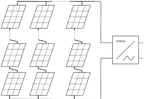
-Figure 1.1: A centralized-inverter topology converts dc-power from parallel-strings of
series-connected solar modules to grid-series-connected ac power.
distributed generation has created a demand for more effective solutions in a number of
areas. One of these areas, which is the central area of application for this thesis, is scalable
residential and commercial photovoltaic energy conversion.
1.1.1
Photovoltaic Installation Types
Grid-tied inverters for photovoltaic systems represent a rapidly developing area.
Tradition-ally, installations use series-connected into modules info strings to increase voltage, with
parallel sets of strings used to increase the output power. These arrays, as illustrated in
Fig. 1 1 are interfaced to a single dc-ac inverter, as the single inverter can be optimized for
a fixed-size array. Typical utility scale installations may exceed 1 MW, whereas medium
and small commercial rooftop installations may range from 75-250 kW.
1.1
Background
As centralized inverters have evolved to support smaller installation sizes, micro-inverters,
also known as module-integrated converters (MICs), have been developed to interface a
sin-gle, low-voltage (25-50 v, typically) panel to the AC grid
[
-
]. Micro-inverters provide
a number of system benefits: array redundancy and scalability, ease of installation, and
increased performance in partially shaded conditions
[
].
Notable drawbacks are the
du-plication of components (enclosures, control circuits, etc), and the difficulty in obtaining
the same efficiencies as inverters which manage multiple series-connected modules at higher
power levels. A single 72-cell panel, with a nominal output voltage of 36 V, requires a much
larger transformation ratio to interface with a grid voltage of 240 V than a series string of
10 modules requires.
1.1.2
Single Phase Challenges
The grid interconnection most commonly available in residential and small commercial
systems is single phase ac (e.g. at 120, 208, or 240 Vrms). Module integrated converters
typically target these electrical systems
[ ],
however one large challenge for these single
phase converters is the sinusoidally varying power transfer to the grid. The constant power
output of a solar module is poorly matched to this time varying requirement, as is shown in
Fig. I.2, where the gray shaded areas illustrate the energy storage required to compensate
for the instantaneous power mismatch.
The flow of power through the converter can be modeled as a three port system such
as the one in Fig. I.
Power flow must be managed between each port, with the fixed
requirements of maintaining dc plus twice-line-frequency sinusoidal power flow with grid,
and constant power draw from the solar module. The input and output power transfers can
be described by
-Power Mismatch Between PV Panel and Grid
Pavg
0 7r/2 - 37r/2
Line Phase [rad]
Figure 1.2: The power flow mismatch between the grid and a
in the shaded area, representing the required energy storage.
Ppv
= -- Pavg,PLine = Pavg(1 - cos(2w1
t)),
constant power source results
(1.1)
(1.2)
and the power transfer of the energy storage buffer is determined by the difference in power
between these two ports, specifically
PBuf = Pavg cos(2wit).
(1.3)
The absolute minimum required energy storage for buffering the power transfer mismatch
is the summation of power transferred into, or out of, the buffer over one-half of a line cycle.
Integrating (1.2) yields
Pgrid
/ panel 2Pav
1.1
Background
PV
+
Single-Phase
Line
IL
Inverter
Buffer
Figure 1.3: The generalization of a grid-connected power converter as a three-port system.
Wmin - Pavg
(1.4)
WI
which represents the lower bound on the energy storage required by the converter to
prop-erly manage the power flow in the converter. This, however, does not account for further
constraints imposed by the converter implementation, or more specifically the circuit
topol-ogy.
1.1.3
Existing Topologies
For single-phase module-integrated converters, past literature reviews have investigated a
comprehensive set of micro-inverters designs below 500 W
[
,
],
and classified them into
categories based on their number and type of their power conversion stages. Here, three
types of converters are outlined, however, they are categorized by the location and operation
of the energy storage within the converter.
Most single-stage topologies, such as the flyback and ac-link converters, place capacitance
in parallel with the input [
, ].
This is an effective low-complexity implementation, but
in order to avoid interfering with the peak-power tracking efficiency, substantial energy
-Vac
Vdc +
DC Link
Flyback
Unfolding Bridge
Figure 1.4: Grid-connected inverter with primary energy storage located across the input
source. Implemented using a flyback converter and unfolding bridge.
storage is required to keep the voltage ripple extremely low across the panel. A common
second method involves two cascaded conversion stages, providing energy storage at an
intermediate dc bus. This arrangement can be implemented with less energy storage than
the previous method, as a much larger voltage fluctuation on the intermediate bus can
be tolerated. Additionally, recent work has investigated alternate "third-port" topologies
(e.g. [
,
]), which can control the voltage on the energy storage capacitor independent
of the input and output voltages; the series-buffer-block converter presented in Chapter 2
belongs to this category.
The first converter topology considered places the energy storage buffer across the low
voltage dc port, in parallel with the PV panel. This type of connection has a
signifi-cant energy storage requirement, as fluctuation of the voltage across the panel impacts
the peak-power tracking effectiveness of the converter, reducing system efficiency. The
conversion from the low-voltage dc can be accomplished with a number of combinations of
high-frequency inverters and rectification schemes, such as the flyback converter followed by
an unfolding stage shown in Fig. t 1, or a single-stage ac-link structure with cycloconverter
output
[
I
(not shown). Due to the location of the energy storage, the entire converter
must process the full range of power into the line
(e.g.
0
-
2Pavg).
1.1
Background
Vac
Vdc
+
Boost
DC Link
Inverter
Figure 1.5: Grid-connected inverters with an intermediate DC bus for primary energy
storage. Implemented using a boost stage to feed the DC bus, and a full-bridge inverter
across the line.
dc port and the line interface through the use of a shared intermediate dc bus. A dc-dc
boost stage operates to isolate (if necessary), and scale the voltage up to the high-voltage
bus, which is held within a voltage range above the peak of the ac line voltage. Interfacing
to this intermediate dc bus to the line then is performed by a dc-ac converter, either in
the form of a full-bridge inverter, as shown in Fig.
,
or using a buck converter with an
unfolding bridge. In this topology, the second stage is required to process up to double
the average power, however the first stage only needs to convert the constant power output
from the panel.
A number of alternative topologies decouple the energy storage from both the input
and output stages of the converter, using a actively controlled "third-port". Two of these
topologies
[
,
],
shown in Fig.
,
implement the storage port as a separate branch that
is in parallel to the line and PV ports. This additional port is controlled to allow the
capacitor voltage to vary independently from the input and output voltages, which can
permit a substantial reduction in the energy storage compared to the topologies in Figs. I
and !.
-Vdc
Vdc
-Figure 1.6: Grid-connected inverters
Implemented using an isolated ac-link
current-fed converter
[
I.
with a third port for primary energy storage. (a)
structure
[
],
and (b) implemented as a non-isolated
Cbuf
1.2
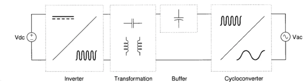
Series-Buffer-Block Converter Topology
Vdc Vac
Inverter Transformation Buffer Cycloconverter
Figure 1.7: Block diagram of the series-buffer-block converter, illustrating the single-port
nature of the buffer.
Vac
Figure
in Fig.
Inverter Transformation Buffer Cycloconverter
1.8: Schematic of proposed PV micro inverter, corresponding to the block diagram
.7.
1.2
Series-Buffer-Block Converter Topology
An additional third-port topology, which is the primary focus of this thesis, has been
de-veloped that places the energy storage in series with the input and output ports instead
of parallel as in Fig. 1.6. The high-level block diagram and the schematic of the proposed
converter are presented in Figs. 1 and L.
The dc-connected inverter transforms the dc
source into high frequency ac, with the transformation stage providing both voltage gain and
appropriate impedance shaping. The cycloconverter is controlled to modulate the transfer
of the high frequency resonant current in response to the changing voltage of the ac port;
the buffer-block acts in a similar manner, but is controlled to absorb or deliver power to
the storage port to compensates for the power mismatch between the dc and ac ports.
The proposed topology in Fig. 1 contains four low-voltage devices for the full-bridge
inverter, four high-voltage devices for the bi-directional half-bridge cycloconverter, and two
additional high-voltage devices for the half-bridge series buffer. The half-bridge buffer is
positioned on the secondary side of the transformation stage, which substantially reduces
the volt-second magnitude imposed on the transformer, and permits use of the higher energy
density of high-voltage capacitors in the buffer. Alternatively, if improved energy storage
and semiconductor devices are available at lower voltages, the buffer-block can be placed
on the primary side of the transformer.
In comparison to existing designs outlined in Section
1. 1,
including the third-port
topologies, this topology effectively places all major power processing blocks, (e.g. the
high-frequency inverter, buffer-block, and cycloconverter) in a series path with respect to
the high-frequency resonant current. This allows the power-flow to be modulated in each
block by controlling the switching function relative to the current.
The placement of each block in series with the drive current seems, at first glance, to
impose a heavy conduction loss penalty. However, the proposed approach provides means
to mitigate this loss, in addition to presenting opportunities not found in previous designs.
Using unipolar devices such as MOSFETs, and implementing zero-voltage switching (ZVS)
for the primary switches, allows the semiconductor area to be scaled up to reduce conduction
loss
[ ].
Devices such as IGBTs, SCRs, and diodes operate with a fixed on-state voltage
drop, an intrinsic property of the p-n junction, which does not scale with device area.
MOSFET device figure-of-merit values have improved steadily since their introduction,
and the recent use of charge-compensation principles has allowed high-voltage silicon
MOS-FETs to surpass the "silicon limit"
[
-
)
and become viable for voltage ranges once
relegated to IGBT devices alone. Additionally, the emergence of wibandgap based
de-vices, implemented in SiC and GaN, have the potential to dramatically reduce the on-state
1.3
Thesis Objectives and Organization
resistance of devices even further while reducing undesirable parasitics
[
,
].
This
his-torical semiconductor device progress, combined with these and other anticipated future
improvements, are a motivating factor in the elimination of p-n junction devices with this
topology development.
1.3
Thesis Objectives and Organization
The primary objective of this thesis is to develop a method for implementing a high-efficiency
grid-tied power converter, using the unexplored circuit topology of Fig. 1 ., including the
control methods for single-phase grid interconnection. Additional functional goals for the
operation of the converter include
" Independent control of the power buffering, allowing variable-voltage energy storage,
" Stable and controllable over wide input and output voltages, and output power levels,
" Bi-directional power transfer, including reactive power transfer capability,
" Scalability to future semiconductor device technology, voltage levels, and power
re-quirements.
Following this introductory chapter, Chapter 2 develops the converter model,
operat-ing fundamentals, and control methodology. A proof-of-concept prototype is presented in
Chapter
',demonstrating the converter operation and performance results for single-phase
operation. Chapter i presents a variation of the converter topology, as applied to a
three-phase grid interface. The thesis is concluded in Chapter 7 with remarks on possible areas
for future development.
-The appendices which follow the thesis include associated derivations referenced in the
text, the developed computer codes used for converter simulation, the printed circuit board
artwork, and digital controller implementation details.
Chapter 2
Converter Operation and Control
2.1
Introduction
In the general form, operation of the converter requires control over the switching functions
of each block relative to others. The combined voltage pattern of all active blocks, imposed
on the transformation stage, is responsible for generating the resonant current that links
the converter. In turn, the switching pattern of each block relative to this resonant current
is what determines the average power delivery for that block. This results in a
tightly-coupled non-linear relationship between the output voltage waveform of each block and
their respective power deliveries.
To approach the control of the converter, given this initial complexity, it is broken down
into a common switching sub-circuit, which is then analyzed and used to construct a
general-ized model of the converter operation. This model is then used to illustrate the development
of the system control methods and a functional prototype design.
2.2
System Modeling
At the outset of the analysis, two reasonable assumptions are made about the converter's
operation:
-1. The voltage at each terminal of the converter (PV, buffer, and line) changes slowly
enough, relative to the switching frequency, that they can be approximated as constant
over a switching cycle. This effectively decouples the high-frequency switching model
of the converter from the low-frequency power transfer model used over a line cycle.
2. The quality factor of the series resonant circuit is sufficiently high to approximate it
as a sinusoidal current source operating at the switching frequency. This offers the
opportunity to use of phasor analysis, and calculate equivalent impedances.
2.2.1
Power Transfer Modulation
The modulation of power through the blocks of the converter is accomplished by controlling
the switching function of each block relative to the series resonant current. To quantify this
operation, the canonical switching module of the converter is used for illustration. In its
most general form, the canonical switch model shown in Fig. 21
is composed of a single
pole, and two throws. A voltage source
Vt
is placed across the throws, and a current
source 1, is connected between the pole and a single throw. The operation of the
three-terminal switch prevents an open-circuit of the current source, and the short-circuit of the
voltage source. The operation of the three-terminal switch can also be implemented with
two complimentary operated two-terminal switches, as shown in Fig. 2i b. For purposes of
this analysis, we ignore the details of the switching transitions, including means providing
zero-voltage switching in the actual converter.
The modulation of power between the current and voltage sources is determined by the
values of these sources, and the function
Q
controlling the switch operation. The current
in this switching module represents the resonant current through the converter, and the
voltage source as one of the terminal voltages (e.g. cycloconverter or buffer-block), which
can be written as
2.2
System Modeling
(a) (b)
Figure 2.1: The standard switching module implemented with (a) a canonical
single-pole-dual-throw switch, and (b) two complimentary single-pole-single-throw switches.
Zr(t) =
Ir
sin(wswt),(2.1)
(2.2)
The control of the switch, and its influence on operating waveforms, is most easily
illus-trated by waveforms in Fig.
2.2.
The operation can be considered from the perspective of
either the current or voltage source. During the time in which
Q
is on, the current source
has a voltage V applied across it, with the voltage being otherwise zero; when
Q
is on, the
voltage source is fed by a current ir(t), with the current being otherwise zero.
When average transfer of power from the current source can over a switching cycle be
written as
vt(t) = Vt.
PT
1i
Pr = T
Tsw 0
j
Vr (t)ir (t)dt,where the current ir(t) is defined to be sinusoidal in (2.
1),
and the voltage Vr(t) is theproduct of
Vt(t)with the switching function
Q(t).
The switching function for the module
- 33
Waveform Controls for Power Modulation
Figure 2.2: The relationship between the series-path current and switching function
deter-mines the transfer of energy through the converter.
(as illustrated in Fig.
2.2)
can be written with the conditional assignment
6
2]
('
2'
2.
,
and effectively provides a windowing effect. The above definitions can be used to find the
cycle-averaged power transfer of
(2.:)
to be
r VtIr0+
P,
=
rI
f
27r 0_(2.5)
(2.6)
Vt I
Pr =
rsin(6/2) cos(O),
7tgiven the parameters
3
and 0, expressed in (switching cycle) radians, that are the direct
results of chosen switching function Q(t).
1)
if
ES~6-QMt
=
'
27
0, else
(2.4)
2.2
System Modeling
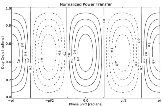
Normalized Power Transfer
-pi -pi/2 0.0 pi/2
Phase Shift [radians]
Figure 2.3: Power transfer relationship for voltage phase-shift (0), and pulse width
(6).
To visualize the power transfer of (2
),
Fig.
illustrates the normalized power transfer
for the phase space of
{0,
6}
E
[-7r,
7r], given V
>
0. The result is symmetric along both
O
= 0 and
6
= 7r, providing multiple solutions for a given power transfer, if the set is not
constrained further.
To address the continuum of parameter combinations, two specific switch modulation
cases are considered: phase-shift modulation, and pulse-width modulation. The basis for
the phase-shift modulation is to maintain a fixed pulse width, 6, and shift the phase of the
switching function,
0,
relative to the resonant current. Alternatively, in the pulse-width
modulation (PWM) method, the pulse width, 6, is controlled such that the high side switch
remains on for the duration required to obtain the required energy transfer at a chosen
0.
In both cases, the turn-on and turn-off transitions for all devices can be selected such
that they occur under zero-voltage conditions. The selection process is explored further in
-Section
2.5.
The primary side full-bridge inverter is controlled by phase-shifting the two halves of
the canonical switching modules in opposing directions relative to a reference, with each
operating at a fixed one-half duty cycle. This phase shift is what controls the pulse width,
seen at the output as a differential waveform. The average power transfer over a switching
cycle can be found, using the same method in
(2.3),
to be
VtIr
Pr = 2
r sin(6/4) cos(O),
(2.7)
7
where 6 denotes the pulse width, and the phase 0 denotes the difference in phase between
the output voltage waveform and the series resonant current, expressed in (switching cycle)
radians.
2.2.2
Equivalent Impedance
The input impedance of the canonical switching module, as shown in Fig.
2.
1,
is important
in the design of the converter, particularly the full-bridge inverter and transformation stage.
The combination of the buffer-block and cycloconverter act as an effective load during the
converter operation, and understanding how this load changes over time, or through changes
in the control parameters, can significantly influence the implementation.
With the resonant current waveform ir(t) defined as a sinusoid in
(2.
1), the fundamental
component of vr (t) can be used to calculate the effective input impedance of the switching
block at the operating frequency
ww.
Using phasors, ir(t) and
Vr(t)
can be written (with
the
ej'swt
factor omitted) as
2.2
System Modeling
Figure 2.4: The input impedance notation of the canonical switching module.
I =
r =Ir
2
(2.8)
(2.9)
The impedance driven by the current source, as shown in Fig. 2,1, is written simply as
Zr -Ir
Vt 2
j
Zr
=-
sin(6/2)ei
0.
Ir 7
(2.10)
(2.11)
This result indicates that the canonical switching module can present a variable
magni-tude complex load based on the selection of control variables 6 and
0.
Use of the current and voltage phasors in (2.
)
and
(2.1)
can also be used to calculate
Pr
=
1Re {IrVt - sin(6/2)eio
(2.12)
P= Vtrsin(3/2)Re
2
r
{eJO}
(2.13)
VtI
Pr =
7rrsin(6/2) cos(O),
(2.14)
which matches the result found in (2,6').
2.2.3
Time-Dependent Analysis
The calculation of the time-averaged power transfer and effective load impedances in are
useful for understanding the steady-state operation and driving requirements for the
canon-ical module. However, the operation over time scales much longer than the switching period
are also of interest, particularly when a sinusoidal (e.g. grid) voltage is present, or when
power transfer requirements vary.
Provided that the rate at which the control variables and circuit parameters change allows
them to be considered constant over the switching cycle, then the solution for the
time-averaged power in (2. 14) can directly augmented to make the expression time dependent
P(t) = VttIr(t) sin(6(t)/2) cos(O(t)).
(2.15)
7F~
This same time dependence can be associated with other derivations, such as modeling
the time dependent input impedance as
2.2
System Modeling
V(t) 2
Z (t)
= -sin(S(t)/2)et.
(2.16)
This simple extension to create dependent relationships is due to the use of
time-averaged quantities over a switching cycle, eliminating the need for the switching details
similar to time-dependent (dynamic) phasor methods
[
].
One specific case of interest for the time-varying parameters is when a sinusoidal voltage
source is present and a proportional current is desired, as is the case for single-phase power
generation. This situation can be described by
Vt(t) = Vt sin(wit)
(2.17)
It (t) = It sin(woit)
(2.18)
Pt(t) = Vsin(wit)Itsin(wit),
(2.19)
where w is the angular frequency of the waveforms (e.g., the line voltage angular frequency,
such as 27r60 Hz). If the above desired terminal power transfer Pt(t) is equated to
time-averaged result in (2.),
V sin (wijt) It sin (wijt) = Vtsn(~ )-,()sin(6(t)/2) cos(6(t))
(2.20)
It
sin(wit) =
sin(S(t)/2)
cos(O(t))
(2.21)
an equivalency stating that the terminal current in
(2
)
can be defined as a function of
39-the resonant current, Ir(t), and -the switching function parameters, 6(t) and 6(t). From
this relationship, it is clear that there exists a minimum resonant current for which the
expression remains true, and is at its lowest when the switching function pulse width is half
of the period (6
=
r) and in phase with the resonant current (0
=
0)
irIt