Developing Highly Accelerated Life Test (HALT) Method to Improve Product
Robustness and Shorten Development Cycle
by
Chun-Ming Chang
Bachelor of Science in Materials Science and Engineering National Tsing Hua University, 2015
Submitted to the Department of Mechanical Engineering in partial fulfillment of the requirements for the degree of Master of Engineering in Advanced Manufacturing and Design
at the
MASSACHUSETTS INSTITUTE OF TECHNOLGOY September 2016
© 2016 Chun-Ming Chang. All rights reserved.
The author hereby grants to MIT permission to reproduce and to distribute publicly paper and electronic copies of this thesis document in whole or in part in any medium now known or hereafter created.
Signature of Author: _____________________________________________________________ Department of Mechanical Engineering August 05, 2016 Certified by: ___________________________________________________________________ David E. Hardt Ralph E. and Eloise F. Cross Professor of Mechanical Engineering Thesis Advisor Accepted by: ___________________________________________________________________ Rohan Abeyaratne Quentin Berg Professor of Mechanics &
Developing Highly Accelerated Life Test (HALT) Method to Improve Product
Robustness and Shorten Development Cycle
By
Chun-Ming Chang
Submitted to the Department of Mechanical Engineering On 15th August, 2016 in partial fulfillment of the requirements for The Degree of Master of Engineering in Advanced Manufacturing and Design
Abstract
Highly Accelerated Life Testing (HALT) is often used to identify the latent defects for the printed circuit boards (PCBs) during the early stage of the product development process. The inconsistency in executing HALT may not reveal the maximum amount of design weaknesses or intermittent failures, which would eventually lead to the premature product failure in the field and incur additional warranty expenses. The scope of this project has focused on establishing the standardized operating procedure (SOP) for Highly Accelerated Life Testing (HALT) using the DMAIC methodology for the electronic components such as printed circuit boards (PCBs) to help identify these latent issues in advance and increase product robustness. In addition to applying statistical tools to optimize several key process parameters such as soaking time and ramp rate, the related failure analysis and corrective actions were also demonstrated in this thesis. In summary, three major results are shown: first, following the DMAIC guideline, the standard operating procedure (SOP) of HALT was established and applicable to all types of printed circuit boards. Secondly, it was shown that the top three failure modes identified in HALT were almost identical to that of the field returns’. Last but not least, the relationship between the operating margins and the warranty replacement rate was also established. Although more data points are required to further consolidate the model, the current result has indicated that there is a declining trend of the warranty replacement rate for every increment of the temperature operating margins. Such mathematical relationship was then used in the economic model to justify the business benefit of HALT.
Thesis Supervisor: Dr. David E. Hardt Title: Professor of Mechanical Engineering
Acknowledgements
I would like to take this opportunity to express my gratitude to the people who have been very supportive throughout my education and time at MIT. First of all, deepest thanks to my parents, Chang-Ju, Fu-Mei and my sister Fang-Yu. Without your continuous encouragement and love, I would not have been able to accomplish so many wonderful things and tasks.
I would also like to express my sincere appreciation to my thesis advisor, Professor David Hardt, who has provided numerous insightful suggestions throughout the entire thesis project, made the Master of Engineering in Advanced Manufacturing and Design program possible and given me the chance to thrive in this competitive environment and advance together with lots of excellent counterparts from around the world. Thanks to Jose Pacheco for teaching me several important social skills and always being a great help throughout the program.
Special thanks to Jim McPherson, Jared Ouillette, Gabriel Kelly and Gregory Puszko, for giving me the opportunity to join Waters Corporation and providing me with the strong guidance throughout the project. A thousand thanks to Robert Dumas, Ian Klobucher, Brian Boucher, Jim Kehoe, Gary Bertone, Paul, Tony, Frank, and all of the professionals from Waters for your generosity, enlightenment, and efforts in helping me and my teammates with the necessary resources and assistance to overcome hurdles and reach our goals. The fruitful experiences at Waters were unmeasurable and I will not hesitate to work with all of you again to accomplish the next excellent project.
Last but not least, thanks to my teammates, Abhishek and Dexter, and all of my friends for your continuous support and caring along the way. I am really looking forward to continuing my journey with all of you together in the days to come.
Table of Contents
Chapter 1 - Introduction ... 10
1.1 Objective ... 10
1.2 Motivation ... 11
1.3 Problem Statement ... 12
Chapter 2 - Background Information ... 13
2.1 Waters Corporation Overview ... 13
2.2 Current Printed Circuit Board Development Process ... 13
2.3 Printed Circuit Board (PCBs) Field Failure Data ... 14
2.4 Introduction to Alliance e2695 Separations Module ... 15
2.4.1 Solvent Management System Overview ... 16
2.5 Introduction to ACQUITY UPLC Binary Solvent Manager ... 19
Chapter 3 - Theoretical Review ... 21
3.1 Background of Highly Accelerated Life Test (HALT) ... 21
3.2 Benefits of HALT ... 23
3.3 Temperature Homogeneity Test ... 24
3.3.1 Analysis of Variance (ANOVA) ... 24
3.3.2 Transient Heat Conduction in Semi-Infinite Solid ... 25
3.4 HALT Process and Profiles ... 26
3.4.1 Cold Step Stress ... 28
3.4.2 Hot Step Stress ... 28
3.4.3 Thermal Cycling ... 29
3.4.4 Vibration ... 29
3.4.5 Combined Vibration and Temperature Cycle ... 30
3.5 Failure Analysis and Corrective Actions ... 31
3.5.1 Intermittent Failures ... 32
3.5.2 Operating Limit of Electronics ... 32
Chapter 4 - Experimental Result and Analysis ... 34
4.1 Overview ... 34
4.3 Data Acquisition and Equipment Used ... 35
4.3.1 Temperature Measurement ... 35
4.3.2 Electronic Signal Measurement ... 35
4.3.3 Vibration Response Measurement ... 36
4.4 Experimental Step and Results ... 36
4.4.1 Test Boards ... 37
4.4.2 System Block Setup ... 37
4.4.3 Temperature Homogeneity Step ... 40
4.4.4 Cold Step Stress ... 49
4.4.5 Hot Step Stress ... 54
4.4.6 Thermal Cycling ... 62
4.4.7 Vibration ... 65
4.4.8 Combined Thermal and Vibration Cycle ... 67
4.4.9 Experiment Conclusion ... 69
Chapter 5 - Conclusion and Benefits ... 71
5.1 Establishment of the Standard Operating Procedure (SOP) for HALT ... 71
5.2 Correlating HALT Failures to Field Failures ... 76
5.3 Correlating Operating Margins to Warranty Replacement Rate ... 77
5.4 Economic Benefit ... 78
Chapter 6 - Future Work and Recommendations ... 79
List of Figures
Figure 2-1 - Alliance e2695 Separation Module [5]. ... 15
Figure 2-2 - Functionality of the Alliance plunger drive board ... 18
Figure 2-3 - An overview of the ACQUITY UPLC instrument ... 20
Figure 3-1 - Life cycle of the electronic components. Modified from O’Connor [6] ... 22
Figure 3-2 - Bathtub curve with and without HALT. Modified from McLean [7] ... 23
Figure 3-3 - Cross-over effect of HALT. Modified from Barnard [8]. ... 30
Figure 3-4 - The common-seen failure modes identified in HALT [9] ... 31
Figure 3-5 - Electronics under extremely low and high temperature ... 33
Figure 4-1 - The monitoring equipment used during HALT ... 36
Figure 4-2 - Overview of the PCBs ... 38
Figure 4-3 - Isolating the Alliance 425 board from the instrument ... 39
Figure 4-4 - Overview of the experiment setup ... 41
Figure 4-5 - Residual analysis for the thermal couple on the top and bottom, respectively. ... 44
Figure 4-6 - Interval plot of ANOVA for the temperature homogeneity test ... 45
Figure 4-7 - The thickness of Alliance Plunger Drive Board. The measurement is in inches. ... 48
Figure 4-8 - The cold step stress profile for (a) Alliance 425 (b) ACQUITY 422 ... 50
Figure 4-9 - The experiment for the cold step stress in Alliance board 425. ... 52
Figure 4-10 - The result for the cold step stress in ACQUITY 422 ... 53
Figure 4-11 - The hot step stress profile for Alliance 425 and ACQUITY 422 board. ... 55
Figure 4-12 - Root-cause analysis and corrective actions for Alliance 425 ... 58
Figure 4-13 - Monitoring the functionality of ACQUITY 422. ... 60
Figure 4-14 - Mitigating the temporary failures of ACQUITY 422. ... 61
Figure 4-15 - The thermal cycling profile for Alliance 425 and ACQUITY 422. ... 63
Figure 4-16 - The pressure profile of ACQUITY 422 board during thermal cycling ... 64
Figure 4-17 - Vibration profile of Alliance 425 and ACQUITY 422, respectively ... 66
Figure 4-18 - Combined cycle profile for Alliance 425 ... 67
Figure 4-19 - After the combined cycle, the capacitor was detached from the PCB ... 68
Figure 5-1 - Implementation of HALT under DMAIC guideline. ... 71
Figure 5-2 - Preliminary Preparation of HALT ... 74
Figure 5-4 - Field Failure Modes of ACQUITY 422. ... 76 Figure 5-5 - Warranty replacement rate (product robustness) v.s. operating margin ... 77
List of Tables
Table 4-1 - Raw data of the thermal couple Top-2. ... 46
Table 4-2 - ANOVA result for the thermal couple Top-2 and Bot-2 ... 46
Table 4-3 - FMEA of Alliance 425 based on HALT result ... 69
Chapter 1 - Introduction
1.1 Objective
The primary objective of this project is to construct a standard operating procedure (SOP) for the Highly Accelerated Life Test (HALT) and justify its economic benefits. The deliverables can be further categorized into three different perspectives:
(1) Overall Process Flow, Failure Analysis and Corrective Actions
Design a HALT program and its standard operational procedure (SOP) that is applicable to a variety of printed circuit boards (PCBs). This includes using statistical tools such as analysis of variance (ANOVA) and knowledge of heat-transfer to optimize certain key process parameters such as the chamber soaking time, ramp rate, and air duct positions. The operating limit (OL) of the PCBs are determined during each thermal or vibrational step stress profile and the related failure analysis as well as the mitigation actions to be conducted to alleviate the as-observed design weaknesses. The failure modes identified throughout the process are documented and compared with the field failure data to justify the purpose and economic benefits of HALT.
(2) Data Interpretation and Economic Analysis
Establish the relationship between product robustness (field return rate) and the operating margins identified in HALT. Based on such result, build a cost-tradeoff model to justify the economic benefit of the design change by taking unit production cost, overhead, consumable costs, and the increased/decreased failure rates and its effect on cost of quality into account.
(3) Fixture Design with High Vibrational Energy Transmissibility
to determine the right set up location for the testing. A proposed fixture module will be suggested as a foundation for HALT testing for the printed circuit boards used at Waters.
This thesis has focused on developing the overall process flow and the standardized procedure for HALT that will be applicable to different types of printed circuit boards (PCBs), with more emphasis on the temperature stress. The major content of this thesis will include the experimental setup, key process parameters optimization, and the related failure analysis, corrective actions, data interpretation and economic analysis. More detailed information regarding the experimental setup, process flow, and analysis of the vibration stress used in HALT can be found at Singh [1]. On the other hand, the standard operating procedure (SOP) for the HALT fixture design for PCBs, as well as the variation minimization of the fixture placement and the data acquisition process can be found at Chew [2].
1.2 Motivation
Waters Corporation is the leading analytical instrument manufacturer of high performance liquid chromatography (HPLC) systems and mass spectroscopy. In addition to the intricate mechanical components such as columns, pumps, syringes, and valves in the system, the electronic components such as the power supply and printed circuit boards (PCBs) that control all of the hardware also play critical roles in the instrument. It has been reported that due to the premature failure of the electronic components, the company has suffered from some profitability loss from warranty expenses and the related lower level of customer satisfaction. Although efforts and design verification has been made and conducted in reliability engineering during the design process and test engineering during the post-production stage, the unpredictability in shipment and end-user environment will still incur some additional stresses that will eventually lead to the pre-mature failure of PCBs. It is believed that the establishment of a standardized highly accelerated life test (HALT) process can not only help identify these latent defects in the early stage of product development process to save warranty cost, but also facilitate the communication between the reliability engineering, R&D engineering, and testing engineering department to design robust products within a relatively shorter period of time. The eventual goal of this project is to establish a standard operating procedure (SOP) for HALT and justify the economic benefits and trade-off
to implement such techniques.
1.3 Problem Statement
While design verification and instrument evaluation is embedded in Waters’ product development process, and reliability testing as well as post-production examination techniques such as in-circuit testing (ICT) or functional testing (FCT) are applied through the entire lifespan of the products before shipment to the customers, premature failures still occur in the field and have incurred some additional and unexpected warranty expenses. Although highly accelerated life test (HALT) process has been implemented for years within the corporation with an aim to identify the potential latent defects in the reliability engineering department, the absence of a standardized operating procedure (SOP) has made it difficult to compare and verify the results performed by different engineers and among different PCBs. A thorough investigation on figuring out the relationship between several key process parameters such as chamber soaking time, ramp rate, air duct positions, and the related failure analysis and corrective actions will be very valuable in terms of executing HALT. On the same note, possible issues may arise when discussing to what extent these components should be tested. There is often a trade-off between the production costs, testing costs, and cost of quality. For example, a new component can be introduced that meets the required functional specifications, and has a lower manufacturing cost, but if the failure rates of the component are higher compared to the old part, it may lead to a high service costs that outweighs the production cost savings. On the other hand, a component can be re-designed using the latest manufacturing techniques in order to improve quality and practically guarantee zero failures over the life of the component, but at a grossly increased production cost. There is a need to find the balance between production costs and the corrective actions costs when it comes to design or production changes. A successful HALT program will facilitate efficient screening of these scenarios and provide data to augment design process.
Chapter 2 - Background Information
2.1 Waters Corporation Overview
Waters Corporation is the leading analytical instrument manufacturer based in Milford, Massachusetts, that primarily designs, manufactures, and sells various kinds of liquid chromatography and mass spectrometry instruments. The majority of the company's customers are from life science, food science, environmental industries as well as academic and governmental sectors where researchers will need to use these analytical instrument in the drug discovery and development, genomics, proteomics and biopharmaceuticals research, as well as nutritional safety and quality control. In addition to instruments themselves, a large portion of Water’s business also includes the sale of chromatography columns, consumable products and comprehensive post-warranty service plans [3].
2.2 Current Printed Circuit Board Development Process
After the product management team has identified the business case and market requirement, design and development plan will be planned and initiated. The product development team usually consists of systems engineering, mechanical engineering, electrical engineering, software engineering, and compliance engineering. The specified performance of the alpha, beta, and pre-production (PP) prototype of electronic boards are verified within the R&D setting. On the other hand, the long-term stability as well as the life testing are carried out in the reliability engineering department. Although depending on the functionalities of different instruments, the reliability testing will usually include the leak test and burn-in test to check whether the PCBs are still able to perform their intended functions under extreme operating conditions. Once all of the necessary validations are satisfied, the electronic boards are sent to mass-production. Post-production units are examined in the testing engineering department by using in-circuit testing (ICT) or functional testing (FCT) unit. In most cases, printed circuit boards (PCBs) are identified as good units and will meet the specifications. On the other hand, the defective ones are usually identified, fixed or removed when tested under ICT or FCT, and therefore do not result in eventual equipment failures.
However, some of the latent defects of the PCBs might not be detected throughout the current design verification process despite the aforementioned efforts. This is why HALT process was implemented with an aim to reveal these potential failure modes to prevent premature failures from happening in the field.
2.3 Printed Circuit Board (PCBs) Field Failure Data
Due to the large amount of products within the corporation and the limited time frame of this project, an economic analysis was performed before proceeding to experiments to narrow down the printed circuit boards (PCBs) to one or two instruments. For example, although some of the desired candidates have higher failure rate, the fixtures for in-circuit testing (ICT) or functional testing (FCT) are not in place, which will result in a rather challenging scenario for HALT engineers when it comes to failure and root-cause analysis. The trade-off between different choices given the available resources, overhead and economic impact to the company were therefore evaluated and discussed in advance. The focus was narrowed down to two specific motor driving boards used in two different solvent management systems. The first of them is the plunger drive board used in the Alliance e2695 Separation Module instrument. Because of the continuing efforts in design modification and corrective actions, the board is now very robust, with a warranty replacement rate of only about 0.1%. So, its experimental results will therefore serve as the standard of robustness. The second is the personality PCB used in the ACQUITY UPLC equipment’s Binary Solvent Manager (BSM). The warranty replacement rate of the BSM personality PCB has an average of 8% throughout the years. Experiments will be conducted on these two boards, respectively, to compare the operating margins between the two. Afterwards, the relationship between the operating margins and the field warranty replacement rate can be established.
2.4 Introduction to Alliance e2695 Separations Module
Since the Alliance plunger drive board was selected to be the benchmark of the entire project, the related functionalities of the electronic board must be well understood before proceeding to the experiments. A large content of this section was based on “Waters Alliance e2695 Separations
Module Operator’s Guide” [4]. The Alliance e2695 Separations Module is a high performance
liquid chromatography (HPLC) instrument that integrates and combines the solvent and sample managers in a single unit and is capable of performing all of the major separations functions. On the other hand, it also has the capability to mix four different solvents at once. The overview of the unit is shown in Fig. 2-1.
2.4.1 Solvent Management System Overview
Since the plunger drive board only controls the mechanical components of the solvent manager, the focus has been narrowed down to the solvent management system in the Alliance unit. The main purpose of the solvent management system is to blend and deliver solvents from the reservoir bottles to the sample management system. The process flow starts from blending solvents via the gradient proportioning valve (gpv), and then the mixed flow goes through the inlet check valve and into the primary piston chamber while the accumulator piston delivers solvent to the next pressure transducer. Before the accumulator chamber becomes empty, the solvent in the primary piston chamber is pre-compressed to a lower pressure so the solvent can be delivered from the primary to the accumulator piston chamber under pressure. By having such pre-compression mechanism, constant pressure and flow rate can be maintained throughout the process. Afterwards, the solvent flows through prime/vent valve and into an in-line filter where the solvent flows to the sample management system. The flow path is shown in Fig. 2-2 (b).
The chosen plunger drive PCB is used to communicate with the CPU board as well as control various mechanical components in the solvent management system. The overall functionality of the plunger drive PCB is shown in Fig. 2-2 (a). Throughout the HALT process, four major functionalities will be monitored continuously via hyper-terminal on the computer: the primary/accumulator pump motors, the seal wash, the gradient proportioning valve (GPV) and the fan. Each of the mechanical component’s functionality is explained in more detail below.
2.4.1.1 Primary/Accumulator pump motors
The purpose of the primary/accumulator pump motors is to drive the plunger and deliver the solvents continuously into the sample manager. The primary and accumulator step motors are functionally identical and have alternating movement that is driven by inverting of sine and cosine wave by a micro-step drive to take in and deliver out the solvent smoothly throughout the operation. To be identified as functioning properly, the system will have to maintain a constant flow rate and pressure throughout the process. Having the encoders as well as the RS232 serial communication
the process by sending command to the CPU and plunger drive board via the hyper-terminal software.
2.4.1.2 Seal Wash
The seal-wash functions to extend seal life by using the solvent to lubricate the plunger and wash away any residual solvent or contamination passing through the plunger seal of each piston chamber. The seal wash solvent flows from a reservoir to the solenoid wash pump and then flows from the primary head into the cavity behind the plunger seal, in the accumulator head. The washed solvent eventually flows to waste. Whenever the solvent management system is delivering solvent, the plunger seal wash pump intermittently circulates the wash solvent. The functionality of the seal wash can be checked continuously throughout the HALT process by listening to the clicking sound of the solenoid activated by the hyper-terminal command.
2.4.1.3 Gradient Proportioning Valve (GPV)
The solvent blending function is mainly performed by the gradient proportioning valve (GPV), which has the capability to mix four different solvents in different proportions at once. Predictable gradient segments regardless of solvent compressibility and system backpressure can be produced. Solvent selection and proportioning take place on the low-pressure side of the solvent delivery system. The solvents will then continue to blend in each of the piston chambers. As before, the functionality of GPV could be checked continuously throughout the process by checking whether users can activate it via the serial communication.
2.4.1.4 Fan
The main purpose of the fan is to provide overall cooling for the plunger driver board to prevent it from overheating. A tachometer is embedded in the fan’s electronic circuit to monitor the performance of the fan by detecting whether it is able to provide air flow or is operating at least above 63% of its normal speed.
Figure 2-2 - Functionality of the Alliance plunger drive board. (a) An overview. (b) Solvent flow throughout the system.
P LUNGER D RIV E PCB (W AT270919) 715004566 R EV . A C OMPANY C ONFIDENTIAL - P ROPRIETARY I NFORMATION - F OR I NTERNAL U SE O NLY 3 OF 8 Interconnection diagram
Figure 3 - Plunger drive PCB interconnections
Plunger Driver PCB WAT270919
J1 J5 J3 J6 J7 J2 J4
Primary/Accumulator
pump motors Seal wash GPV
Power Supply WAT270926 WAT270927 Fan WAT270909 WAT270923 700001031 Alliance CPU PCB
WAT270915 eAlliance CPU PCB700004462
Sparge valve assy Not used
(a)
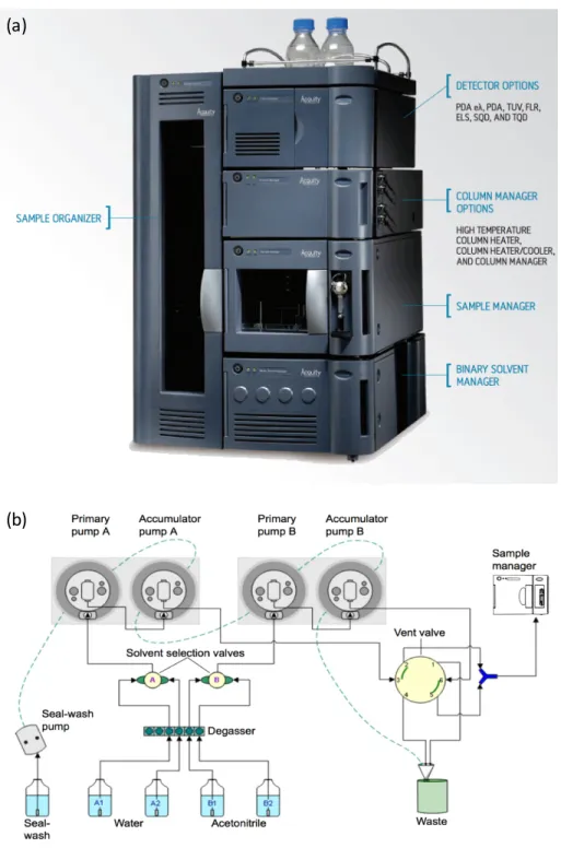
2.5 Introduction to ACQUITY UPLC Binary Solvent Manager
The second board chosen for this project is the personality PCB used in the binary solvent manager (BSM) in the ACQUITY UPLC system. A large content of this section is based on “Waters’
ACQUITY UPLC System Operator’s Guide” [5]. Each of the solvent managers has two
independent pump systems, A and B, which contain two linear-drive actuators in total. The two pump systems combine their two solvents at a filter/tee mixer. From there, the solvent mixture will flow to the sample manager. The solvents’ relative mixing ratio is controlled by the chromatography software by varying the flow rate of pump A relative to pump B. A pressure transducer in each pump head relays pressure data to the solvent manager, whose firmware measures pump head pressures during the pumping cycle. The solvents in both the A and B portions are pre-compressed independently to ensure consistent solvent delivery and minimize the pump-induced detector baseline disturbances. In conclusion, the personality PCB controls the following function: the fluid flow inside the instrument, the communication with the CPU board, the connection to external devices and mechanical components such as pump motors, vent valves, SSV valves, fan…etc., and the connection with power supply. An overview of the instrument and process flow is shown in Fig. 2-3 (a) & (b). Due to the inherent complexity of the system, the main focus will be put on monitoring its capability to maintain a constant flow rate and system pressure throughout the HALT process. This functionality testing can be done by using the company’s Empower software that is designed for the customers.
In sum, the functionality of the Alliance plunger drive board will be monitored continuously by activating and sending commands via the hyper-terminal software to check the status of the pump motors, gradient proportional valves (gpv), seal wash and fan. On the other hand, the functionality of the ACQUITY UPLC BSM’s personality board will be checked by using the company’s built-in Empower software to monitor the system’s pressure as well as any error message that might surface up throughout the entire HALT process. Should any of the error messages show up on the screen in either cases, it will be an indication that the control logic behind certain mechanical components has failed and will require further failure analysis and mitigation actions.
Figure 2-3 - An overview of the ACQUITY UPLC instrument. (a) Different modules used in UPLC. (b) Functionality of the binary solvent manager (BSM) personality board.
(a)
Chapter 3 - Theoretical Review
The background, potential economic benefits, and process of HALT will be elaborated in this chapter. Secondly, the statistical tools such as analysis of variance (ANOVA) and the heat transfer knowledge applied during the temperature homogeneity test are also depicted. Last but not least, the physics behind the operating limit of electronics as well as the cause of the well-known intermittent failures identified in HALT are also explained.
3.1 Background of Highly Accelerated Life Test (HALT)
The unpredictability in the end-user environment such as the temperature change caused by air-conditioning problems, unexpected vibration resulted from occasional collisions as well as the variability in shipment quality from manufacturers to customers will all lead to the potential product premature failures. Unlike most non-electronic equipment, electronic components’ reliability is often difficult to test since most of the time they are encapsulated after production. Most of the time, the defective units will be identified, fixed or removed when tested during burn-in test, burn-in-circuit test (ICT) or functional testburn-ing (FCT) after production, which therefore do not result in the unexpected field failures. However, the culprit behind the premature failures of the printed circuit boards (PCBs) are called “freaks”. Examples of these issues include weak soldering, silicon, oxide and conductor imperfections, impurities, and non-hermetic packages. Identification of these freaks might not be likely during the initial reliability or functional testing in the facility but they will eventually lead to the field failures due to the aforementioned uncertainties in end-user environment [6] [7]. This is shown in Fig. 3-1; most of the failures are infant mortalities and can be identified and eliminated before shipment to customers. However, freak failures will usually not reveal themselves until the later stage of products’ life span and eventually result in the increase of warranty, service and overhead cost.
HALT is conducted to stimulate the latent defects and replicate as many field failure modes as possible to locate the design weaknesses in the early stage of product design and development process so as to improve overall robustness of the product. Unlike traditional environmental stress
screening (ESS), HALT utilizes a series of thermal steps, vibrational steps, and product specific stresses to expose the intermittent failures or latent defects within a shorter period of time. After HALT process, the potential failures can be fixed in advance and the product will become more robust in the field. Therefore, not only the field failure rate will be reduced significantly but also the testing and service costs can be saved accordingly. The eventual goal of HALT is to increase the overall customer satisfaction, reduce service and warranty replacement cost.
Figure 3-1 - Life cycle of the electronic components. Modified from O’Connor [6].
©2016 Waters Corporation
F
ai
lu
re
R
at
e
Time
Failure RateF
ai
l
u
r
e
R
at
e
Time
Failure Rate
Freak Population Infant Mortality3.2 Benefits of HALT
The benefits of HALT include the increased product reliability after production and indirect cost savings by freeing up resources and competitive advantages. First of all, because of the relatively short testing time required for executing HALT, it will barely add burdens to the original design verification schedule. Secondly, due to increased robustness of the product after HALT, R&D engineers can focus more on developing next generation products instead of executing rework and re-design adjustments along the lifespan of the released products. Lastly, the decrease in the premature failures and quality variations will definitely lead to a higher level of customer satisfaction, lower overhead, as well as less service and warranty cost. Although some additional cost might be incurred by HALT during the original product development process, the savings in the long-term will result in the higher profit for the company throughout the product lifespan. The elimination of the failure rate aberrations and the extended lifespan of the product after implementing HALT are shown in Fig. 3-2. The lower, and more flat level of the mid-section of the bathtub curve indicates that the product robustness is increased.
Figure 3-2 - Bathtub curve with and without HALT. Modified from McLean [7]. ©2016 Waters Corporation F ai lu re R at e Time Failure Rate
F
ai
l
u
r
e
R
at
e
Time
Failure Rate
Without HALT With HALT3.3 Temperature Homogeneity Test
During the HALT temperature step stress, several key process parameters such as ramp rate, soaking time, and air duct positions should be taken into consideration in order to make the PCBs reach thermal equilibrium as soon as possible to minimize the testing time. In terms of the determination of soaking time, it is usually based on experiences or purely by board surface temperature measurement, and lack of a systematical approach for optimization. As a matter of fact, several different sources have reported different soaking time needed. This ranges from 10 to 30 minutes, depending on the products’ thermal mass and the required test diagnostics time [8].
A temperature homogeneity test should therefore be conducted in the beginning of HALT to confirm what is the optimal soaking time for the specific types of products to reach thermal equilibrium based on the current fixture setup and air duct positions. To facilitate the thermal-energy transfer, a sufficient number of air ducts should be used to ensure maximum board area coverage. In a series of experiments, actual PCBs temperature was measured by several thermal couples across the boards and compared with the chamber set-point. Analysis of variance (ANOVA) was performed to verify whether there was a difference in terms of the surface temperature response under different soaking time for each location on the printed circuit boards (PCBs). Due to the inherent nature of the multiple layers of PCBs, heat transfer through the layers of the board was also investigated to ensure that the center layer will also have the same or similar temperature as that at the surface by the end of each temperature soaking step.
3.3.1 Analysis of Variance (ANOVA)
Many of the sources [7] [9] have indicated that 10 minutes is the desired the soaking time for thermal stabilization. However, no one has been able to prove this in a statistical way. Analysis of Variance (ANOVA) is an effective statistical tool to test the equality of mean values for various factors. Its theory is based on comparing the variation within and between different groups of sample. The final output will be the interpretation as whether there is a significant difference between the mean value of different groups of sample. The detailed theory and calculation can be
be valid, the assumption that model errors or observations are normally and independently distributed with the same variance in each factor level should be checked in advance. The normality assumption can be checked by constructing a normal probability plot of the residuals, which are the difference between each observation and the factor-level mean value. Secondly, the independence assumption can be checked by plotting the residuals against the experiment run order. The observations should be independent of the sequence of run orders. Lastly, the equal variances assumption can be checked by plotting the residuals against the factor-level mean value. The variability or spread in the residuals should be randomly distributed and not dependent on any specific value [11].
3.3.2 Transient Heat Conduction in Semi-Infinite Solid
Since the thickness of the PCBs is small compared to the width and length, it can be modeled as a semi-infinite solid and transient heat conduction can be applied to calculate its temperature response at a specific location within a specified time. In a one-dimensional semi-infinite solid heat conduction problem, the temperature at a specific location and time can be described as 𝑇 𝑥, 𝑡 , with x being the location and t representing the time. If the initial temperature of the board is 𝑇%, and there is a constant surface temperature 𝑇 0, 𝑡 = 𝑇), then the temperature 𝑇 𝑥, 𝑡 can be calculated from the following formula [12]:
* +,, -*.
*/-*. = erf
+
3 4, , 𝑤𝑖𝑡ℎ α being the thermal diffusivity and equal to 8 9: .
• k is thermal conductivity (W/(m·K)) • ρ is density (kg/m³)
• Cp is specific heat capacity (J/(kg·K))
Since the PCBs consist of multiple layers with different content of copper wires in each one of them, the thermal conductivity can be further categorized into two categories: in-plane and through-plane thermal conductivity. The formula are given by as the following [13]:
In − plane 𝑘B(𝑊 𝑚 ∗ 𝐾) = 0.8 + 350 ∗ (𝑍OP/𝑍) Through − plane 𝑘W 𝑊 𝑚 ∗ 𝐾 = [1.69 1 – 𝑍]^
𝑍 + 0.026 𝑍]^
𝑍 ]-a
ZCu is the total thickness of continuous copper layers in the PCB with total thickness Z. Here the emphasis will be on the through-plane conductivity kn since the objective is to calculate how much time is required to reach thermal equilibrium from surface to the center layer. Due to the fact that the thickness of copper wire is found to be negligible relative to the total thickness of PCB; therefore, kn will have a value approximately equal to 0.6 Wm–1K–1. Since most of the PCB is made out of epoxy or “FR4” (flame retardant), the density and specific heat capacity will be calculated as the FR4’s. The density ρ is therefore 1850 kg/m3, heat capacity Cp is 0.6 kJ/(kg•K) [14] [15].
3.4 HALT Process and Profiles
Before proceeding to HALT profile, a thorough understanding of the failure modes of the device under test (DUT) is necessary. In reality, the majority of electronic hardware failures were not caused by component failures but instead by bad interconnects and connectors, excessive environmental stresses, and improper end-user handling. On the other hand, it has been reported that the defects uncovered in HALT stressing will almost overlap with that in the field. HALT has been shown to uncover the same types of flaws as that in the field within a relatively shorter period of time, possibly with a time reduction from months to only hours [16]. It is therefore important to discern the possible field failures from the service engineers beforehand. A detailed Pareto chart for ACQUITY 422 failures is discussed in Chapter 5.
In total, there will be five different steps in the HALT process: cold temperature step stress, hot temperature step stress, rapid thermal cycling, vibration step, and the combination of rapid thermal cycling and vibration. The reason for conducting the experiment step by step is to better facilitate the failure and root-cause analysis. Before proceeding to the discussion of the detailed profiles of each step, some of the key measurements need to be defined:
• Lower operating limit (LOL): The system or equipment has lost its intended functionality at this specific temperature during the cold temperature step stress, but when returning back to the previous stress level or room temperature, the system goes back to normal without the need of any further physical repair or component replacement. It usually occurs because there is an intermittent failure, or a so-called “soft failure”.
• Lower destructive limit (LDL): After identifying the LOL, and making sure that the failure modes behind LOL has been found and mitigated, the stress is then increased to the next level. When reaching certain temperature level, the system will show anomalies again but this time it will have to undergo some certain degrees of repair or component replacement in order to function properly again. This limit is abbreviated as LDL and also sometimes called “hard failure”.
• Upper Operating Limit (UOL): During the hot temperature stressing step, the system or equipment will output an anomaly or not be able to function properly at this certain temperature. But when returning to the room temperature or previous stress level, the system can recover by itself without any further repair. It usually occurs because of an intermittent failure, or a so-called “soft failure”.
• Upper Destruct Limit (UDL): After failure modes are identified and fixed for the UOL, the stress level is then increased to further above UOL using the same procedure. When UDL is reached, the system will not go back to normal if simply returned to the room temperature or previous stress level. Some degrees of repair or components replacement will be required. It is usually related to “hard failure”.
• Vibration Operating Limit (VOL): It is the vibration stress level where the product starts to malfunction or a specification can no longer be met, but the instrument will be able to return back to normal without any physical repair after such stress is decreased or removed.
• Vibration Destruct Limit (VDL): Similar to the concepts mentioned before, after the failure modes and corrective actions has been undertaken for the VOL, the vibration level can follow
the same procedure and go to the next higher level. When reaching the VDL, the product will no longer be able to operate even when going back to a lower level of stress unless some certain degrees of repair task is performed.
3.4.1 Cold Step Stress
The cold temperature step is usually the least detrimental one and therefore is performed first in HALT. In the beginning of the process, the chamber temperature set point is at room temperature. Afterwards, the temperature is decreased 10~20°C per thermal step and the product soaked at each specific temperature for around 10~15 minutes for thermal stabilization. The desired soaking time and ramp rate applied is based on the previous temperature homogeneity test. However, if the temperature overshooting problem is severe, a lower ramp rate can be used to counterbalance such discrepancy. The temperature continues decreasing until some irregularities or anomalies occur. After finding out the lower operating limit (LOL), failure analysis and mitigation actions should be performed before proceeding to the next level of stress. Only by doing so can the engineers distinguish the failure modes. The lower destructive limit (LDL) is determined whenever possible [7].
3.4.2 Hot Step Stress
The hot step basically follows the same procedure as the cold step stress. The ramp rate and soaking time is the same as that used in cold step stress. Upper operating limit (UOL) is encountered first and the relevant failure modes and corrective actions should be performed before reaching the next level of stress. The upper destructive limit (UDL) can be determined whenever possible. In conjunction with the previous cold step stress result, the product’s thermal operating range is therefore defined [7]. The thermal range identified from the cold step stress and hot step stress is important in that it will be applied to the following thermal cycling and combined cycle step.
3.4.3 Thermal Cycling
The main goal of this step is to detect whether there is a mismatch of the thermal expansion coefficients, PCB mounting problems, weak solder joints, and IC package integrity [17]. Usually it consists of five rapid thermal cycles, and the product will be tested after completion to check whether it is still functioning properly. During the cycling, the product is subject to maximum cooling and heating rate as much as possible between the adjusted thermal limits. The adjusted thermal limits applied in this case will be 10~20°C below UOL and 10~20°C higher than LOL, with UOL and LOL being determined in the previous cold and hot steps. At each temperature step, the product is also soaked about 10~15 minutes in order to reach thermal stabilization [7].
3.4.4 Vibration
Although many have argued that the product will never be exposed to the severe vibration condition in the field, due to the ‘crossover effect’, vibration might actually be able to induce the same failure mode as that caused by thermal cycling in the field [8], as shown in Fig. 3-3. It is therefore essential to include the vibration step as part of the HALT profile. During vibration, a three-axis vibration consisted of six degrees of freedom-style pneumatic system is used and a step stress profile is applied. The degree of vibration used in HALT is usually measured by an accelerometer and characterized by the term “Grms”. The Grms value of the signal is calculated by taking the average of each signal point’s squared magnitude, and then computing the square root of the average value again in the end [18]. According to industrial experiences, it was recommended to start the profile with 5 Grms initially, and use a step increment of 2~3 Grms throughout the process. During the entire profile, the chamber temperature should be maintained at 20~25°C. The dwell time of each vibrational step should be 10 minutes or as long as it is sufficient to perform diagnosis. The fixture might be designed for different types of PCBs with different geometries; however, it does not need to be the same as that used in product assembly or end-use application [7]. When the first anomaly is encountered, the vibration stress level is returned to the previous level to check whether the equipment will recover by itself. If it does, then a vibration operating limit (VOL) is found and failure analysis as well corrective actions must be performed before proceeding to the next level of stress.
Figure 3-3 - Cross-over effect of HALT. Modified from Barnard [8].
3.4.5 Combined Vibration and Temperature Cycle
In this step, the product is subject to the combination of the vibration and thermal cycling stress. The thermal profile will be the same as that used in the rapid thermal cycling. On the other hand, the vibration step will be equal to the vibrational destructive limit (VDL) determined before divided by five, and increased one step at a time throughout the five cycles of test. In sum, there will be five thermal cycles in conjunction with vibration and other environmental stresses such as power cycling, or humidity. During the thermal cycling, the vibration step stress was found to be important because the vibration response of many products changed as the temperature changed. Cross-over effect might take place and stimulate some additional failure modes that will otherwise go undetected [9]. ©2016 Waters Corporation
F
ai
lu
re
R
at
e
Stress
Failure RateF
ai
l
u
r
e
R
at
e
Time
Failure Rate
Cross-Over Effect HALT Field Vibration Temperature3.5 Failure Analysis and Corrective Actions
After identifying the operating limit or destructive limit in each of the aforementioned steps, failure analysis is conducted and the root-cause must be understood and fixed whenever possible in order to reach the next level of stress and reveal higher level of failures. If modifications cannot be made because the failure is not easily correctable, the sensitive areas are kept at a lower stress level than the rest of the product by, for example, using thermal barrier material and epoxy to reduce the temperature and vibration response, respectively.
In HALT, most of the failures can be fixed at low to no cost because they might simply be caused by incorrect components or inappropriate materials selections [9] [19]. Some of the common-seen failures identified in HALT was summarized by Silverman [9] through the study on 47 products from 33 different companies across 19 different industries. The investigation results were characterized as a Pareto chart as shown in Fig. 3-4. The majority of failure modes shown in here were common field failure modes observed in the field and HALT merely stimulated and accelerated the failures that will not take place until a much longer period of time.
Figure 3-4 - The common-seen failure modes identified in HALT [9].
0 20 40 60 80 100 0 20 40 60 80 100 P er ce nt age Q uan ti ty
Summary of failures found in HALT
Qty Cumulative Percentage
3.5.1 Intermittent Failures
One of the most well-known failures seen in HALT are the intermittent failures of electronics. Intermittent signals might be caused by solder joint fracture that periodically open and close. The potential stress behind such scene are vibration, thermal, and other environmental stresses such as power cycling or humidity. When such stresses caused fracture to open and close, the circuit of that solder ball will also unpredictably open and close from time to time, which then resulted in an intermittent signal. This kind of latent defect will usually be able to pass a bench-test such as ICT or FCT because damaged joints can still make temporary contact [20]. Since such intermittent failures would eventually evolve into permanent failures after some period of time, it is therefore very vital to identify the existent of such failures as early as possible to prevent them from happening in the field.
3.5.2 Operating Limit of Electronics
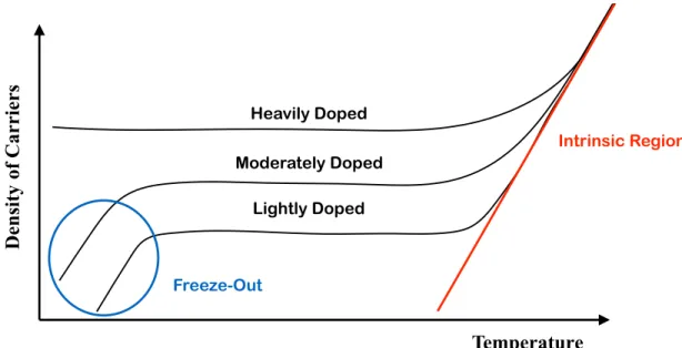
The main goal of HALT is to replicate or precipitate the field failures modes of the products within a shorter period of time. The other objective is to find out the real operating limit of the printed circuit boards (PCBs). It has been reported that the operating limit of several commercial office products actually had operating limits that are far beyond the manufacturer’s specification [9]. The physical and scientific reasoning behind such limits can be explained as the following [21]. Semiconductor devices operates based on having different amount of doping elements on the two sides of the junction in the substrate. A p-n junction is created with the major carrier (electrons or holes) moving faster in one direction than the opposite direction. Through different arrangement of n-type, p-type, and intrinsic regions within the device, different charge carriers speed across different regions could be obtained and yield different electrical properties. Each semiconductor device usually has its own and different temperature specifications, and is illustrated by low and high operating temperature limits. Such operating limits are determined by a number of factors and there is usually not a universal rule that is applicable to all devices such as: basic semiconductor material physical properties, different types of device (diode, bipolar transistor, field-effect transistor..., etc.), different device design (geometry, dimensions, analog or digital
According to research findings, the semiconductor in generally will continue to perform the normal characteristics within conventional limits ranging from −65°C to +125°C. Usually, the applicable temperature range corresponds roughly to the flat region of each curve, as shown in Fig. 3-5. Whenever the upper operating limit or lower operating limit is reached, the device will lose its intended functionality as a semiconductor.
The upper operating limit can usually be explained as the thermal ionization of the substrate materials. That is, as temperature increases, the sufficient thermal energy can ionize substrate atoms such as Si in addition to the dopant atoms, which can lead to the generation of excessive charge carriers in the conduction and valence bands that neutralize the carriers on both side of the junction and result in the formation of intrinsic region. The existence of such neutral zone will result in the loss of carrier mobility in the p-n junctions and therefore make the device lost its intended functionality. On the other hand, the lower operating limit is determined by the ionization energy of the dopants. If the temperature is too low, the dopants will not have sufficient thermal energy to be ionized and produce carriers. Therefore, insufficient carriers will be in the substrate, which will result in a condition called "freeze-out”, and cause the device to lose its intended functionality.
Figure 3-5 - Freeze-out and intrinsic behavior of electronics under extremely low and high temperature. Reproduced and modified from Kirschman [21].
©2016 Waters Corporation D en si ty of C ar ri er s Temperature
F
ai
l
u
r
e
R
at
e
Time
Failure Rate
Heavily Doped Moderately Doped Lightly Doped Freeze-Out Intrinsic RegionChapter 4 - Experimental Result and Analysis
4.1 Overview
The Alliance equipment’s plunger drive board in the solvent management system was selected to be the preliminary experimental subject because it has the lowest field return rate. The established standard operating procedure (SOP) used on Alliance plunger drive board as well as the obtained operating margins would be served as the benchmark of robustness. The latter part of the experiment would then be focused on the ACQUITY UPLC binary solvent manager (BSM)’s personality PCB to make comparison with the result of Alliance’s plunger drive board. In both of the cases, the operating margins and the identified failure modes would be compared with the field failure data to further prove the validity of the as-established SOP.
4.2 Functional Testing
The functionality of the tested subject was monitored continuously throughout the process to locate the maximum amount of design weaknesses. In the Alliance’s plunger drive board, there were four main functionalities being monitored throughout the process: gradient proportional valves (gpv), primary/accumulative motors, fans, and the seal wash. The diagnostics were run continuously through the entire HALT testing via the serial communication port (RS232) to the hyper-terminal software on the computer. The command was sent from computer continuously to the CPU board to activate the signal on plunger drive board. The frequency of sending such command would therefore be viewed as the product specific stress in this case. The operating limit (OL) of the board is determined once the hyper-terminal communication output the sign of “hardware failure” or revealed the sign of the inability to activate certain functionality.
In the case of ACQUITY’s personality PCB, the functionality was checked by using Waters’ Empower software. On such a platform, system’s and pump motor’s pressure can be monitored continuously throughout the testing. Should any of the abnormality appear, the software will be
applied to serve as the product specific stress during HALT testing. The operating limit (OL) of the board is determined once there is a pressure ripple or fluctuation at certain time interval that exceeded 0.1% of the system average pressure or whenever there is an error message showing up.
4.3 Data Acquisition and Equipment Used
In order to execute the HALT process accurately, the following equipment was used in different settings so as to measure and monitor the product response, and provide feedback to the process.
4.3.1 Temperature Measurement
In total, eight type K thermal-couples were used in conjunction with the Keysight 34972A LXI Data Acquisition / Data Logger Switch Unit [22]. The Keysight Data Acquisition Unit has built-in USB built-interfaces and the data can be easily uploaded to a laptop. It has the capability to measure 11 different input signals including temperature, voltage, current, wire resistance or frequency and period. These thermal-couples were used to measure the surface temperature of the PCBs with a time interval of every 5 seconds.
Inside the HALT chamber itself, there was a built-in thermal couple that measures the environmental temperature of the chamber. This thermal couple forms a feed-back loop with the chamber’s temperature control logic to maintain the chamber temperature in time, as shown in Fig. 4-1 (a). This temperature measurement is called the process temperature.
4.3.2 Electronic Signal Measurement
Oscilloscope was used to monitor the electronic signals in time via the testing points on PCBs. Such measurement was conducted throughout the process to facilitate the following failure analysis and corrective actions.
4.3.3 Vibration Response Measurement
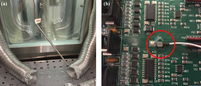
Accelerometer was used in conjunction with the LabVIEW program to measure the response of either the fixture or device under test (DUT). Wax or mechanical mounts were used to secure the accelerometer in place. The accelerometer is shown in Fig. 4-1 (b).
Figure 4-1 - The monitoring equipment used during HALT. (a) Process thermal couple (b) Accelerometer.
4.4 Experimental Step and Results
In the following sections, the experimental process was discussed and explained in detail. In the beginning, a system block diagram was constructed to discern the target of interest and isolate it from the rest of the instruments. Afterwards, the temperature homogeneity step was performed first to verify the required soaking time and ramp rate for the PCBs to reach thermal stabilization based on the current air duct positions and fixtures. In conjunction with the heat-transfer calculation, the optimal soaking time was obtained and used throughout the HALT process. Following the execution sequence of cold step stress, hot step stress, thermal cycling, vibration, and combined cycle of thermal cycling and vibration, the operating limit of each of the step stress was identified, and failure analysis as well as corrective actions were performed to mitigate such
4.4.1 Test Boards
As mentioned before, the printed circuit boards (PCBs) tested in this project were the Alliance plunger drive board (from now on abbreviated as Alliance 425) and ACQUITY UPLC BSM personality PCB (from now on abbreviated as ACQUITY 422), respectively, as shown in Fig. 4-2. Although the two boards were used in different instruments, both of them mainly controlled the major mechanical components in their sample manager system. The experimental data and operating margins can therefore be compared.
4.4.2 System Block Setup
It is very important to isolate the PCB from the rest of instrument to make sure that only the PCB is subject to temperature and vibration cycle or any other desirable product specific stresses. By doing so, engineers can benefit in the later stage of failure analysis and focus the root-cause analysis on the electronic components themselves. Extension cables connecting between the PCB and instrument should be made in this stage to make sure the PCB can be placed inside the HALT chamber and isolated from the rest of the other components successfully. The system block diagram and actual setup is shown in Fig. 4-3.
Figure 4-3 - Isolating the Alliance 425 board from the instrument. (a) System block diagram (b) Actual Setup. Extension cables were made in house to isolate the PCB from the instrument.
4.4.3 Temperature Homogeneity Step i. Experimental Setup
In this step, eight thermal couples were placed in different locations across the board to monitor the thermal response in time, as shown in Fig. 4-4 (b) and (c). The thermal couples were secured by using the scotch tape and the aluminum foil tape. Six air ducts were used to maximize the air flow so as to reach thermal stabilization as soon as possible. The overall setup can be seen from Fig. 4-4 (a). Four fixtures were also used to lift up the board from the vibration table, so a more homogeneous thermal flow across the board could be obtained.
Figure 4-4 - Overview of the experiment setup. (a) Six air ducts and four customized fixtures were used to facilitate the thermal stabilization. (b)(c) Four thermal couples were placed randomly on top and bottom of the board, respectively, to measure the thermal response. They were labeled as Top-1, Top-2, Top-3, Top-4, Bot-1, Bot-2, Bot-3, Bot-4, respectively.
In terms of thermal profiles, there were fundamentally two different steps: ramping and soaking step. In ramping step, the temperature was increased for 20 °C in 2 minutes, indicating a ramp rate of 10 (°C/min). In soaking step, the entire device was dwelled and soaked at the specific temperature step for 20 minutes. There were a total of 5 steps, heating from 40°C, 60°C, 80°C and then cooling down to 60°C, 40°C, respectively. The setup of such temperature profile was to verify that the required soaking time would be the same regardless of the heating or cooling process. The final thermal profile is shown in Fig. 4-5.
Figure 4-5 - Temperature Homogeneity Test. The ramp rate was 10°C/min, and the soaking time was 20 minutes per temperature step.
ii. Results and Analysis
As shown in the temperature profile in Fig. 4-5, there was an overshooting of the board surface thermal response during each thermal step transition. Such overshooting was largely due to the
0 10 20 30 40 50 60 70 80 90 100 0 10 20 30 40 50 60 70 80 90 100 110 T em p er at u re ( °C ) Time (Minutes)
Temperature Homogeneity Test
Process Chamber Set Top-1 Top-2 Top-3 Top-4 Bot-1 Bot-2 Bot-3 Bot-4
attached on the PCBs since the previous one was at a higher location and the latter were closer to the air duct. Such discrepancy can be alleviated by either placing the process thermal couple on the PCBs surface or further reducing the ramp rate. The temperature response was analyzed through analysis of variance (ANOVA). The main objective was to prove that starting from a specific soaking time, there was no significant temperature difference when compared with that of the 20th minute for the individual thermal couple in each location. The ANOVA of eight thermal couples in eight different locations was therefore studied individually to verify this assumption. The overall raw data for the thermal couple Top-2 at chamber set point 80 °C is shown in Table 4-1. Taking the data from 6th minutes, and using one minute as the interval, in total there were 15 factors and 3 observations per factor based on a total time interval of 15 seconds within that specific soaking time, since the temperature was measured per 5 second.
For ANOVA result to be valid, the assumption that model errors or observations are normally and independently distributed with the same variance in each factor level should be checked beforehand. This was verified by the residual analysis, as shown in Fig. 4-5. According to the histogram and normal probability plot of the residuals, the normality assumption was confirmed. The equal variances assumption at each factor level could also be checked by plotting the residuals versus fitted values. The variability in this case was independent of the fitted value and did not show specific pattern, therefore, equal variance assumption was also valid. The null hypothesis was that all means were equal, with an alternative hypothesis that at least one mean was different, and the significance level is α = 0.05. Since all of the results of the eight thermal couples were similar to each other, only one of the thermal couple on top and bottom would be shown here as representatives, and they were Top-2 and Bot-2, respectively. The result of ANOVA is shown in Table 4-2. It was observed that the p value in all cases were all very close to 0, indicating that the null hypothesis should be rejected and there was indeed a temperature difference between 6th and 20th minutes statistically. Although such temperature difference really existed between different soaking time, it was discovered that the maximum difference between the 10th minute and 20th minute in all scenarios was no more than 0.3 °C, as indicated in Fig. 4-6. Therefore, it was determined that 10 minutes of soaking time was actually sufficient for this particular board to reach the surface thermal equilibrium.
Table 4-1 - Raw data of the thermal couple Top-2.
Table 4-2 - ANOVA result for the thermal couple Top-2 and Bot-2, respectively.
Time (minutes) Observation 1 Observation 2 Observation 3
6 80.764 80.723 80.76 7 80.625 80.578 80.549 8 80.48 80.452 80.404 9 80.458 80.449 80.426 10 80.404 80.42 80.43 11 80.294 80.291 80.363 12 80.341 80.341 80.341 13 80.408 80.354 80.323 14 80.288 80.354 80.332 15 80.386 80.401 80.36 16 80.326 80.329 80.351 17 80.263 80.272 80.282 18 80.275 80.256 80.247 19 80.285 80.288 80.266 20 80.319 80.323 80.316
Bot-2
DF
Adj SS
Adj MS
F-Value
P-Value
Factor
14
1.0194
0.07282
116.42
0
Error
30
0.0188
0.00063
Total
44
1.0382
Top-2
DF
Adj SS
Adj MS
F-Value
P-Value
Factor
14
0.71213
0.050866
79.41
0
Error
30
0.01922
0.000641
4.4.2.1 Transient Heat Conduction in Semi-Infinite Solid
As mentioned in Ch.2, to reach the true thermal equilibrium of PCB, the center layer of the PCB must be the same as the surface’s temperature. To simplify the analysis, only the through-plane thermal conduction was taken into consideration. Since the amount of copper wire relative to the total thickness of PCB was found to be negligible, therefore the thermal conductivity kn would have an approximate value of 0.6 Wm–1K–1. On the other hand, since most of the PCB was made out of epoxy or the so called FR4 (flame retardant), the density and specific heat capacity would be approximated as that of the FR4’s. The density ρ is therefore 1850 kg/m3, heat capacity Cp is 0.6 kJ/(kg*K) [14] [15].
In this case, the thermal diffusivity α = 9:8 =adeb∗b.c∗abbbb.c = 5.405 ∗ 10-g(𝑚3
𝑠) .
Since the thickness of the PCBs is small compared to the width and length, it can be modeled as a semi-infinite solid and one-dimensional transient heat conduction can be applied to calculate its temperature response at a specific location within a specified time. Assuming the initial temperature of the board is 𝑇%, and there is a constant surface temperature 𝑇 0, 𝑡 = 𝑇), then the temperature 𝑇 𝑥, 𝑡 can be modeled by [12]:
𝑇 𝑥, 𝑡 − 𝑇i
𝑇% − 𝑇i = erf ( 𝑥 2 𝛼𝑡)
As indicated in Fig. 4-7, the thickness of the PCB board is 1.5748 mm = 1.5748 ∗ 10-l (𝑚).
Assuming board has already reached thermal equilibrium on the surface with a fixed average surface temperature of 𝑇) = 81°C, and the initial temperature 𝑇% = 30°C, the temperature response at the center layer of the PCB will be 79°C after 5 more minutes of soaking.
In conclusion, combining the temperature homogeneity test as well as the heat conduction calculation, it is estimated that at least 15 minutes of soaking time will be required for both surfaces of the board, top and bottom, and the center layer of the board to reach thermal equilibrium.
![Figure 2-1 - Alliance e2695 Separation Module [5].](https://thumb-eu.123doks.com/thumbv2/123doknet/14726319.571865/15.918.122.396.463.848/figure-alliance-e-separation-module.webp)

![Figure 3-1 - Life cycle of the electronic components. Modified from O’Connor [6].](https://thumb-eu.123doks.com/thumbv2/123doknet/14726319.571865/22.918.132.720.330.678/figure-life-cycle-electronic-components-modified-o-connor.webp)
![Figure 3-2 - Bathtub curve with and without HALT. Modified from McLean [7].](https://thumb-eu.123doks.com/thumbv2/123doknet/14726319.571865/23.918.119.698.620.911/figure-bathtub-curve-halt-modified-mclean.webp)
![Figure 3-3 - Cross-over effect of HALT. Modified from Barnard [8].](https://thumb-eu.123doks.com/thumbv2/123doknet/14726319.571865/30.918.115.695.129.435/figure-cross-effect-halt-modified-barnard.webp)
![Figure 3-4 - The common-seen failure modes identified in HALT [9].](https://thumb-eu.123doks.com/thumbv2/123doknet/14726319.571865/31.918.117.796.654.982/figure-common-seen-failure-modes-identified-halt.webp)