HAL Id: hal-03098053
https://hal.laas.fr/hal-03098053
Submitted on 5 Jan 2021
HAL is a multi-disciplinary open access
archive for the deposit and dissemination of sci-entific research documents, whether they are pub-lished or not. The documents may come from teaching and research institutions in France or abroad, or from public or private research centers.
L’archive ouverte pluridisciplinaire HAL, est destinée au dépôt et à la diffusion de documents scientifiques de niveau recherche, publiés ou non, émanant des établissements d’enseignement et de recherche français ou étrangers, des laboratoires publics ou privés.
Investigation of Oxygen penetration during UV
Nanosecond Laser Annealing of Silicon at high energy
densities
Richard Monflier, Toshiyuki Tabata, Hiba Rizk, Julien Roul, Karim Huet,
Fulvio Mazzamuto, Pablo Acosta Alba, Sebastien Kerdiles, Simona Boninelli,
Antonino La Magna, et al.
To cite this version:
Richard Monflier, Toshiyuki Tabata, Hiba Rizk, Julien Roul, Karim Huet, et al.. Investigation of Oxy-gen penetration during UV Nanosecond Laser Annealing of Silicon at high energy densities. Applied Surface Science, Elsevier, 2021, 536, pp.149071. �10.1016/j.apsusc.2021.149071�. �hal-03098053�
Investigation of Oxygen penetration during UV Nanosecond Laser
Annealing of Silicon at high energy densities
R. Monflier
a1, T. Tabata
b, H. Rizk
a, J. Roul
a, K. Huet
b, F. Mazzamuto
b, P.
Acosta Alba
c, S. Kerdilès
c, S. Boninelli
d, A. La Magna
d, E. Scheid
a, F. Cristiano
aand E. Bedel-Pereira
aa
LAAS-CNRS, Université de Toulouse, UPS, 31031 Toulouse, France
b
Laser Systems & Solutions of Europe (LASSE), 145 rue des Caboeufs, 92230
Gennevilliers, France
c
CEA-LETI, 17 rue des Martyrs,
38054 Grenoble, France
d
IMM-CNR, Zona industriale, Strada VIII 5, 95121 Catania, Italy
Abstract
In this work, we present a comprehensive investigation of impurities contamination in silicon during UV Nanosecond Laser Annealing at high energy density. By investigating in detail the impact of the annealing ambient and of the surface preparation prior to UV-NLA (including the variation of the surface oxide thickness), we show that the observed oxygen penetration originates from the surface oxide layer. It is proposed that, at high energy UV-NLA, the prolonged contact of SiO2 with high temperature liquid Si induces a partial
degradation of the SiO2/Si interface, leading to bond breaking and subsequent injection of O atoms into the substrate. A degradation involving less than 5 % of the O atoms contained in the 1st SiO2 ML is sufficient to account for the measured amount of in-diffused O in all of the analysed samples.
Keywords
Melt laser annealing Impurities Defects SIMS FTIR Photoluminescence 1
Corresponding author. E-mail address: monflier@laas.fr
1. Introduction
The main advantage of UV nanosecond laser annealing (UV-NLA) in semiconductor technology is that it offers the possibility to confine high-temperature processing to the near-surface region enabling the creation of ultra-shallow heavily doped layers [1, 2]. Since the 1980s, several papers have been devoted to the investigation of this annealing process, mainly in view of its application for solar cells fabrication [3] or for the miniaturization of source and drain regions in MOSFET devices [4, 5]. In such processes, the employed laser energy
densities are close to the melt threshold (< ~2 J/cm2 for 150-200 ns range), while melt
annealing conditions are preferred in order to maximize dopant activation as well as removing implant-induced defects in the melted surface layer. However, although no residual extended defects are generally observed, studies have shown that adsorption of unwanted impurities can occur in the melted silicon during laser annealing. In particular, carbon and oxygen
contamination have been observed [6- 8]. In the case of oxygen, its penetration was ascribed to in-diffusion from the annealing ambient, while the presence of a surface oxide layer has been interpreted as a barrier to the in-diffusion process [6, 7].
In more recent years, the investigation of laser thermal annealing has been extended to other possible applications for which the localized and low-thermal-budget nature of UV-NLA represents a unique advantage. These include 3D integration architectures [9] and IGBT power devices [10, 11]. In the latter case, UV-NLA is integrated with the aim of electrically activating the dopants introduced by a double-implant step on the backside of the device, where the p-type collector and the type buffer layers are formed. In particular, thick n-buffer layers are introduced in order to increase the breakdown voltage and expected to be defect-free and to exhibit high dopant activation. Indeed, for the next generations of IGBT power devices these layers could largely exceed 2 µm. [12]. The activation of dopant over such a thick region (> 2 µm) implies a considerable increase in the needed laser energy
density. For instance, for a pulsed excimer laser with a 308 nm wavelength and a 160 ns pulse duration [13] a laser energy density as high as 9 J/cm2 is needed to obtain a 2 m-thick melted layer.
In this high energy operating range, the surface of the annealed structures reaches much higher temperatures and remains in the liquid phase for a much longer time compared to low energy density anneals. As a consequence, the physical mechanism governing the oxygen penetration during laser annealing might be strongly modified, however no published data are available to this respect. In this work, we therefore present a detailed investigation of
impurities penetration during high energy density UV-NLA of in-situ doped silicon. First, the impurity nature will be determined by combining chemical and optical characterization techniques. Then, the impact on impurity penetration of several experimental process parameters will be investigated. These will include laser energy density, the number of laser pulses, the annealing ambient and the nature of the surface oxide layer. Finally, in the case of oxygen, a possible mechanism at the origin of its penetration during high energy density UV-NLA will be proposed.
2. Material and methods 2.1 Samples fabrication
Two different substrates were used for this study: the first (Si-epi) consisted of a 3 µm-thick in situ doped (p-type) silicon layer (Si-epi) epitaxially grown on a 100 mm p-type Czochralski silicon wafer. The second substrate (Si-CZ) was a 300 mm p-type Czochralski
silicon wafer. The resistivity of both is (~1.4 Ω.cm), corresponding to a background doping level of ~1016 cm-3.
The Si-epi wafer was used in a first experiment aiming at identifying and localizing the impurities introduced during the laser annealing. To this purpose, a set of 88 zones (10 x 10 mm2 size) were sequentially annealed with a 308 nm XeCl excimer laser (SCREEN-LASSE, LT3100) in air ambient. Each zone received from 1 to 10 laser shots with a pulse duration ~160 ns and energy density ranging from 1.7 to 8 J/cm². Some zones on the wafer were not annealed in order to be used as references. No chemical treatment or cleaning procedure were carried out on the wafer surface prior to the UV-NLA process.
Subsequent experiments aiming at investigating the impact of the surface pre-treatments (i.e. prior to UV-NLA) or the annealing ambient (air, vacuum and N2) on the penetration of impurities during annealing were carried out both on the Si-epi and the Si-Cz wafers. In the case of the Si-Cz wafer, a set of 14 zones (15 x 15 mm2 size) were sequentially annealed with the same laser tool. Each zone received 1 or 10 laser shots with a pulse duration ~160 ns and energy density ranging from 1.7 to 4 J/cm². For these experiments, different surface
treatments were applied before laser annealing, including sulfur hexafluoride (SF6) plasma etching, HF etching or thermal oxide growth. Depending on the specific pre-treatment, the annealed samples will be referred to as follows:
- “Native oxide”: the sample was annealed just out-of-the-box without any surface treatment. It therefore contains a surface oxide layer of ~1 nm.
- “SF6-pretreat”: the sample was etched with SF6 plasma in the laser process chamber
prior to annealing. Such a sample does not present any surface oxide layer during UV-NLA.
- “HF-pretreat”: the sample was cleaned by a HF treatment 15 minutes before UV-NLA. A thin surface layer is expected to be re-formed during this time interval (~0.3 nm, as estimated by spectroscopic ellipsometry measurements).
- “Thermal oxide”: the sample was cleaned by a SC1 treatment then annealed in oxidation furnace to form a 4 nm-thick oxide layer.
2.2 Characterization methods
2.2.1 Secondary Ion Mass Spectroscopy
Elemental distribution as a function of depth was obtained by Secondary Ion Mass Spectroscopy (SIMS) (IMS 4FE6, Cameca). For the analysis of oxygen and carbon, the sample surface was bombarded by a focused Cs+ ion beam (accelerating voltage: 10 kV) and a voltage of - 4.5 kV was applied to the sample in order to detect the 16O and 12C isotopes, respectively. Relative sensitivity factors (RSFs), calculated from a reference sample, were applied to convert ion counts into concentration wherever possible. All the SIMS results are presented after subtraction of the background noise of the system.
2.2.2 Optical spectroscopies
Impurity-related defects were also investigated by optical spectroscopy methods. Optical absorption was measured by Fourier Transform InfraRed spectroscopy (FTIR) using a
germanium ATR (Attenuated Total Reflectance) accessory. The FTIR model used is a Vertex 70 from Bruker with a Globar source and DLaTGS detector. A HF treatment during 30 s was
applied before every measurement in order to etch the surface oxide and therefore measure only the absorption in the silicon material.
Photoluminescence measurements (PL) were performed at 50 K; the samples were mounted on a cold finger placed in the vacuum chamber of a closed cycle He cryostat. Laser diode from Oxxius were used as the excitation source: a 200 mW 488 nm and a 70 mW 375 nm. In silicon, the absorption length for these wavelengths are 492 nm and 23 nm,
respectively. The PL emission was collected by a 10X 0.26 NA objective (Plan Apo NIR, Mitutoyo, Japan) and analyzed using a spectrometer (Andor, SR193i, Belfast, UK). The combination of the InGaAs detector (512 pix) with a 85 l/mm, 1200 nm blazed grating and a 10 µm slit width results in a spectrometer resolution of 1.9 nm.
3. Results and discussion
3.1 Impurities identification and localization
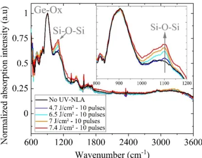
Fast and non-destructive optical spectroscopy methods (FTIR and PL) were initially used to investigate impurity-related optical defects and their chemical bonds formed during the laser annealing process. Fig. 1 presents the absorption spectra of Si-epi samples laser annealed in air with energy densities between 4.7 and 7.4 J/cm² and 10 pulses. The peak located at ~900 cm-1, observed in all investigated samples, is related to a Ge-Ox defect originating from the germanium ATR accessory. The main difference between the measured spectra occurs at ~1100 cm-1, where a peak related to a Si-O-Si region is observed (cf. inset inFig. 1) [14]. The Si-O-Si signal is already present in the reference non-annealed sample, due to the interstitial oxygen atoms already present in the epilayer (with a concentration of ~1x1016 cm-3). However the peak intensity (i.e. the concentration of the corresponding interstitial oxygen atoms) increases when the laser energy increases, clearly indicating that the formation of this complex is enhanced by the laser annealing process. No other peaks are observed in the annealed samples.
The PL spectra obtained at 50 K with an excitation wavelength of 488 nm and a power of 2 mW on the reference non-annealed sample and the annealed samples with energy
densities between 2 and 8 J/cm² with 10 pulses are presentedinFig. 2. The non-annealed sample spectrum presents only one peak located at 1.07 eV which is the band-to-band transition of silicon (Si-BB) peak centered at 1.07 eV. This peak was used for normalizing spectra of different samples in order to compare PL emission. The non-normalized spectra from 0.78 up to 0.82 eV acquired with a higher excitation power (20 mW) are presented in the Fig.2 inset. The annealed samples exhibit a broad band extending from 0.78 to 1 eV and several additional peaks. Similarly to the FTIR observations, the intensity of this band
increases with the energy density of the laser beam, indicating an increase in the concentration of the related optical defects. Concerning their nature, the peaks centered at 0.97 and 0.79 eV can be safely attributed to the so-called G-line and C-line, which indicate that carbon and oxygen related defects are formed [15]. Indeed, the G emission is attributed to the presence of a Cs-Si-Ci complex with Cs and Ci corresponding to carbon atoms in substitutional and
interstitial sites, respectively; similarly, the C-line emission is attributed to a Ci-Oi complex representing a carbon atom in interstitial site interacting with an oxygen atom also in interstitial position. In the 0.89 - 0.96 eV energy range, we observe peaks on a broad unsymmetric band. These additional components arise from the recombination assisted by acoustic phonons. The large peak centered at 0.95 eV is related to the acoustic transverse phonon replica G(TA) and the sharper line at 0.89 eV, the so-called E line, to local mode of the G-line center [16, 17].
Figure 2. Normalized PL spectra obtained on Si-EPI samples: C-line, G-line and Si-BB are identified respectively at 0.79, 0.96 and 1.07 eV. Inset: Non-normalized spectra focalized on C-line at 0.79 eV and acquired with a higher excitation power. The star in inset represents a bench artefact.
FTIR and PL do not allow to compare the concentrations of C- and O-related defects, however they clearly highlighted their increase during the laser annealing at higher energy density. This could be due in principle to a redistribution, during the anneal, of the oxygen and carbon atoms already present in the substrate material, leading to a local increase of their concentration. Alternatively, the observed increase of C- and O-related defects can originate from the progressive incorporation of carbon and oxygen atoms from an external source during UV-NLA. In order to clarify this point, we etched the 8 J/cm² annealed sample at
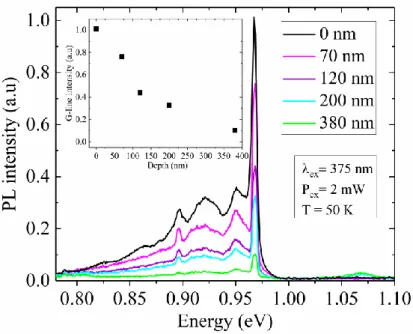
different depths (70, 120, 200 and 380 nm, as measured by mechanical profilometer) and observed the corresponding PL signal using a 375 nm laser, whose penetration depth in silicon is ~23 nm. The corresponding results are reported in Fig. 3, together with the signal recorded from a reference non-etched sample. For a reliable comparison of the experimental data, the acquisition parameters and the experimental conditions were strictly identical. All investigated samples exhibit similar PL spectra, including C-lines, G-lines and G-satellite lines. However, the intensity of all the defect-related peaks is found to decrease when increasing the etch depth, suggesting that the concentration of the elemental impurities responsible for their formation also decreases with depth, in agreement with an impurity in-diffusion mechanism from an external source. This conclusion is supported by the
corresponding increase in the intensity of the Si-BB peak (located at ~1.06 eV, cf Fig. 3) when increasing the etch depth, indicating that the contribution of the undamaged Si substrate to the overall PL spectrum becomes more prominent when the defect concentration decreases. This scenario is particularly obvious in the case of carbon, for which the intensity of the corresponding G-line peak decreases by a factor of about five when moving from the surface down to a depth of 380 nm (cf. inset of Fig. 3). In contrast, due to the weak intensity of the oxygen-related C-line peak, it is more difficult to confirm such conclusion in the case of oxygen.
Figure 3. PL spectra obtained on EPI sample annealed at 8 J/cm² and 10 pulses at different depth.
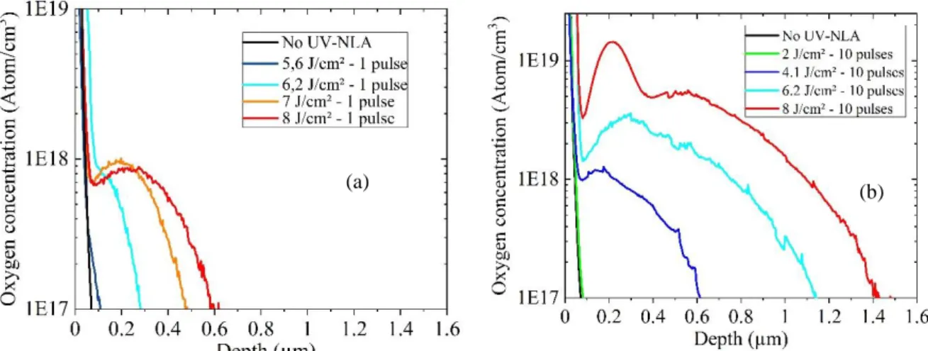
SIMS analyses were therefore carried out to further investigate the impurity distribution in UV-NLA annealed samples. Fig.4 depicts oxygen concentration profiles obtained on Si-epi samples without (black curve) and with UV-NLA at energy densities in the range 2 - 8 J/cm2 with 1 pulse (a) and 10 pulses (b). Clearly, for all the measured samples, the oxygen
concentration is higher in the surface region and decreases with depth, while both the total oxygen dose and the penetration depth increase with the laser energy density. These results therefore confirm that a progressive in-diffusion of oxygen from an external source occurs during UV-NLA, in agreement with previous literature reports [6, 18, 19]. Indeed, for the samples annealed with 1 laser pulse, the penetration depth is consistent with the known value of oxygen diffusivity in liquid silicon [20, 21]. As a consequence, oxygen atoms do not
laser pulses enables the in-diffused oxygen to diffuse near the maximum melt depths, which were estimated by phase field simulations [22] as 450 nm, 1000 nm and 1600 nm at 4, 6 and 8 J/cm², respectively (cf. Fig. 4b).
In addition, for the highest thermal budget investigated in this work (8 J/cm2 and 10 pulses), an immobile peak is observed in the oxygen profile at ~200 nm below the surface. This is probably due to the formation of oxygen-related precipitates. Indeed, the immobile peak is observed at concentrations above ~5x1018 cm-3, which corresponds to the known solubility limit of oxygen in liquid silicon [21, 23, 24].
Finally, for all the investigated samples, the oxygen concentration profile is found to decrease in the proximity of the sample surface. Such depletion could be ascribed to a variety of phenomena. However, considering that the equilibrium distribution coefficient of oxygen is very close to unity [25], oxygen segregation at the liquid/solid interface during solidification can be excluded. Similarly, the exact nature of the source of oxygen in-diffusion, i.e. either finite or infinite, cannot be responsible for the observed shape of the concentration profile, as in both cases the expected maximum should be located at the surface. In contrast, oxygen adsorption at the liquid/solid interface during annealing could explain the observed results. Indeed, such interface segregation mechanism (whereas the impurity is adsorbed by the moving interface from both the liquid and the solid phase) has been successfully used to simulate similar surface depletion effects in laser annealed boron-doped Silicon [26, 27], however further experiments would be necessary to confirm this scenario and a clear explanation cannot be reached at this stage.
Figure 4. SIMS profiles of oxygen concentration in depth generated by laser annealing for various density energy and (a) 1 pulse or (b) 10 pulses.
Carbon depth profiles from annealed samples with energy densities in the 3.2 – 8 J/cm2 range and 10 pulses were also measured by SIMS and the non-calibrated results are reported in Fig. 5. A reference non-annealed (black curve) sample was included in the measurement. As it appears from this figure, the annealed samples present a gradual decrease of carbon count from the surface down to the maximum melted depth, in agreement with the PL results presented in Fig. 5. Similarly to oxygen, carbon in-diffusion from an extenal source occurs during laser annealing. In contrast, no carbon precipitation is observed in any of the
investigated samples. This suggests that, independently of the laser energy density value, the maximum carbon concentration never exceeds its solubility value in liquid silicon (estimated to be ~3.5.1017 cm-3 [21, 28]).
(b) (a)
Figure 5. SIMS depth profiles of carbon in reference and annealed samples at various laser energy densities.
3.2 Impurities penetration mechanism
The results shown in the previous section confirm that a progressive in-diffusion of oxygen from an external source occurs during UV-NLA at high energy densities. However, compared to the widely investigated low energy density anneals, the physical mechanism governing oxygen penetration might be strongly modified and should therefore be
investigated. As a starting point, we focused on the identification of the main source from which the in-diffused oxygen atoms originate. To this purpose, two Si-epi samples were annealed under vacuum (~10-4 mbar) at an energy density of 4 J/cm² and 1 pulse. One sample was covered by a natural native oxide of ~1 nm (sample “Native oxide”), the other received a SF6 plasma etch in the laser chamber before the anneal (sample “SF6-pretreat”) which
resulted in the complete removal of the surface oxide layer. The oxygen SIMS profiles from these samples are shown in Fig. 6 (a), together with a SIMS profile from a reference “Native
oxide” sample that received no treatment (i.e. no UV-NLA, no surface oxide removal).
Calibration standards were not available for these measurements, the results are therefore reported in arbitrary units. The “Native oxide” annealed sample (cf. blue line in Fig. 6a) clearly exhibits oxygen penetration down to ~300 nm, similarly to the “Si-epi” samples annealed in air ambient (cf. Fig. 4) which also contained a ~1 nm-thick native oxide at the surface. Considering the absence of oxygen in the annealing ambient when UV-NLA is carried out in vacuum, this result clearly indicates that a natural native oxide can act as a source of oxygen penetration during annealing. This conclusion is confirmed by the result obtained from the “SF6-pretreat” sample, in which the native oxide was completely removed
prior to anneal (cf. green line in Fig. 6a). Indeed, this sample showed no oxygen penetration, similarly to the reference non-annealed sample (cf. black line). In contrast, any sulfur atoms left on the sample surface following the SF6 plasma treatment, are expected to penetrate and diffuse in the Si substrate during the laser annealing process, which is confirmed by the SIMS profile reported in Fig. 6 (b).
Figure 6. (a) SIMS profiles of oxygen obtained on the samples annealed in vacuum atmosphere at 4 J/cm² and 1 pulse with and without SF6 plasma treatment, (b) SIMS profiles of sulfur obtained on sample etched then annealed
In a subsequent experiment, we investigated the impact of the annealing ambient on the observed oxygen penetration. Figure 7 reports the oxygen depth profiles from two Si-Cz “native oxide” samples which were annealed at an energy of 4 J/cm2 (10 pulses) under different ambients: air (blue curve) and flowing N2 (red). If a contribution to the in-diffused oxygen atoms is to be expected from the annealing atmosphere, a deeper penetration should be observed in the sample annealed in air. Instead, the two samples exhibit the same oxygen profile, independently of the amount of oxygen atoms contained in the annealing atmosphere. This is in agreement with the previous result (cf. Fig. 6), confirming that the in-diffused oxygen atoms observed in these experiments originate from the native oxide layer.
It has to be noted that the results shown here, obtained from Si-Cz samples, are similar to those obtained from Si-epi samples annealed under the same laser conditions, as confirmed by the additional oxygen profile reported in Fig. 7 (green curve), measured from a Si-epi sample annealed in air. The only difference between Si-epi and Si-Cz samples is given by the oxygen trapping peak located at the maximum melt depth (~500 nm), which is only observed in the Si-CZ sample. The formation of this trapping peak might be due to the interaction of the in-diffused oxygen atoms with the excess point defects generated at the maximum melt depth [29] as well as with C impurities already present in the substrate (whose concentration is much higher in Si-CZ wafers compared to Si-epi ones [30]).
Figure 7. SIMS profiles of oxygen concentration obtained on the samples annealed at 4 J/cm² and 10 pulses in ambient air in epitaxial layer (green curve) and in CZ sample (blue curve) and under nitrogen flow in CZ sample (red curve).
In a final experiment, we investigated a set of three CZ samples (“HF-pretreat”, “Native oxide” and “Thermal oxide”, cf. section 2.1) with different thicknesses of the surface oxide (~0.3, ~1 and 4 nm, respectively) and annealed under the same laser conditions (3.6 J/cm² and 10 pulses). The oxygen profiles measured from the three samples are reported in Fig. 8(a), which also includes a profile measured from a reference non-annealed sample (No-UV-NLA). Similarly to the previous case, all annealed samples exhibit the same oxygen depth profiles, with the exception of a slightly increase of the melt depth for the “Thermal oxide” sample (probably due to a modification of the optical absorption in the presence of a thicker surface oxide layer) and the absence of the oxygen trapping peak at the maximum melt depth. Not only this result confirms that the observed oxygen penetration originates from the surface oxide layer, but it also indicates that the amount of in-diffused oxygen does not depend on its thickness, suggesting that the O atoms are released from a very small region in the vicinity of the SiO2/Si interface.
Carbon depth profiles measured from the same samples are reported inFig. 8(b). While the “HF-pretreat” and “Native oxide” samples exhibit a similar carbon penetration to that previously observed in Si-epi samples (cf. Fig. 5), no carbon penetration is observed in the “Thermal oxide” sample (green curve in Fig. 8(b)). Indeed, the formation of the surface oxide in “HF-pretreat” and “Native oxide” samples is a “natural” process during which C contaminants are trapped in the oxide layer. Thus, when carbon atoms are trapped at the SiO2/Si interface during the oxide formation, they are released during UV-NLA (similarly to oxygen) and diffuse in the melted and recrystallized layer. In contrast, the surface oxide of the “Thermal oxide” sample is formed at 800 °C (and preceded by a SC1 cleaning step). This is a much cleaner process leading to the formation of a perfect, C-free, SiO2/Si interface, in agreement with the absence of carbon penetration in this sample (cf. Fig. 8(b)). In addition, the annealing step necessary for the formation of the thermal oxide can induce an outdiffusion of carbon from the CZ silicon substrate [31]. This might explain the absence of the oxygen trapping peak at the maximum melt depth for this sample (cf. Fig 8(a)).
Figure 8. SIMS profiles of oxygen concentration (a) and carbon (b) obtained on the samples annealed at 3.6 J/cm² and 10 pulses with different surface states: 1 nm native oxide (blue), 0.3 native oxide (red) and 4 nm thermal oxide (green).
All the results presented so far clearly show that the observed oxygen penetration during high energy density UV-NLA originates from the surface oxide layer. In addition, they suggest that the in-diffused O atoms are released from a very small region in the vicinity of the SiO2/Si interface. In order to further investigate this last point, we extracted (from the SIMS depth profiles) the total areal density of in-diffused O atoms (hereafter “O dose”) in all the measured samples. In particular, for the sample that received the highest thermal budget (8 J/cm2 and 10 pulses) the in-diffused O dose is ~6x1013 cm-2. This is much lower (~20 times less) than the oxygen areal density contained in a single mono-layer (ML) of stoichiometric SiO2 (~1.25x1015 cm-2), whose thickness is ~0.3 nm [32]. Thus, it can be reasonably assumed that, during melt UV-NLA at high energy densities, the prolonged contact of SiO2 with high temperature liquid Si(> 1600 °C) induces a partial degradation of the SiO2/Si interface, leading to some bond breaking and subsequent injection of O atoms into the substrate. Indeed, a degradation implying no more than 5 % of the O atoms contained in the 1st SiO2 ML is sufficient to account for the measured amount of in-diffused O in all analysed samples. For the highest laser energies used in this work (up to 8 J/cm2) it cannot be excluded that the native SiO2 undergoes an abrupt glass-liquid transition at very high temperature. In such case, a much higher amount of oxygen atoms would be available for diffusing into the substrate. However, the maximum oxygen concentration at the surface would still be determined by its solubility limit in liquid silicon (~5x1018 cm-3), in agreement with the observed values (cf. Fig. 4b). Whether or not SiO2 achieves a liquid state at the highest laser energies, the proposed scenario is also consistent with the observed C in-diffusion in samples where C contaminants are trapped at the SiO2/Si interface prior to UV-NLA (cf. Fig. 8b) [33]. Indeed, in such samples, the degradation of the SiO2/Si interface can lead to the concomitant release of both O and C atoms. Although based on a different physical mechanism, it is interesting to note that SiO2/Si interfacial degradation was already identified as the cause of oxygen in-diffusion during high temperature furnace annealing (up to 1320 °C, i.e. below melt) [33, 34].
The oxygen penetration investigated in this work is active only when the laser energy density is sufficiently high. For a 308 nm laser radiation with a 160 ns pulse duration, the estimated energy threshold is ~5.6 J/cm2 for 1 pulse anneals, or between 2 and 4 J/cm2 for 10 pulse anneals. Below this threshold, oxygen penetration is totally absent or negligible, in agreement with previous investigations at lower laser energies and inert ambient [35]. In that energy regime, O penetration was only observed when anneal occurred in pure O2 ambient
either at atmospheric pressure [36] or at high pressure (4 atm [37]). This explains why in low energy conditions, any surface oxide layer (native or grown), present during UV-NLA, would act as a barrier to oxygen penetration. On the contrary, concerning the high energy regime investigated in this work, the surface SiO2 layer acts as the source of the in-diffused oxygen. For application of NLA in the power device domain, surface oxide removal prior to UV-NLA is mandatory if oxygen (and carbon) contaminations must be avoided.
4. Conclusions
In this work, we presented a comprehensive investigation of impurity contamination in silicon during melt laser annealing at high energy density by implementing a methodology allowing the identification of formed defects and the localization of the in-diffused impurities. FTIR, photoluminescence spectroscopy and SIMS measurements confirm that a progressive in-diffusion of oxygen from an external source occurs during UV-NLA at high energy densities. By investigating in detail the impact of the annealing ambient and of the surface preparation prior to UV-NLA (including the variation of the surface oxide thickness), we showed that the source of the in-diffused oxygen is the surface oxide layer. It is proposed that, at high energy UV-NLA, the prolonged contact of SiO2 with high temperature liquid Si induces a partial degradation of the SiO2/Si interface, leading to bond breaking and
subsequent injection of O atoms into the substrate. Indeed, a degradation implying no more than 5 % of the O atoms contained in the 1st SiO
2 ML is sufficient to account for the measured amount of in-diffused O in all of the analysed samples.
5. Acknowledgments
The research leading to these results has received funding from the European Union's Horizon 2020 research and innovation program under grant agreement N°871813
MUNDFAB. We thank the Raimond Castaing micro-characterisation platform of Toulouse and the Géosciences laboratory of Montpellier for performing the SIMS measurements. We also thank the engineers of the I2C characterization platform of LAAS-CNRS for their support.
References
[1] K. Huet, F. Mazzamuto, T. Tabata, I. Toqué-Tresonne, and Y. Mori, Doping of semiconductor devices by Laser Thermal Annealing, Materials Science in Semiconductor Processing 62 (2017) 92–102.
https://doi.org/10.1016/j.mssp.2016.11.008
[2] T. Sarnet, M. Hernandez, and D. Débarre, “Dopage laser en microélectronique,” Journal de Physique IV 138 (2006) 203–212. https://doi.org/10.1051/jp4:2006138023
[3] D.H. Lowndes, J. W. Cleland, W. H. Christie, R. E. Eby, G. E. Jellison Jr., J. Narayan, R. D. Westrbrook, R. F Wood, J. A. Nilson and S. C. Dass, Pulsed excimer laser annealing of ion implanted silicon: Characterization and solar cell fabrication, Applied Physics Letters 41 (1982) 938-940. https://doi.org/10.1063/1.93342
[4] P. G. Carey, K. Bezjian, T. W. Sigmon, P. Gildea, and T. J. Magee, Fabrication of Submicrometer MOSFET’s Using Gas Immersion Laser Doping (GILD), IEEE Electron Device Letters 7 (1986) 440-442. https://doi.org/10.1109/EDL.1986.26429
[5] R. Nipoti, M. Bianconi, R. Fabbri, M. Servidori, S. Nicoletti, and R. Canteri, Electrical and structural characterization of silicon layers directly doped with boron by excimer
laser irradiation, Applied Surface Science 43 (1989) 321–324. https://doi.org/10.1016/0169-4332(89)90233-X
[6] K. Hoh, H. Koyama, K. Uda, and Y. Miura, Incorporation of Oxygen into Silicon during Pulsed-Laser Irradiation, Japanese Journal of Applied Physics 19 (1980) 375-378. https://doi.org/10.1143/JJAP.19.L375
[7] G.G. Bentini, M. Berti, C. Gohen, A.V. Drigo, E. Iannitti, D. Pribat and J. Siejka, Effect of oxygen pressure on oxygen incorporation in Si and Ga As during Q switched laser irradiation, Journal de Physique C1 (1982) 229-234.
https://doi.org/10.1051/jphyscol:1982131
[8] M. Berti, L. F. Doná dalle Rose, A. V. Drigo, C. Cohen, J. Siejka, G. G. Bentini and E. Jannitti, Matrix atomic losses and oxygen incorporation under ruby-laser irradiation of silicon in gaseous atmospheres, Physical Review B 34 (1986) 2346.
https://doi.org/10.1103/PhysRevB.34.2346
[9] C. Fenouillet-Beranger, B. Mathieu, B. Previtali, M-P. Samson, N. Rambal, V. Benevent, S. Kerdiles, J-P. Barnes, D. Barge, P. Besson, R. Kachtouli, P. Batude, M. Cassé, X. Garros, A. Laurent, F. Nemouchi, K. Huet, I. Toqué-Trésonne, D. Lafond, H. Dansas, F. Aussenac, G. Druais, P. Perreau, E. Richard, S. Chhun, E. Petitprez, N. Guillot, F. Deprat, L. Pasini, L. Brunet, V. Lu, C. Reita and M. Vinet, New insights on bottom layer thermal stability and laser annealing promises for high performance 3D VLSI, IEEE International Electron Devices Meeting (2014).
https://doi.org/10.1109/IEDM.2014.7047121
[10] M. Rahimo, C. Corvasce, J. Vobecky, Y. Otani, and K. Huet, Thin-Wafer Silicon IGBT With Advanced Laser Annealing and Sintering Process, IEEE Electron Device Letters 33 (2012) 1601-1603. https://doi.org/10.1109/led.2012.2215304
[11] S. Gupta, B. Pecholt, and P. Molian, Excimer laser ablation of single crystal 4H-SiC and 6H-SiC wafers, Journal of Materials Science 46 (2011) 196-206.
https://doi.org/10.1007/s10853-010-4920-7
[12] T. Tabata, S. Halty, I. Toqué-Trésonne, F. Mazzamuto, K. Huet, and Y. Mori, UV excimer laser annealing for next generation power electronics, 21st International Conference on Ion Implantation Technology (IIT), Tainan, (2016).
https://doi.org/10.1109/IIT.2016.7882917
[13] K. Huet, J. Aubina, P.-E. Raynal, B. Curvers, A. Verstraete, B. Lespinasse, F.
Mazzamuto, A. Sciutob, S.F. Lombardo, A. La Magna, P. Acosta-Alba, L. Dagault, C. Licitra, J.-M. Hartmann, S. Kerdilès, Pulsed laser annealing for advanced technology nodes: Modeling and calibration, Appl. Surf. Sci. 505, 144470 (2020),
https://doi.org/10.1016/j.apsusc.2019.144470
[14] V. P. Tolstoy, I. V. Chernyshova and V. A. Skryshevsky, Handbook of Infrared Spectroscopy of Ultrathin Films, Wiley/Interscience, Hoboken (2003).
[15] M. Tajima, H. Kiuchi, F. Higuchi, and A. Ogura, Quantification of C in Si by
photoluminescence at liquid N temperature after electron irradiation, Applied Physics Express 10 (2017) 046602. https://doi.org/10.7567/APEX.10.046602
[16] K. Thonke, H. Klemisch, J. Weber, and R. Sauer, New model of the irradiation-induced 0.97-eV (G) line in silicon: A Cs-Si* complex, Physical Review B 24 (1981) 5874.
[17] R. Monflier, H. Rizk, T. Tabata, J. Roul, S. Boninelli, M. Italia, A. La Magna, F. Mazzamuto, P. Acosta Alba, S. Kerdiles, F. Cristiano, and E. Bedel-Pereira, Defects Investigation in Nanosecond laser Annealed Crystalline Silicon: Identification and Localization, 22nd International Conference on Ion Implantation Technology (IIT), Würzburg, Germany, (2018) 132-135. https://doi.org/10.1109/IIT.2018.8807933
[18] M. Ametowobla, G. Bilger, J. R. Köhler and J. H. Werner, Laser induced lifetime degradation in p-type crystalline silicon, Journal of Applied Physics 111 (2012), 11, 114515, https://doi.org/10.1063/1.4725191
[19] Z. Hameiri, T. Puzzer, L. Mai, A. B. Sproul, S. R. Wenham, Laser induced defects in laser doped solar cells, Photovolt: Res. Appl 19 (2011) 391–405,
https://doi.org/10.1002/pip.1043
[20] A. Giannattasio, J. D. Murphy, S. Senkader R. J. Falster, and P. R. Wilshaw, Oxygen and Nitrogen Transport in Silicon Investigated by Dislocation Locking Experiments, journal of The Electrochemical Society 152 (2005) 460-467. https://doi.org/
10.1149/1.1901669
[21] P. Pichler, Intrinsic Point Defects, Impurities, and Their Diffusion in Silicon, Springer, Vienna (2004).
[22] S.F. Lombardo, G. Fisicaro, I. Deretzis, A. La Magna, B. Curver, B. Lespinasse, K. Huet, Theoretical study of the laser annealing process in FinFET structures, Applied Surface Science 467-468 (2019) 666-672. https://doi.org/10.1016/j.apsusc.2018.10.155 [23] Y. Yatsurugi, N. Akiyama, Y. Endo and T. Nozaki, Concentration, Solubility, and
Equilibrium Distribution Coefficient of Nitrogen and Oxygen in Semiconductor Silicon, Journal of The Electrochemical Society 120 (1973) 975-979.
https://doi.org/10.1149/1.2403610
[24] T. Narushima, K. Matsuzawa, Y. Mukai and Y. Iguchi, Oxygen Solubility in Liquid Silicon, Materials Transactions 35 (1994) 522-528.
https://doi.org/10.2320/matertrans1989.35.522
[25] T. Narushima, A.Yamashita, C. Ouchi and Y. Iguch, Solubilities and Equilibrium Distribution Coefficients of Oxygen and Carbon in Silicon, Materials Transactions, 43(8) (2002) 2120-224. https://doi.org/10.2320/matertrans.43.2120
[26] M. Hackenberg, K. Huet, R. Negru, J. Venturini, G. Fisicaro, A. La Magna, P. Pichler, Modeling boron profiles in silicon after pulsed excimer laser annealing, AIP Conf. Proc. 1496 (2012) 241.http://dx.doi.org/10.1063/1.4766533
[27] G. Fisicaro, K. Huet, R. Negru, M. Hackenberg, P. Pichler, N. Taleb, and A. La Magna, Anomalous Impurity Segregation and Local Bonding Fluctuation in l-Si, Phys. Rev. Lett. 110 (2013) 117801, https://doi.org/10.1103/PhysRevLett.110.117801
[28] T. Nozaki, Y. Yatsurugi and N. Akiyama, Concentration and Behavior of Carbon in
Semiconductor Silicon, Journal of The Electrochemical Society 117 (1970) 1566-1568.
[29] G. Mannino, V. Privitera, A. La Magna, E. Rimini, E. Napolitani, G. Fortunato, and L. Mariucci, Depth distribution of B implanted in Si after excimer laser irradiation, Applied Physics Letters 86 (2005) 051909. https://doi.org/10.1063/1.1856696
[30] S. Nakagawa, and K. Kashima, Quantitative analysis of carbon impurity concentration in silicon epitaxial layers by luminescence activation using carbon ion implantation and
electron irradiation, Phys. Status Solidi C 11 (2014) 1597-1600. https://doi.org/10.1002/pssc.201400046
[31] F. Shimura, and T. Higuchi, Outdiffusion of oxygen and carbon in Czochralski silicon, Appl. Phys. Lett. 53 (1988) 69-71. http://dx.doi.org/10.1063/1.100126
[32] R.A.B. Devine, SiO2/Si Interfacial Degradation and the Role of Oxygen Interstitials, J. Phys. III France 6 (1996) 1569-1594, https://doi.org/10.1051/jp3:1996203
[33] O. Senftleben, H. Baumgärtner, and I. Eisele, Cleaning of Silicon Surfaces for Nanotechnology, Materials Science Forum Vols. 573-574 (2008) 77-117. https://doi.org/ 10.4028/www.scientific.net/MSF.573-574.77
[34] R.A.B. Devine and D. Mathiot, O interstitial generation and diffusion in high temperature annealed Si/SiO2/Si structures, Journal of Applied Physics 79, 2302 (1996), https://doi.org/10.1063/1.361155
[35] M. Berti, L. F. Doná dalle Rose, A. V. Drigo, C. Cohen, J. Siejka, G. G. Bentini, and E. Jannitti, Matrix atomic losses and oxygen incorporation under ruby-laser irradiation of silicon in gaseous atmospheres, Phys. Rev. B 34, 2346 (1986),
https://doi.org/10.1103/PhysRevB.34.2346
[36] G.G. Bentini, M. Berti, C. Gohen, A.V. Drigo, E. Tannitti, D. Pribat and J. Siejka, Effect of oxygen pressure on oxygen incorporation in Si and GaAs during Q switched laser irradiation, Journal de Physique, Colloque Cl, supplément au n° 10, 43 (1982) C1-229
[37] K. Hoh, H.Koyama, K. Uda and Y. Miura, Incorporation of Oxygen into Silicon during Pulsed-Laser Irradiation, Japanese Journal of Applied Physics, 19 (1980) 7, L375-L378