HAL Id: hal-01423144
https://hal.inria.fr/hal-01423144
Submitted on 28 Dec 2016
HAL is a multi-disciplinary open access
archive for the deposit and dissemination of
sci-entific research documents, whether they are
pub-lished or not. The documents may come from
teaching and research institutions in France or
abroad, or from public or private research centers.
L’archive ouverte pluridisciplinaire HAL, est
destinée au dépôt et à la diffusion de documents
scientifiques de niveau recherche, publiés ou non,
émanant des établissements d’enseignement et de
recherche français ou étrangers, des laboratoires
publics ou privés.
UTBB FDSOI suitability for IoT applications:
Investigations at device, design and architectural levels
Florent Berthier, Edith Beigné, Frédéric Heitzmann, Olivier Debicki,
Jean-Frédéric Christmann, Alexandre Valentian, Olivier Billoint, Esteve
Amat, Dominique Morche, Soundous Chairat, et al.
To cite this version:
Florent Berthier, Edith Beigné, Frédéric Heitzmann, Olivier Debicki, Jean-Frédéric Christmann, et al..
UTBB FDSOI suitability for IoT applications: Investigations at device, design and architectural levels.
Solid-State Electronics, Elsevier, 2016, 125, pp.14 - 24. �10.1016/j.sse.2016.09.003�. �hal-01423144�
UTBB FDSOI Suitability for IoT Applications : Investigations at
Device, Design and Architectural Levels
Florent Berthiera,b,∗, Edith Beignea, Fr´ed´eric Heitzmanna, Olivier Debickia, Jean-Fr´ed´eric Christmanna, Alexandre Valentiana, Olivier Billointa, Esteve Amata,
Dominique Morchea, Soundous Chairata, Olivier Sentieysb,
aCEA Leti - MINATEC, 17 rue des Martyrs, 38054 GRENOBLE CEDEX 9, France bIRISA/INRIA, University of Rennes 1, 6 rue Kerampont BP80518 - 22305 Lannion Cedex, France
Abstract
In this paper, we propose to analyze Ultra Thin Body and Box FDSOI technology suitability and architectural solutions for IoT applications and more specifically for autonomous Wireless Sensor Nodes (WSNs). As IoT applications are extremely diversified there is a strong need for flexible solutions at design, architectural level but also at technological level. Moreover, as most of those systems are recovering their energy from the environment, they are challenged by low voltage supplies and low leakage functionalities. We detail in this paper some Ultra Thin Body and Box FDSOI 28nm characteristics and results demonstrating that this technology could be a perfect option for multidisciplinary IoT devices. Back biasing capabilities and low voltage features are investigated demonstrating efficient high speed/low leakage flexibility. In addition, architectural solutions for WSNs microcontroller are also proposed taking advantage of Ultra Thin Body and Box FDSOI characteristics for full user applicative flexibility. A partioned archi-tecture between an Always Responsive part with an asynchronous Wake Up Controller (WUC) managing WSN current tasks and an On Demand part with a main processor for application maintenance is presented. First results of the Always Responsive part implemented in Ultra Thin Body and Box FDSOI 28nm are also exposed.
Keywords: UTBB FDSOI, IoT, Asynchronous Processor, Power Estimation, MCU 2016 MSC:,
1. Introduction
The Internet of Things is supposed to encompass billions of connected devices. Among them, Wireless Sensor Nodes (WSN) are distributed and communicate through a network. They are able to measure physical or environmental conditions while transferring data through RF com-munication. Versatility and energy management are key concerns for those objects handling many different applications and requiring different performances in an autonomous way (Figure 1). In such ultra-low energy applications, autonomous WSNs have to cope with new constraints
∗Corresponding author. Tel.:+33 4 38 78 26 21
Email address: [email protected] (Florent Berthier)
like changing energetic environment, long idle phases, automatic wake up, data back-up when the system is unexpectedly turned off, and ultra-low voltage operation.
Figure 1: IoT applications (examples): performance and energy needs
Well-known applications of the Internet of Things are requiring low performances (1-100MHz) and ultra-low leakage. They are thus using technology nodes from 180nm down to 65nm [1] [2]. This choice is justified by both cost and leakage power as those systems are most of their time asleep and wake up only once in a while [3]. As a result, leakage power reduc-tion during idle phases is crucial. Nevertheless, such technologies are limiting the overall speed performances of an IoT system during computing phases restraining their field of applications. Indeed, it would be highly relevant, for the WSN, to be able to compute or transfer data at high speed if a large amount of energy is harvested in the environment. It would thus widen the applicative scope and enable new flexible applications requiring different performances level according to energetic environment.
In this context, we propose in this work to bring flexibility to smart devices by using both some technological and architectural solutions. At technology level, we propose to take advan-tage of UTBB FDSOI (Ultra Thin Body and Box FDSOI) technology providing a wide range of tunability between high speed and low leakage [4]. Undoped thin-film planar FDSOI is an alternative to bulk devices at the 28nm node and beyond and exhibits an excellent short-channel electrostatic control, low leakage currents and immunity to random dopant fluctuation. This technology allows the designers to meet the needs of autonomous low power devices, combining high performance and low power consumption while demonstrating very good performances at low supply voltages. This is possible through the use of an effective Back Biasing (BB) allow-ing to dynamically switch between high performance mode (Forward Back Biasallow-ing) or ultra-low leakage mode (Reverse Back Biasing). However, as the technology cannot do all the job, a new versatile sub-system microcontrollers architectures is also proposed to fit a largest number of IoT applications as shown in Figure 1. Many smart devices or sub-system microcontrollers have been proposed [2], [5], [6], [7], [8] but they are covering only small segments of the speed/power performance spectrum required by IoT applications. Today, more and more applications are re-quiring both high performance for highly computational tasks and very low power consumption for simple tasks.
In this paper we propose to investigate UTBB FDSOI technology at device, design and archi-tectural levels to propose flexible smart devices for IoT applications. Firstly, in Section 2, we discuss flexibility requirements for IoT devices. UTBB FDSOI advantages for Wireless Sensor
Nodes at device level are highlighted in Section 3 by detailing back biasing options and suit-ability at near-threshold voltage. Then, architectural level solutions for flexible smart device are presented in Sections 4, 5 and 6. Section 4 is demonstrating the power efficiency of a partitioned architecture and Sections 5 and 6 present architecture details and UTBB FDSOI implementation results.
2. Flexibility Requirements for IoT Devices
The Internet-of-Things is addressing many different applications and it is not possible to come up with a single speed and power target out of them. In autonomous Wireless Sensor Nodes, energy levels considered can cover from the pW up to the mW range (Figure 1). A simple tracking and monitoring application will require less power than a smart camera for vision ap-plications. Moreover, if we consider sensor data fusion applications, their energy needs can differ considerably. 1-bit level crossing detection can be simply required for a basic wake-up scheme but also very high conversion accuracy can be requested for a more complex sensor acquisition application. Moreover, if we consider wireless sensor nodes distributed in our envi-ronment, it is noticeable that they will be target multiple applications and probably also multiple communication-standard. In any case, a high versatility is mandatory at architectural, design and technological levels. At design level, many solutions are emerging today using adaptive mixed-signal and digital blocks and their associated control.
Devices of the Internet-of-Things are also known to be in idle mode most of their lifetime. It is thus required to have circuits consuming very low leakage power to save the battery lifetime or increase the system autonomy. In that sense, at design time, low leakage technological options are chosen and fixed for the circuit, limiting their overall speed performances. Circuits are then suffering from very low throughput even if not is enough energy is available to perform more complex tasks. UTBB FDSOI technology allows finding a compromise between high speed and low leakage as we demonstrated in [4]. This is possible through the use of back biasing voltage as shown in section 3.1 of this paper.
Another issue to be discussed is regarding energy harvesting. This new autonomous power supply scheme is bringing more challenges to the circuit. In fact, autonomous wireless sensor nodes which are recovering their energy from the environment can be affected by varying en-ergetic environments. This will result in a variable energy level available for the node over the time. This power delivery system imposes on the node a need to remain functional at different voltage supplies and even more at very low voltage levels down to threshold. In modern tech-nologies, low voltage supplies presupposes very low speed performance and can compromise the applicative task completion. This is the reason why UTBB FDSOI back biasing capability will be used to boost the performance of the circuit for a given task even if the voltage supply is low. This is demonstrated in Section 3.2.
By definition, a smart device is able to sense, communicate and manage its own power supply. Those systems are thus mixed-signal circuits using RF transceivers, sensor and data converters, image sensors, voltage converters and other analog blocks. Full integration is thus an issue as it is impossible to find a common technology fitting analog and digital requirements [5]. Todays smart devices are generally integrated in-package using different technologies and sensors. It leads to a lack of global optimization as different part of the node are designed into different technologies and circuits. Due to its easy Vth modulation, UTBB FDSOI presents the great of being very suitable to analog designers. UTBB FDSOI can thus help a full integration of
digital and analog sub-modules by (1) maintaining the digital performance needs and (2) allowing efficient analog design.
After technological considerations, at architectural level, the smart device architecture also needs to be reconsidered for flexibility. Some industrial [7] [8] or academic [2] [5] [6] smart devices have been proposed, but targeting specific performances without providing a full ap-plicative range capability. In [5], a full system is proposed in 180nm technology exhibiting only 15nW in standby and 304nW dynamic power for a motion detection application. This exam-ple perfectly covers the ultra-low energy segment of Figure 1. For higher performance needs, STM32L0 microcontroller [7] is demonstrating 0.27 µA in standby and 139 µA/MHz (running at 32 MHz) and TI CC2650 [8] discloses 1 µA in standby and 6mA in transmission mode (RX/TX). However, none of these proposals are able to cover the full range of performances mainly due to technological and architectural limitations.
After discussing, in this section, the main advantages of using UTBB FDSOI 28nm technology node for IoT and the need for flexible architectures, we will, in the next section, focus on the use of (1) back biasing and its efficiency on speed and power modulation (2) FDSOI suitability at low voltage and even at near threshold computing.
3. UTBB FDSOI Characteristics for IoT Flexibility 3.1. UTBB FDSOI Back Biasing For High Flexibility
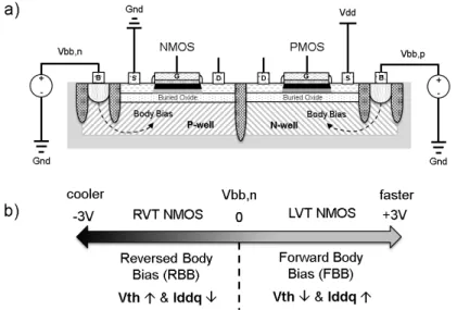
UTBB FDSOI 28nm ((Fig. 2(a)) is a high-k metal gate planar technology [4]. There is no channel doping nor pocket implant making the process simpler than bulk and reducing the vari-ability. To allow a good trade-off between drain/source-to-substrate parasitic capacitance and body factor, the Buried oxide (Box) thickness is 25nm. A back plane, either N-well (n-type) or P-well (p-type), is implemented under the buried oxide to improve the short channel effect and adjust the voltage threshold. Back bias polarization is feasible by removing a slice of the Box and finally, Shallow Trench Isolation (STI) is used to electrically isolate the devices.
Figure 2: UTBB FDSOI technology: (a) transistor cross section and (b) back biasing
A wide back biasing voltage range (+/-1.8V) enables transistor threshold voltage adjustment and modify the leakage current accordingly in a range unattainable by conventional bulk technol-ogy (Fig. 2(b)). Indeed, in bulk technoltechnol-ogy back biasing voltage is limited to+/-300mV, due to drain and source diodes and the back biasing voltage is usually fixed after fabrication for process compensation. This UTBB FDSOI only feature allows a dynamic power/performance scaling in order to achieve the highest speed or the lowest power or the best tradeoff between them in a single circuit/device.
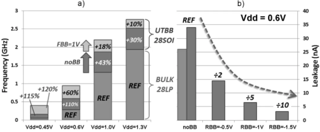
Figure 3a illustrates frequency boost results of UTBB FDSOI 28 nm compared with bulk technology at different power supply voltages. With a Forward Back Biasing (FBB) of 1V, UTBB FDSOI demonstrates very high speed gain from 43% at 1.3V up to 5X factor at 0.45V.
On the contrary, UTBB FDSOI enables to reduce leakage power consumption, when speed performance is not required, by applying Reverse Back Biasing (RBB) as shown Figure 3b. At 0.6V, leakage current could be divided by 2 at -0.5V RBB voltage and by 10 at -1.5V RBB voltage.
Figure 3: UTBB FDSOI performances extracted from ARM64 critical path electrical simulations (a) LVT performance boost with FBB (b) RVT Leakage reduction with RBB [10]
This back biasing scheme can push new Internet-of-Things applications requiring high speed performances during operation and ultra low leakage during standby phases. We would get rid of performance limitations encountered by old technology nodes while respecting leakage constraints during standby.
3.2. Exploring UTBB FDSOI at Near-Threshold Voltage
In this section, we study the impact of Back Biasing Voltage (VBB) on the Minimum Energy Point (MEP) operating point for Regular-VT (RVT) and Low-VT (LVT) UTBB FDSOI 28nm devices. As highlighted in Section 2, autonomous IoT devices recovering their energy form the environment can suffer from low voltage supplies. An interesting solution is to run at the Mini-mum Energy Point (MEP), defined as the operating voltage for which the total energy consumed per operation is minimized [2].
Results provided are extracted from electrical simulations of ring oscillators, adders and multi-pliers. In terms of methodology, this is common to use simple ring oscillators for exploring tech-nology performances. It allows to perform a large number of electrical simulations in different
Process, Voltage and Temperature conditions. For better correlation, critical path are simulated but this is out of the scope of this paper. Figure 4 demonstrates UTBB FDSOI flexibility and energy performance control. As expected, LVT devices demonstrate larger static energy than their RVT counterpart and this difference is increasing again when applying back biasing volt-age. While the total dynamic energy is not changing a lot with the back biasing voltage, static energy is substantially modified. An interesting property to note for IoT devices is that the MEP voltage value is not varying a lot with respect to RVT or LVT device and stands between 0.2V and 0.4V.
Figure 4: MEP analysis for RVT and LVT UTBB FDSOI ring oscillator under VBB variations. ZBB= no Body Biasing applied
If we compare leakage and energy results with a 28nm bulk technology and a 14 nm FinFET technology (Figure 5), it comes out that RVT UTBB FDSOI exhibits the lowest energy figures, although the lowest frequency (please note that FinFET results are based on predictive 14 nm models). Bulk 28nm technology demonstrates the worst overall performance with regard to FinFET and UTBB FDSOI.
Figure 5: Energy and Delay at MEP : comparison with bulk and FinFET technologies
In our scope of flexibility, even if FinFET demonstrates the best speed results, no back biasing is possible and performances are fixed at design time. UTBB FDSOI back biasing tuning will be used as an extremely efficient way to adapt the overall performance.
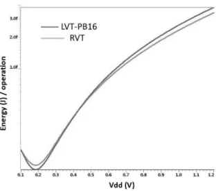
Another option, provided by UTBB FDSOI, is the use of Poly Biasing (PB) in the devices. It enables to enlarge the gate length and thus find a better energy/delay compromise. Various sizing optimizations were explored, i.e. modifying the beta-ratio and using the poly-biasing feature available in this technology, which emulates the increase of the transistor gate length by up to 16 nm. The use of an increased gate length was found to have a significant effect on the cell leakage and delay. However we have shown by simulations (Figure 6) that LVT PB16 (16nm gate increase) is also an interesting option at 0.5V voltage supply (Vdd).
Figure 6: Energy at MEP using Poly Biasing UTBB FDSOI options
At the minimum energy point, we observe an energy reduction about 15% by using PB16 with respect to a maximum frequency (500MHz). These energy savings can even go up to 25%, by reducing the frequency target by one order of magnitude. In terms of energy, we compare PB16 LVT performances with RVT UTBB FDSOI devices as shown on figure 6. LVT PB16 circuits could provide lower energy values than RVT-based ones while allowing a simplest co-integration with high speed LVT transistors.
In figure 7, we highlight an interesting behavior for our need for flexible IoT devices: while PB16 could be more suitable at sub-VT range, RVT devices entails lower energy consumption at higher Vdd (> 0.5V) when no VBB is applied. As it is difficult to co-integrate RVT and MVT cells due to Well isolation constraints, using LVT PB16 is a good compromise for low energy systems. It is thus worth pointing out that a LVT and LVT PB16 co-integration can be suitable for WSN applications requiring very high speed during operation and voltage supplies around 0.5V. On the other hand, if we consider lower performance wireless sensor nodes, functional in a wide voltage supply range and requiring less speed, they could perfectly be implemented by using RVT devices.
In this section, we have highlighted the UTBB FDSOI flexibility at device level using back biasing and its efficiency at low voltages. Other interesting properties, out of the scope of this paper, are RF analog results [9] and easy co-integration with non-volatile devices like PCRAM or MRAM [11]. In the next sections, we apply UTBB FDSOI advantages at design level and
Figure 7: LVT-PB16 and RVT energy results of ring oscillator on full Vdd range
propose an architectural solution to enhance the overall smart devices flexibility.
4. Microcontroller Architecture Characteristics for IoT Flexibility
As shown before, UTBB FDSOI is well suited for flexibility, but this issue has to be addressed at the architectural level too. A usual wireless sensor node has the architecture depicted in Figure 8. It is composed of five parts: (i) A radio module for packet transfer; (ii) multiple sensors for physical measurements; (iii) A microcontroller unit; (iv) A power management unit; (v) A battery and/or energy harvester for energy storing and scavenging.
Figure 8: Wireless sensor node architecture. Source: Renesas ASP-DAC 2014 [12]
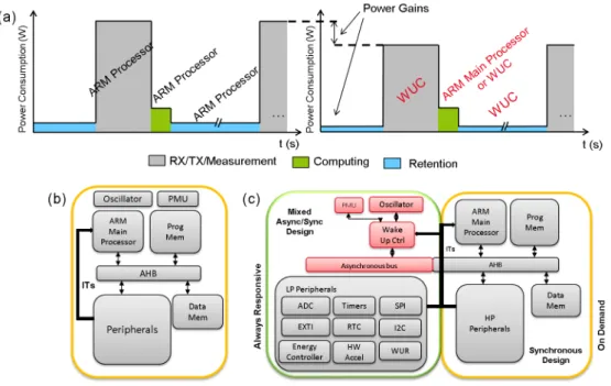
This section focuses on the power consumption reduction of the microcontroller sub-system by introducing new architectural solutions for high flexibility. A typical microcontroller archi-tecture is depicted on Figure 9b. In a regular wireless sensor node scenario, the microcontroller main processor is in charge of the three following tasks: data computation, data transfer and power management. However, current tasks such as simple measurements and data transfers are also performed by this processor, which represents a high power consumption for such simple
tasks. Therefore, to cover the full range of power and performances requirements as described in Section 2, we propose a partitioned architecture as presented on Figure 9c. This architecture is partitioned into two parts: An Always Responsive part including an ultra-low power processor, namely a Wake Up Controller (WUC), and an On Demand part integrating the main processor. The WUC is dedicated to the Wireless Sensor Node microcontroller current tasks, while the main processor manages the application part and the node maintenance. The Always Responsive part is a mixed asynchronous/synchronous design whereas the On Demand part is a pure synchronous design integrating a classical CPU (Cortex M for instance [6]).
A classical scenario for a wireless sensor node is divided into three phases as pictured in Figure 9a. During the retention phase, in a usual microcontroller, the main sub-modules are clock gated and the microcontroller is in the less power consuming mode, where only the wake up signals of the WSN node are active. In the reception/transmission/measurement phase (RX/TX/Measurement), the sensors or radio modules operate and perform data measurements or data wireless transfer. This phase period depends on the conversion accuracy of the sensor or on the radio protocol required for the application as well as on the number of data to be transferred. In the computing phase, the microcontroller is configured into its most power consuming mode to perform calculation on data. For our proposed microcontroller partitioned into a WUC and a main processor, each part can be called at a particular phase. During retention phase, the main processor in the On Demand part can be power gated and only the WUC can be woken up by events from external or internal modules. When an event occurs, the WUC manages the sensors or radio during reception/transmission/measurement phase and when this task is completed it can wake up the main processor to perform calculation on data. According to the WUC ISA and architecture presented in the next section, it can even perform the calculation by itself depending on the application complexity. The WUC is more effective than a standard ARM processor for the retention and RX/TX/Measurement phase. Indeed, its asynchronous implementation enables a wide operating voltage range and very fast wake up. It’s an advantage during retention phases for very low power consumption. Moreover it has a smaller instruction set architecture than the smallest ARM ISA but has necessary instructions for all current tasks of the wireless sensor node (data transfer or minimal calculation on data).
A power model of a wireless sensor node microcontroller was created with an UTBB FDSOI 28nm technology power figures [13]. We extracted the major power contributors and showed by simulation the average power consumption reduction when using the WUC in a microcon-troller sub-system for different WSN scenarios. We published in [13] the power results found and showed that the use of a Wake Up Controller can reduce the average power consumption by 14.5% for very low activity (60 s wake up period) and up to 76% for medium activity (100 ms wake up period). We also demonstrated that the power breakdown in a microcontroller can be really different according to the activity ratio and sampling rate, but using a WUC in these dif-ferent scenarios always reduces the microcontroller average power consumption. These results justified the development of a partitioned microcontroller into a WUC and a main processor in UTBB FDSOI 28nm technology to provide full flexibility at application level. The next section presents the Always Responsive part architecture, the WUC instruction set architecture, microar-chitecture and system supply implementation to take full advantage of the UTBB FDSOI 28nm technology flexibility demonstrated in the previous sections of this paper.
Figure 9: Phase decomposition (a) of an applicative WSN execution flow with different microcontroller architecture (b) Usual microcontroller architecture (c) Partitioned architecture : Always Responsive part with Wake Up Controller (WUC) and low power peripherals, and On Demand part with ARM Main Processor and high performance peripherals
5. Always Responsive Part Architecture
In this section, the Instruction Set Architecture (ISA) of the Wake Up Controller (WUC), and the complete microarchitecture of the Always Responsive part are presented. This platform is implemented in a mixed asynchronous/synchronous design in UTBB FDSOI 28nm technology. Asynchronous design is event and data driven, and highly robust to voltage, process and tem-perature variations which is very important for an always-on module often subjected to power supply variations. Combining the robustness to voltage variation of asynchronous design to the dynamic power/performance scaling offered by the UTBB FDSOI technology allows a great flexibility for different complete smart device. Power supply system characteristics with UTBB FDSOI technology will be presented in Section 5.4. The Wake-Up Controller executes code only when events are triggered, and because it is an always-on module, asynchronous design is ideal in order to have a very small wake up time when an interrupt occurs and to remain functional even at very low supply voltages. Moreover, since asynchronous design is data driven, switching activities during code execution depends only on the concerned units and paths used between these units. This circuit is implemented in Quasi Delay Insensitive (QDI) logic with Tiempo® tools [14] [15] [16] for circuit synthesis. Design flow and results will be presented in Section 6. 5.1. Wake Up Controller Instruction Set Architecture
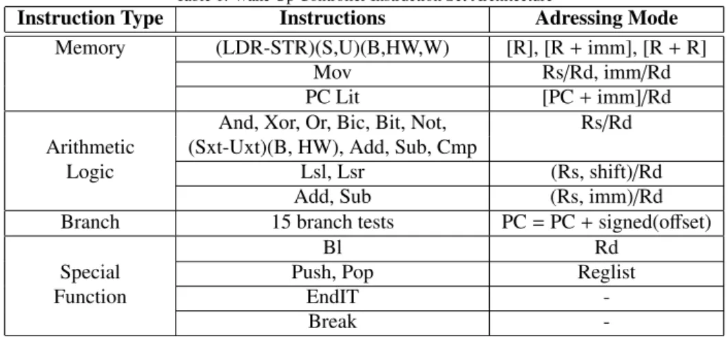
The WUC implements a 16-bit Instruction Set Architecture (ISA) based on load/store RISC instructions. It has to remain simpler than a classical CPU ISA and architecture as the objective is to consume few energy for wake-up and current tasks. The ISA has thus been specified to
Table 1: Wake Up Controller Instruction Set Architecture
Instruction Type Instructions Adressing Mode Memory (LDR-STR)(S,U)(B,HW,W) [R], [R+ imm], [R + R]
Mov Rs/Rd, imm/Rd PC Lit [PC+ imm]/Rd And, Xor, Or, Bic, Bit, Not, Rs/Rd Arithmetic (Sxt-Uxt)(B, HW), Add, Sub, Cmp
Logic Lsl, Lsr (Rs, shift)/Rd Add, Sub (Rs, imm)/Rd Branch 15 branch tests PC= PC + signed(offset)
Bl Rd
Special Push, Pop Reglist
Function EndIT
-Break
-be compact and easy to program by developing a compiler. Therefore C language can -be used to program Interrupt Service Routine executed by the WUC. Each instruction is 16-bit wide. It has 16 32-bit general purpose registers including the Stack Pointer (SP), the Link Register (LR) and the Program Counter (PC). The address is on 16 bit which is sufficient for the small memory used by the WUC and low power peripherals. It also significantly reduces the total power consumption.
The WUC instruction set architecture has been reduced to fit our needs, stay compact and adapt to multiple peripherals. Load-store instructions is implemented because the WUC is in charge of the WSN microcontroller current tasks. In other words, it has to manage data transfer from sensors or radio to memory, and vice versa. Therefore, the load-store instruction is manda-tory and can handle 8, 16 and 32 bit data to fit a maximum of peripheral modules. Arithmetic instructions are also implemented since the WUC manages peripheral configuration which needs logic instructions for masking operations. And, it also has to perform some calculation on the data or the address. The branch instruction was required to go through the event-triggered code, which relies on a state machine. Branch instruction is then used to jump from one state to an-other. Finally for easy programming and reduced number of instructions, special instructions for function call and context save-restore have been implemented.
Table 1 resumes our proposed WUC instructions. There are 4 types of instructions: Memory, Arithmetic/Logic, Branch and Special/Function instructions. Memory instructions can manage byte, half-word and word data in signed or unsigned type. Arithmetic and logic instructions handle 32 bit data and there are 15 instructions to test branches. Some instructions have been implemented for function calls (Branch with Link) and context save-restore (push/pop) with a single 16 bit instruction. It is important to notify that the proposed WUC executes only Interrupt Service Routine (ISR). This is the reason why an instruction is necessary to indicate the end of interruption (EndIT). A special instruction Break can set breakpoints in memory providing an on-chip debugging during code execution.
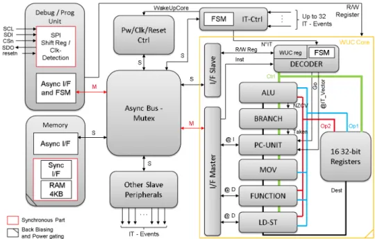
5.2. Wake Up Controller Core Microarchitecture
The microarchitecture of the Always Responsive part is presented in Figure 10. From the pre-viously presented instruction set architecture, five execution units have been created. Arithmetic
and Logic Unit (ALU) for arithmetic and logic operations updating status bit NZCV (Negative, Zero, Carry, Overflow bit) that are used by BRANCH unit to test branches. A load-store unit (LD-ST) and MOV unit are used for Memory instructions, and FUNCTION unit for Bl, Push and Pop instructions. There are three fast bus for operand 1, 2 and result (Op1, Op2 and Dest) between register file and execution units. The DECODER inputs multiple control signals to configure execution unit and datapath at each instruction. The WUC presents a Von Neumann architecture with only 4KB memory for program, data and interrupt vector. The Memory and all slaves/masters of the Always Responsive part are linked by an asynchronous bus. There are two masters, the WUC Core and the Debug Unit that can program, read-write on all address space and on the general purpose registers as well as the operate stop, run and step commands to the WUC while the code is executing. IT-Ctrl manages all events from all peripherals and sends to the DE-CODER the number of the priority interrupt. Interruptions are sorted by interruption numbers with the highest priority on interrupt number 0 and interrupt with the weakest priority on inter-rupt number 31. In a typical scenario, if the system is in off mode, only IT-Ctrl, Pw/Clk/Reset Ctrl and some peripherals are powered on. And when an event occurs from a peripheral, IT-Ctrl gets it, sends a signal to Pw/Clk/Reset Ctrl to wake up the WUC Core (if powered off), and then sends to the DECODER the rising interrupt number. The DECODER calculates the address of the interrupt vector with a configurable offset, then sends this address to PC Unit in order to fetch the address of interrupt service routine and then fetches the first instruction of the ISR. When an EndIT instruction is decoded, IT-Ctrl checks if another event is pending or not. It sends the new number of interrupt to DECODER or sends to Pw/Clk/Reset Ctrl a sleep signal to power gate the WUC Core or not depending on the users configuration. During execution, an instruction is executed to completion before fetching next instruction. This is done by blocking the control signals from DECODER to the execution unit. In practice, with asynchronous logic, handshake channels are acknowledged once the instruction is completed.
5.3. Memory
The WUC has one 4KB memory bank of 32-bit lines. This memory has been specified to be the smallest considering its static and dynamic power consumption. Only 4KB are required for data of maximum 32-bit width, program and interrupt vector. Code size in different ISR is very small so this memory size is sufficient for a complete WUC application. In terms of power manage-ment, the memory has its own power domain and can take advantage of the wide operating volt-age range of the UTBB FDSOI technology. This memory has an optimal functional point at 0.5V and can have retention at 0.3V. As such, during the retention phase, supply voltage is lowered to 0.3V and during activity it can be raised to 0.5V and up to 0.7V depending on applicative perfor-mances. At architectural level, only one port is used for instructions and data read-write opera-tions to reduce memory and WUC complexity (Von Neumann Architecture). Moreover, a mask port is used to select bytes to write on a 32 bit line. The memorys asynchronous/synchronous interface is presented on Figure 11. For mixed asynchronous/synchronous design, Tiempo® interfaces are used to convert asynchronous handshake channels to synchronous data. In this interface, write request and read request that cross delay chains create the acknowledgement of the input/output channels. This indicates to the asynchronous part the end of operation. Different timing delay chains can be used for read/write operations. The architecture of the asymmetric delay chain used in this asynchronous circuit is presented in Figure 12.
The delay chain is used to prevent new requests from being taken into account while the current request is not completed. This is done with a Muller tree and inverters at each buffer
Figure 10: Always Responsive part microarchitecture with Wake Up Controller Core architecture
Figure 11: Mixed asynchronous/synchronous design for memory interface. M is a Muller Cell [17]
output. Moreover, AND gates are used with each output buffer and delay chain input to quickly lower the acknowledge signal when request goes down. Consequently, when a request rises, the acknowledgement signal is generated after n bu f f er × D ns, and when the request signal goes down, the acknowledgement signal goes down after D ns. With this architecture, read-write timing operations are respected with minimal overhead between two memory accesses.
Figure 12: Asymmetric delay chain for asynchronous circuit
5.4. System Supply
From Section 3, we can assume that for an energy efficient Always Responsive part, the best UTBB FDSOI implementation should use RVT cells in order to activate the reverse back bi-asing possibilities and greatly reduce leakage current during long retention phases (Figure 3). Moreover, it is not necessary to achieve high performance on this part, and so RVT is the best compromise between power and frequency. Thanks to the wide operating voltage range of UTBB FDSOI with back biasing possibilities and asynchronous design, the WUC Core can have its own power domain and operate at MEP (0.2V) to reach the optimal power efficiency. The WUC Core power supply voltage can be regulated depending on the required performances, from 0.2V up to 0.7V. This flexibility allows the WUC Core to be powered at 0.2V during retention phase with maximum RBB to reduce leakage current and while in activity, it can be supplied with-out RBB at MEP or higher power supply voltage following users requirement. Taking this into considerations, the system supply for the Always Responsive part has been determined (Figure 13). The Always Responsive part is divided into three voltage domains (VD CORE, VD AON, VD MEM) and resulting into four power domains (PD CORE, PD MEM, PD SYSTEM and PD PERIPHERALS). In VD AON, there is an always-on power domain PD SYSTEM and a power gated power domain PD PERIPHERALS. We chose to separate the WUC Core and Mem-ory in two power domains to fit different power management strategies like power gating and back biasing of UTBB FDSOI 28 nm technology in multiple scenarios. The central module for controlling the fine grain power gating, clock gating and back biasing is the Pw/Clk/Reset Controller (Figure 13). Its able to automatically power gate the core if no ISR is executing, or apply an automatic back biasing on memory and WUC Core when executing code. For very simple applications for which only a timer is needed to wake up the entire system, an RTC is implemented in PD SYSTEM and PD PERIPHERALS which can be power gated during re-tention phase. The next section presents firsts results in term of area and leakage power with ongoing Always Responsive part modules development and implementation flow of a mixed asynchronous/synchronous circuit.
Figure 13: Always Responsive part power domains and clock distribution
6. Implementation Flow and First Results 6.1. Implementation Flow
The Asynchronous modules are coded in SystemVerilog using Tiempo® tools [14] [15] [16] for channels assertion, read-write between a transmitter and a receiver, and for registers and op-erators assertion. We use a mixed implementation flow with a synchronous top that instantiates asynchronous macros. The Asynchronous part is synthesized using the Asynchronous Circuit Compiler (ACC) from Tiempo®, and the synchronous parts are synthesized with Design Com-piler from Synopsys tools. The test-benches are simulated at each step of the implementation flow (functional, post-synthesis and post back-end). For synthesis, the UTBB FDSOI 28 nm technology is used. Some asynchronous and standard synchronous cells are provided in the library for the full system synthesis.
6.2. Area Results
The results presented hereafter are post-synthesis figures in UTBB FDSOI 28 nm. These results are related to a circuit containing the WUC Core, the Asynchronous Bus (2 masters and 7 slaves), the 4KB Memory and the IT-Ctrl (32 ITs). Figure 14a depicts WUC Core, Asynchronous Bus, IT-Ctrl and Memory area and Figure 14b presents the WUCs internal modules size. As can be seen, the WUC Core represents 51% of the total area. However, WUC Core can be power gated or configured in its less power consuming mode (0.2V with maximum RBB) during long retention phases to reduce the leakage power. Moreover current IT-Ctrl can manage 32 ITs, but this can be reduced to 16 or 8 general ITs with the help of a module routing each event
from all peripherals to an IT vector with a configuration register. With this technique, the IT-Ctrl area is reduced by half. Leakage power consumption are presented on Figure 14c. This leakage power consumption is measured with post synthesis simulation at 0.3V Vdd without back biasing. It results, for retention, in a power consumption of about 1µW. By applying reverse back biasing, we can obtained a hundred of nWs while remaining in a functional mode. Design and architectural optimizations to reduce even more power consumption and area will be discussed in the conclusion of the paper.
Figure 14: Wake Up Controller area and leakage power consumption at 0.3V (during retention phase) results for 32 bits datapath implementation
7. Conclusion and Future Work
For the past ten years, IoT devices have emerged with constant constraints on leakage and integration. Today’s wireless sensor nodes are proposed in old technology nodes for leakage and cost reasons. In this paper, we have discussed UTBB FDSOI 28 nm suitability and new micro-controller architectural solutions for ultra low power IoT applications. FDSOI back biasing and performances at low voltage make this technology extremely suitable for the flexible needs of the IoT applications. Moreover, in this paper, flexibility is provided by partitioning the micro-controller into an Always Responsive part and an On Demand part. In the Always Responsive part, an asynchronous Wake Up Controller is implemented for fast wake up and robustness to voltage variations. The WUC manages current tasks of the WSN microcontroller while the main processor of the On Demand part is in charge of the application part and the node maintenance.
We have efficiently applied UTBB FDSOI 28 nm on this microcontroller and opened the way for new applications requiring more speed during operation while maintaining low leakage during idle phases.
Furhtermore, to reduce the total power consumption of this microcontroller, we are proposing some architectural improvements as future works. We can first simplify the WUC Core and Bus by decreasing the datapath width to 16 bits. In the WUC Core, the units that will benefit from a datapath width reduction are the Register File, the ALU Unit, the FUNCTION and the LD-ST Unit (Figure 14b). We can expect an area and power reduction by at least a factor of two for these units. We will thus need to reconsider the Instruction Set Architecture since all load/store 32 bits data instructions will be supressed as well as the 16 bits sign/unsigned extend instructions. Therefore, we are currently investigating new interesting instructions to efficiently replace them. In addition, and in order to reduce the dynamic power consumption, a cache line for instruction will be integrated to avoid useless consecutive instruction fetch in the 32 bits memory line.
References
[1] Y. Lee, Y. Kim, D. Yoon, D. Blaauw, D. Sylvester, Circuit and system design guidelines for ultra-low power sensor nodes, in: Design Automation Conference (DAC), 2012 49th ACM/EDAC/IEEE, 2012, pp. 1037–1042.
[2] D. Bol, J. De Vos, C. Hocquet, F. Botman, F. Durvaux, S. Boyd, D. Flandre, J. Legat, Sleepwalker: A 25-mhz 0.4-v sub- mm27 − µW/MHz microcontroller in 65-nm lp/gp cmos for low-carbon wireless sensor nodes, Solid-State
Circuits, IEEE Journal of 48 (1) (2013) 20–32. doi:10.1109/JSSC.2012.2218067.
[3] R. Aitken, V. Chandra, J. Myers, B. Sandhu, L. Shifren, G. Yeric, Device and technology implications of the internet of things, in: VLSI Technology (VLSI-Technology): Digest of Technical Papers, 2014 Symposium on, 2014, pp. 1–4. doi:10.1109/VLSIT.2014.6894339.
[4] E. Beigne, A. Valentian, I. Miro-Panades, R. Wilson, P. Flatresse, F. Abouzeid, T. Benoist, C. Bernard, S. Bernard, O. Billoint, S. Clerc, B. Giraud, A. Grover, J. Le Coz, J.-P. Noel, O. Thomas, Y. Thonnart, A 460 mhz at 397 mv, 2.6 ghz at 1.3 v, 32 bits vliw dsp embedding f max tracking, Solid-State Circuits, IEEE Journal of 50 (1) (2015) 125–136. doi:10.1109/JSSC.2014.2369503.
[5] G. Kim, Y. Lee, Z. Foo, P. Pannuto, Y.-S. Kuo, B. Kempke, M. Ghaed, S. Bang, I. Lee, Y. Kim, S. Jeong, P. Dutta, D. Sylvester, D. Blaauw, A millimeter-scale wireless imaging system with continuous motion detec-tion and energy harvesting, in: VLSI Circuits Digest of Technical Papers, 2014 Symposium on, 2014, pp. 1–2. doi:10.1109/VLSIC.2014.6858425.
[6] J. Myers, A. Savanth, D. Howard, R. Gaddh, P. Prabhat, D. Flynn, 8.1 an 80nw retention 11.7pj/cycle active subthreshold arm cortex-m0+; subsystem in 65nm cmos for wsn applications, in: Solid- State Circuits Conference - (ISSCC), 2015 IEEE International, 2015, pp. 1–3. doi:10.1109/ISSCC.2015.7062967.
[7] STMicroelectronics, Datasheet STM32L063C8 STM32L063R8, rev. 2 (4 2014). [8] TI, CC2650 SimpleLink Multistandard Wireless MCU, rev. 2 (10 2015).
[9] J.-C. Barbe, L. Lucci, A. Siligaris, P. Vincent, O. Faynot, 4-port rf performance assessment and compact modeling of utbb-fdsoi transistors, in: Radio Frequency Integrated Circuits Symposium (RFIC), 2015 IEEE, 2015, pp. 355– 358. doi:10.1109/RFIC.2015.7337778.
[10] E. Beigne, A. Valentian, B. Giraud, O. Thomas, T. Benoist, Y. Thonnart, S. Bernard, G. Moritz, O. Billoint, Y. Maneglia, P. Flatresse, J. Noel, F. Abouzeid, B. Pelloux-Prayer, A. Grover, S. Clerc, P. Roche, J. Le Coz, S. Engels, R. Wilson, Ultra-wide voltage range designs in fully-depleted silicon-on-insulator fets, in: Design, Au-tomation Test in Europe Conference Exhibition (DATE), 2013, 2013, pp. 613–618. doi:10.7873/DATE.2013.135. [11] E. Zianbetov, E. Beigne, G. Di Pendina, Non-volatility for ultra-low power asynchronous circuits in hybrid
cmos/magnetic technology, in: Asynchronous Circuits and Systems (ASYNC), 2015 21st IEEE International Sym-posium on, 2015, pp. 139–146. doi:10.1109/ASYNC.2015.27.
[12] M. Hayashikoshi, Y. Sato, H. Ueki, H. Kawai, T. Shimizu, Normally-off mcu architecture for low-power sen-sor node, in: Design Automation Conference (ASP-DAC), 2014 19th Asia and South Pacific, 2014, pp. 12–16. doi:10.1109/ASPDAC.2014.6742852.
[13] F. Berthier, E. Beigne, P. Vivet, O. Sentieys, Power gain estimation of an event-driven wake-up controller dedicated to wsn’s microcontroller, in: New Circuits and Systems Conference (NEWCAS), 2015 IEEE 13th International, 2015, pp. 1–4. doi:10.1109/NEWCAS.2015.7182064.
[14] Tiempo, Tiempo asynchronous Technology introduction, rev. 1.1 (6 2009). [15] Tiempo, Introduction to SystemVerilog Asynchronous Modeling, rev. 2.0 (3 2011).
[16] Tiempo, Introduction to Testing Tiempo Asynchronous Circuits, rev. 1.0 (6 2010).
[17] A. Martin, M. Nystrom, Asynchronous techniques for system-on-chip design, Proceedings of the IEEE 94 (6) (2006) 1089–1120. doi:10.1109/JPROC.2006.875789.