HAL Id: tel-01279190
https://tel.archives-ouvertes.fr/tel-01279190
Submitted on 25 Feb 2016HAL is a multi-disciplinary open access archive for the deposit and dissemination of sci-entific research documents, whether they are pub-lished or not. The documents may come from teaching and research institutions in France or abroad, or from public or private research centers.
L’archive ouverte pluridisciplinaire HAL, est destinée au dépôt et à la diffusion de documents scientifiques de niveau recherche, publiés ou non, émanant des établissements d’enseignement et de recherche français ou étrangers, des laboratoires publics ou privés.
Flexible devices for energy harvesting based on printed
organic piezoelectric P(VDF-TrFE) materials
Elena Gusarova
To cite this version:
Elena Gusarova. Flexible devices for energy harvesting based on printed organic piezoelectric P(VDF-TrFE) materials. Electric power. Université Grenoble Alpes, 2015. English. �NNT : 2015GREAT139�. �tel-01279190�
THÈSE
Pour obtenir le grade de
DOCTEUR DE LA COMMUNAUTÉ UNIVERSITÉ
GRENOBLE ALPES
Spécialité : Nanoélectronique et nanotechnologie Arrêté ministériel : 7 août 2006
Présentée par
Elena Gusarova
Thèse dirigée par Bernard Viala
préparée au sein du Laboratoire CEA-Leti
dans l'École Doctorale d'Electronique, Electrotechnique, Automatique, Traitement du Signal (EEATS)
Dispositifs souples pour la
récupération d’énergie à base de
matériaux organiques piézoélectriques
P(VDF-
TrFE) imprimés
Thèse soutenue publiquement le 16 décembre 2015, Devant le jury composé de:
Dr. Paul Muralt
Professeur, EPFL, Rapporteur et président
Dr. Philippe Pernod
Professeur, Ecole Centrale de Lille, Rapporteur
Dr. Ian Cayrefourcq
Docteur Ingénieur, Directeur des technologies Emergentes, Arkema-France, Membre
Dr. Bernard Viala
Ingénieur de Recherche, HDR, CEA-Leti, Directeur de thèse
Dr. Orphée Cugat
Directeur de Recherche, CNRS, G2ELab, Co-directeur de thèse
Dr. Leticia Gimeno
Maitre de conférences,UJF/UGA, G2ELab, Encadrant
Dr. Romain Gwoziecki
Résumé
δe but de cette thèse était d’étudier des solutions innovantes pour la récupération d’énergie pour pouvoir alimenter de manière autonome les futurs capteurs et nœuds communicants sans fil de l’Internet des Objets (IoT pour Internet of Things). δe travail s’est focalisé sur des matériaux piézoélectriques souples et sur une approche composite et multiphysique. δ’objectif est de récupérer de l’énergie à partir de déformations directes ou induites provenant de sources à la fois mécaniques et thermiques et en particulier de sources négligées jusqu’alors (lentes et de faibles intensités). δ’idée maitresse est l’hybridation de plusieurs matériaux fonctionnels avec un cœur du système constitué par des microgénérateurs piézoélectriques (et pyroélectriques) imprimés nécessaires à la génération de charges électriques. δ’originalité de ce travail est d’avoir réalisé un système de récupération d’énergie entièrement flexible, au format d’une carte de crédit et compatible avec de plus grandes dimensions, en utilisant des copolymères piézoélectriques de P(VDF-TrFE) sous forme d’encres. Ce matériau est flexible et particulièrement résistant, ce qui le rend attractif pour des applications mettant en jeu formes complexes, notamment, courbes. Un autre avantage du copolymère de P(VDF-TrFE) est qu’il ne nécessite pas de pré-déformation mécanique comme pour le polymère PVDF et il commence à être aujourd’hui disponible sous forme d’encres pour l’électronique imprimée, ce qui simplifiera et réduira les coûts de fabrication à termes.
En premier, nous décrivons le procédé de fabrication par sérigraphie des microgénérateurs en P(VDF-TrFE), suivi par les caractérisations ferroélectriques puis piézoélectriques des dispositifs. A cet effet, nous avons développé des techniques de mesures originales en circuit ouvert qui ont été testées et validées au préalable avec des échantillons de PVDF commercial. δa dernière étape a été de réaliser un prototype de récupération d’énergie thermique flexible de faible encombrement (sans radiateur). Cela a été réalisé en hybridant les microgénérateurs précédemment fabriqués avec des feuilles d’alliages à mémoire de forme thermique à base de NiTi, qui est un matériau sensible à un seuil de température donnée.
δes résultats phares de cette étude sont : 1) le dépôt multicouches de P(VDF-TrFE) combiné au dépôt d’une électrode souple en PEDOT:PSS, β) l’établissement des caractéristiques ferroélectriques et piézoélectriques en fonction de l’épaisseur de P(VDF-TrFE) et enfin γ) la détermination d’un coefficient g supérieur à la normale avec
tensions utiles de l’ordre de 10 V avec ici une densité d’énergie de proche de 500 μJ/cm3
, ces valeurs étant limitées aux conditions de test utilisées.
Nous concluons ce travail sur une preuve de concept fonctionnelle de récupérateur d’énergie thermique flexible apte à détecter ou utiliser des variations lentes et faibles de température à partir de sources élémentaires, produisant pour l’instant γ7 V (correspondant à 95 µJ) à 65 ºC, et qui à termes pourront être l’air ambiant (chaud ou froid) ou la chaleur de la peau.
Abstract
This work aims to study innovative solutions for energy harvesting applicable to autonomous wireless sensors for IoT (Internet of Things). It is focused on flexible piezoelectric composite materials and a multi-physical approach. The objective is to harvest energy via strain-induced phenomena from both mechanical and thermal sources, and particularly sources neglected so far (slow and low). The main idea is the hybridization of different functional materials with the core of the system being screen printed piezo/pyro-electric microgenerators, mandatory to generate piezo/pyro-electrical charges. The originality of this work is to realize large area flexible energy harvesting systems by using ink-based piezoelectric copolymers of polyvinylidene fluoride P(VDF-TrFE). This material is very flexible and durable which makes it attractive for applications in systems with complex shapes. Another benefit of P(VDF-TrFE) is that it does not need to be pre-stretched as PVDF and it is now available in inks for printable electronics which can simplify and reduce the price of the fabrication process.
We first describe the fabrication process of the screen printed P(VDF-TrFE) microgenerators, followed by ferroelectric and piezoelectric characterizations. For this purpose we have developed optimized methods in open-circuit conditions adapted for flexible systems tested and validated on commercial bulk PVDF. The last step was to realize a low profile thermal flexible energy harvester prototype (no radiator). It was done by hybridization of the fabricated microgenerators and foils of shape memory NiTi-based alloy, which is a functional material sensitive to a given temperature threshold.
The key outcomes of this work are: 1) the successful deposition of multilayers of P(VDF-TrFE) and organic PEDOT:PSS electrode, 2) dielectric, ferroelectric and direct piezoelectric constants reported as a function of film thickness, and 3) the g31 direct voltage
coefficient, measured for the first time, and showing the record value of 0.15 V·m/N. Also, we have demonstrated that in open-circuit conditions, the microgenerators can produce a useful strain-induced voltage of 10 V with an energy density close to 500 μJ/cm3, these values being limited by the experimental set-up.
The concept of thermal energy harvesting composite based on thin film screen printed P(VDF-TrFE) microgenerators was realized and demonstrated to be effective. We conclude with a functional prototype of flexible energy harvester, able to detect non-continuous slow
Acknowledgements
I would like first to thank my wonderful supervisor team: Bernard Viala, Orphée Cugat and Leticia Gimeno. Thank you for guiding and encouraging me, showing opportunities and giving constructive critics.
There have been many people who helped me and worked side by side during these years. I would like to thank each and every one of them. I would especially like to thank Aurélia Plihon, who taught me a lot, Gor Lebedev and Dmitry Zakharov, whose example inspired me and put me on this road. And, of course, the girls from my office: Hélène Takacs, Jennifer Guillaume and Raissa Shema who helped me to settle in a new country and learn a new language.
Very big thanks must also go to my good friends Pasha Shpak and Ivan Voznyuk, which I met during this work and who shared the working life, joy and supported me at the most difficult times.
Finally, I would like to dedicate this work to my beloved husband Boris Gusarov, who is the Atlas which holds my World on his shoulders.
Contents
List of figures ... xiii
List of tables ... xix
Chapter 1. Introduction and motivations ... 1
1.1 Flexible electronics ... 2
1.1.1 Printed electronics: usual techniques ... 2
1.1.2 Printed electronics: the emblematic example of RFID ... 6
1.1.3 Printed electronics: flexible and transparent electrodes ... 8
1.2 Energy harvesting: towards flexibility ... 9
1.2.1 Introduction to piezoelectricity and pyroelectricity ... 13
1.2.2 Piezoelectric polymers: state of the art ... 17
1.2.3 Piezoelectric polymers: nanostructuration ... 20
1.2.4 Piezoelectric polymers: composites with shape memory alloy ... 23
1.3 Summary of the targets of this work ... 24
Chapter 2. Fabrication process for flexible piezoelectric microgenerators ... 27
2.1 Materials and methods ... 27
2.1.1 Sample fabrication: overall process flow ... 27
2.1.2 Sample fabrication: multilayer deposition of P(VDF-TrFE) ... 33
2.1.3 Sample fabrication: top electrode materials ... 36
2.2 Design and test structures ... 37
2.2.1 Design-1: single capacitor ... 38
2.2.2 Design-2: parallel connected capacitor network ... 39
2.2.3 Design-3: interdigital electrodes ... 40
2.4 Summary of the fabrication ... 47
Chapter 3. Ferroelectric properties ... 49
3.1 State of the art ... 49
3.1.1 Poling methods for polymers ... 49
3.1.2 Ferroelectric properties of P(VDF-TrFE) ... 52
3.2 Materials and methods ... 52
3.2.1 Poling conditions ... 53
3.2.2 C-V measurement ... 53
3.2.3 P-E measurement ... 54
3.3 Results and discussion ... 54
3.3.1 Capacitances of P(VDF-TrFE) ... 55
3.3.2 Hysteresis loops of P(VDF-TrFE) ... 56
3.3.3 Aging with PEDOT:PSS ... 58
3.3.4 Effects of top electrode materials ... 59
3.4 Exploratory: heterostructures ... 61
3.5 Summary of electrical results ... 66
3.6 Conclusions ... 68
Chapter 4. Piezoelectric properties ... 69
4.1 Materials and methods ... 69
4.1.1 Direct piezoelectric voltage measurements ... 70
4.1.2 Strain application ... 72
4.1.3 Sample preparation ... 74
4.2 Results and discussion ... 75
4.2.1 Piezoelectric voltage ... 75
4.2.2 Piezoelectric coefficient (g31) ... 78
4.2.3 Piezoelectric energy density ... 79
Chapter 5. Prospective works ... 85
5.1 Flexible composite thermal harvester ... 85
5.1.1 Principle (multi-physical) ... 85
5.1.2 SMA (short reminder) ... 86
5.1.3 Materials and methods ... 88
5.1.4 Electrical results ... 91
5.1.5 IoT Energy issues ... 93
5.2 Building blocks for a thermal IoT sensor ... 97
5.3 Further energy increase: nanostructuration ... 100
5.4 Conclusions ... 104
General conclusions ... 105
δist of figures
Figure 1.1. Schematic representation of the screen printing process. ... 3
Figure 1.2. Schematic representation of the gravure printing process [7]. ... 4
Figure 1.3. Schematic representation of the inkjet printing process [7]... 5
Figure 1.4. RFID system [18]. ... 7
Figure 1.5. RFID tag [18]. ... 7
Figure 1.6. The backbone structure of PEDOT. ... 8
Figure 1.7. The backbone structure of PEDOT:PSS. ... 9
Figure 1.8. Power from body-driven sources; total power for each action is included in parentheses [27]. ... 10
Figure 1.9. System of raindrop energy harvesting from [28]. ... 10
Figure 1.10. Strain generation by bending of all-polymer piezoelectric energy harvesting device [29]. ... 11
Figure 1.11. Scheme of the experimental set-up used to investigate the direct piezoelectric response of the P(VDF-TrFE) samples [30]. ... 12
Figure 1.12. (a) Schematic illustration of the flexible nanogenerator, (b) photo images of the nanogenerator at various location on human body, showing good compatibility of the device with various parts of body [31]. ... 12
Figure 1.13. Stretch and release cycles scheme of mechanical loading equipment. ... 13
Figure 1.14. Axis definition of piezo elements. ... 14
Figure 1.15. Schematic presentation of the transformation in PVDF from α to -phase. [39]. 17 Figure 1.16. Theoretical absolute voltage output as function of applied strain for different piezoelectric materials for 1 µm thickness. ... 20
Figure 1.17. Schematic drawing of the nanoimprint process of PVDF-TrFE polymer. [49]. . 21
Figure 1.18. Nanoimprint process steps. ... 22
Figure 1.19. Property change vs. temperature for a martensitic transformation occurring in a shape memory alloy. The parent phase (austenite) is represented by the square lattice, which upon martensitic transformation is distorted into the rhombic martensite phase [59]. ... 24
Figure 2.2. The overall process flow of sample fabrication. ... 28
Figure β.γ. Cracks on the β.6 µm screen printed P(VDF-TrFE) samples without preliminary annealing. ... 29
Figure 2.4. Screen printing deposition process with Ekra. The screen and the squeegee are visible. ... 32
Figure 2.5. Plate capacitor (MIM-structure). ... 32
Figure 2.6. Typical profile of two deposited layers of P(VDF-TrFE). ... 34
Figure 2.7. Microtomy cross-section SEM image of a bilayer of P(VDF-TrFE) after annealing. The whole structure of the microgenerator is also shown. ... 35
Figure 2.8. Cross-section SEM image of microgenerator with Ag top electrode. ... 36
Figure 2.9. Cross-section SEM image of microgenerator with Ag top electrode (higher zoom). A flake of Ag ink is penetrating into P(VDF-TrFE). ... 37
Figure 2.10. Design-1: single capacitor MIM structure. ... 38
Figure 2.11. Screen printed P(VDF-TrFE) single MIM capacitor test structures for material study. Only Au at the bottom electrode can be seen on the picture as P(VDF-TrFE) and PEDOT:PSS are transparent. ... 39
Figure 2.12. Design-2 in CleWin 5 software. ... 39
Figure 2.13. Network of 45 parallel connected capacitors of P(VDF-TrFE) in a credit card format. ... 40
Figure 2.14. P1 type MFC actuator. ... 41
Figure 2.15. Design of IDE with corresponding geometrical parameters (not to scale). ... 41
Figure 2.16. Fabricated IDE structures on PEN substrate. ... 42
Figure 2.17. Visualization of theoretical electric field in β.6 µm thick P(VDF-TrFE) with applied 300 V to 5/5 µm IDE design. ... 42
Figure 2.18. Schematic of the multilayer heterostructure configurations of screen printed P(VDF-TrFE) and P(VDF-TrFE-CTFE). ... 44
Figure 2.19 Cross-section SEM image of the 2-step deposited P(VDF-TrFE) and 1-step deposited P(VDF-TrFE-CTFE). ... 45
Figure 3.1. Simplified scheme schematic diagram of electrode (thermal) poling of PVDF. ... 50
Figure 3.2. Schematic diagram of corona poling of polymers [94]. ... 51
Figure 3.3. Schematic diagram of electron beam poling. The electrons penetrate into the polymer and form a space-charge layer [95]. ... 51
Figure 3.4. Pictures of the aixACCT TF Analyzer 2000E with FE-Module, and close up of the probe station. ... 53
Figure 3.5. Capacitance thickness-dependence of screen printed P(VDF-TrFE) single capacitors. ... 55 Figure 3.6. Leakage current density of screen printed P(VDF-TrFE) capacitors with
PEDOT:PSS top electrode as function of thickness, measured at 1 kHz. ... 56 Figure 3.7. Typical r-E -E curves butterfly loop at 0.1 Hz ou 1 kHz ? of β.6 µm
thick screen printed P(VDF-TrFE). Adjust the size ! ... 57 Figure 3.9. Typical frequency dependence of hysteresis loop of 2.6 µm thick screen printed
P(VDF-TrFE). ... 58 Figure 3.10. Time-dependence of the capacitance of PEDOT:PSS based capacitors. ... 59 Figure 3.11. Frequency-dependences of permittivity and loss tangent of 2.6 µm thick screen
printed P(VDF-TrFE) capacitors with Ag and PEDOT:PSS top electrodes. ... 60 Figures 3.12. Leakage current density at 1 kHz vs. voltage of 2.6 µm thick screen printed
P(VDF-TrFE) capacitors with Ag (a) and PEDOT:PSS (b) top electrodes. Note the different scales. ... 61 Figure 3.13. Typical r-E -E curves butterfly loop at 1 kHz of 2.2 µm thick screen
printed P(VDF-TrFE-CTFE). ... 62 Figure γ.15. Frequency dependence of hysteresis loop of β.β µm screen printed P(VDF-TrFE-CTFE). ... 63 Figure 3.16. Leakage current densities at 0.1 Hz and 100 Hz vs. electric field of 2.2 µm screen
printed P(VDF-TrFE-CTFE). ... 64 Figure 3.17. P-E hysteresis loop of screen printed heterostructure of P(VDF-TrFE) and
P(VDF-TrFE-CTFE) for different frequencies (sample multi-P-1). ... 65 Figure 3.18. Leakage current densities of screen printed heterostructure of P(VDF-TrFE) and
P(VDF-TrFE-CTFE) for different frequencies (sample multi-P-1). ... 65 Figure 3.19. Electrical schematic representation of multilayer (sample multi-P-3) with
material capacitors connected in series including interface capacitance (in red). . 67 Figure 4.1. Schematic presentation of the switch measurement circuits with oscilloscope or
non-contacting electrostatic voltmeter. ... 70 Figure 4.2. (a) oscilloscope Agilent Technologies DSO1014A, (b) non-contacting electrostatic
voltmeter TREK 370. ... 70 Figure 4.3. Examples of piezoelectric discharge of commercial grade PVDF using
oscilloscope with switch, electrostatic voltmeter with switch, and comparison with conventional measurement (oscilloscope only). ... 71
Figure 4.5. Four-point bending system: (a) experimental set-up, (b) schematic representation. ... 73 Figure 4.6. Single screen printed capacitor structures mounted on Plexiglas for four-point
bending experiment. ... 74 Figure 4.7. Screen printed parallel connected capacitor structures used for tube bending
experiment (no additional substrate). ... 75 Figure 4.8. Piezoelectric output voltage of commercial grade PVDF (40 µm) from Piezotech
based on four-point bending and tube bending in open-circuit condition. Solid line is theoretical from data sheet characteristics. Should be vs stress and not strain ! 76 Figure 4.9. Piezoelectric output voltage of the screen printed P(VDF-TrFE) single capacitor,
obtained by four-point bending in open-circuit condition for various thicknesses. ... 77 Figure 4.10. Piezoelectric voltage as a function of applied stress for the screen printed
P(VDF-TrFE) parallel connected microgenerators with β.6 µm thickness. ... 78 Figure 4.11. Energy density values under applied strain for screen printed P(VDF-TrFE)
single microgenerators with various thicknesses. ... 80 Figure 4.12. Energy as a function of strain for the screen printed P(VDF-TrFE) parallel
connected microgenerators. ... 80 Figure 4.13. Pyroelectric voltage as a function of temperature for the screen printed P(VDF-TrFE) parallel connected microgenerators of β.6 µm thickness. ... 81 Figure 5.1. Schematic illustrating different types of coupling present in the composite. ... 86 Figure 5.2. Temperature-induced phase transformation of an SMA without mechanical
loading [108]. ... 86 Figure 5.3. Temperature-induced phase transformation with applied load [108]. ... 87 Figure 5.4. Photo of the flexible thermal composite (credit card format). Screen printed
P(VDF-TrFE) microgenerators are visible on top, and NiTi sheet is visible by transparency. ... 89 Figure 5.5. Flexible thermal composite operation scheme. Composite is pre-strained by tube
bending at room temperature, then heated and recovered its initial state. ... 90 Figure 5.6. Schematic of SMA + piezoelectric composite functioning. ... 91 Figure 5.7. Piezoelectric, pyroelectric and combined voltages vs. time of the flexible thermal
composite. Piezoelectric measurement performed at room temperature with 0.56% strain, pyroelectric measurement performed at 65 ºC unstrained and crossed piezo/pyro measurement performed at 65 ºC pre-strained (equivalent 0.56%
Figure 5.8. Piezoelectric, pyroelectric and combined voltages vs. strain of the flexible thermal composite. Piezoelectric measurement performed at room temperature with 0.56% strain, pyroelectric measurement performed at 65 ºC unstrained and crossed piezo/pyro measurement performed at 65 ºC pre-strained (equivalent 0.56%
strain). ... 93
Figure 5.9. Powers consumed by CMOS electronic devices [58]. ... 94
Figure 5.10. ZigBee® δight smart mesh schematic [117] ... 95
Figure 5.11. Summary of wireless technology parameters [116]... 96
Figure 5.12. Complete conversion power management circuit. The input P(VDF-TrFE) composite is on the left side, and the output is on the right, supplying RF transmitter with antenna. ... 97
Figure 5.13. Complete conversion switch power management circuit with diode bridge (optional) and buck converter [121]. ... 98
Figure 5.14. Electric diagram of the TPS62122 buck converter. ... 99
Figure 5.15. Emission (left) and reception (right) wireless cards (CEA Showroom). ... 99
Figure 5.16. Examples of possible self-powered applications from Thinfilm [122]. ... 100
Figure 5.17. Obducat Nano Imprint Lithography EITRE machine ... 101
Figure 5.18. AFM (left) and SEM (right) images of nanoimprinted commercial grade P(VDF-TrFE) 75:25. ... 102
Figure 5.19. Nanoimprinted lines on 2.6 µm screen printed P(VDF-TrFE) film (line and space are 500 nm and 1 µm respectively). ... 103
Figure 5.20. Polarization loops at 0.1 Hz of the IDE 2.6 µm screen printed P(VDF-TrFE) generators before and after nanoimprint. ... 103
δist of tables
Table 1.1. Characteristics of the various printing techniques. Summarized from [6]. ... 6
Table 1.2. Comparison table of different polymer and ceramic piezoelectric materials. ... 19
Table 2.1. Properties comparison of PEN and PET flexible substrates [69] ... 30
Table 2.2. Overview of the fabricated samples. ... 46
Table 3.1. Summary of the ferroelectric properties of the screen printed materials of this work (with PEDOT:PSS). Relative permittivity and loss tangent values measured at 1 kHz. ... 66
Table 3.2. Comparison of theoretical multilayer heterostructure capacitances (calculated without consideration of interface capacitance) with experimental values. ... 68
Table 4.1. Experimental g31 voltage coefficient of screen printed P(VDF-TrFE) thin films, and extrapolated datasheet value for 1β μm-thick P(VDF-TrFE) 75/25 film for comparison. ... 79
Chapter 1.
Introduction and motivations
In the coming years the global climate and environment challenge will take a major role in our daily lives. The goal of reducing energy consumption and ecological footprint requires a multiplicity of solutions at different levels: from individual customer to major infrastructure and industrial systems. In the case of consumer products, there is a single source nowadays powering the very large number of low power electronic devices in our close environment: electrochemical, with disposable batteries. Tomorrow, commercial applications shall target alternative free energy sources found in nature which have been disregarded so far. They can be thermal, mechanical and electromagnetic. These "green" solutions (battery-less or plug-less to sector) are based on one or more of three separate main physical principles: the Peltier-Seebeck effect (also called thermoelectric effect), generating a constant electrical voltage with a fixed temperature gradient; the pyroelectric effect, producing an electric current with a temperature change; the direct piezoelectric effect consisting in generation of an electric voltage under the action of mechanical stress; and finally the inductive effect which creates an electric current through a conductor in the presence of a variable magnetic field.
The originality of our work is to realize flexible and large area (cm2) energy harvesting systems by exploiting organic piezoelectric materials based on polyvinylidene fluoride (PVDF). This material is very flexible and durable which makes it attractive for applications in systems with complex shapes, for example in cases where the energy should be harvested from twisted cables or pipes, used in contact with skin or integrated in packaging of consumer products. In addition, PVDF and their copolymers are available in large sheets, opening perspectives to use it for large area electronics. These properties will allow systems with PVDF to benefit from high energy and power outputs, potentially superior to conventional solutions which use rigid piezoelectric materials such as ceramics.
Another benefit of PVDF and their copolymers is that they are becoming available in inks for printable electronics, which can simplify and reduce the cost of fabrication process.
Therefore, the objective of this work is to realize thin films based harvesters keeping large area as a target by means of screen printing methods.
1.1 Flexible electronics
In recent years flexible or printed electronics has received a great attention. It has a number of advantages over Si-based electronics. Among them are high flexibility and lightweight which can be critical for numerous applications, such as wearable electronics. Also, they can be transparent, which can be used in photovoltaic applications [1] and smart packaging, for food as an example. Another very important field of applications involves the interface with biology. Organic materials offer better mechanical compatibility with tissue than traditional electronic materials, and their flexibility suits the nonplanar form factors often required for implants [2]. Furthermore, flexible electronics have other advantages such as low-cost synthesis of material, and easy manufacture of thin film devices by printing technologies or vacuum evaporation/sublimation, or solution cast and large surfaces [3]. Furthermore it can be extended to "smart materials and systems" with new ink-based functional materials such as electroactive polymers for example.
Thus, the use of printed electronics gives the possibility to reach new functionalities and create new applications. For now, we can distinguish four main application families [4]:
Displaying Lighting Sensing Powering
1.1.1 Printed electronics: usual techniques
An important strategy for design and fabrication of flexible electronics is to use solution-processable materials that can be directly printed and integrated into high-performance electronic components on plastic substrates. Motivations for using printed electronics include the potential economy with high-throughput printing methods and the compatibility of printing with roll-to-roll processing on large-area plastic or paper substrates [5].
Polymers are typically soluble in organic solvents and are often used for solution processing [6]. A variety of functional inks based on conductive, semiconducting and insulating polymer materials have been developed. Due to their low processing temperature it becomes possible to reduce the production costs by replacing Si substrates with low-cost flexible materials such as plastic, thin glass, and even paper. Also, printing processes provide efficient research and production platforms, such as PICTIC at CEA Liten, with high speed manufacturing, which makes them interesting for the industry [7]. To deposit organic thin-film layers, various printing techniques exist, each with their advantages and disadvantages. We will now briefly explain a few of the most promising techniques below.
Screen printing
Screen printing is one of the most used mass-printing techniques. A schematic representation of the screen printing process is shown on Figure 1.1.
Figure 1.1. Schematic representation of the screen printing process.
During deposition, a screen with the pattern is placed above the surface of the substrate. The polymer ink is loaded onto the screen, which is then swept by a rubber ‘‘squeegee’’ with a certain velocity across the surface of the screen. At the point of contact, the solution flows through the screen patterns to the surface of the substrate. The material is thus transferred to the substrate, forming the desired pattern. The screen is typically made of a porous mesh, from materials such as a porous fabric, aluminum or stainless steel [8]. This process is very simple and cheap compared to other methods. The thickness of the deposited layer is dependent on the solution viscosity and velocity. This technique allows preparing
relatively thick layers (from one to several microns). The resolution is limited to 20-100 µm , similar to inkjet printing, and the printing speed is typically 2–3 m2/s [6]. The main disadvantages of this technique are difficulties of producing thin and homogeneous layers, wasting of big quantity of material which stays on the screen during deposition, and high consumption of solvents for screen cleaning.
Gravure printing
Gravure printing is a transfer printing technique in which ink is carried from an ink fountain to a printing surface using an engraved gravure cylinder (Figure 1.2). This cylinder is covered with periodic cells filled with ink, and the excess is scraped off its surface using a blade. A printing substrate is placed between the rubber-covered impression cylinder and the gravure cylinder with ink. While the two cylinders are rotated, they pattern the ink onto a printing substrate. The use of gravure printing is attractive because of its high throughput, good control over the feature size, and flexibility in terms of the substrate selection. The temperature of the cylinder, ink and substrate can be controlled to optimize the printed features. The width and thickness of the pattern depend on the width and depth of the engravings in the mold, the printing speed, the ink viscosity, and the ink/substrate surface energies [7]. This is a mass-printing technique which is much more productive than other printing techniques, with a high throughput of 10–60 m2/s [6].
Inkjet printing
The inkjet printing process is a noncontact digital printing method. In this technique a nozzle is used to deposit small volumes (droplets) of the solution on different locations of the substrate, similar to a desktop printer [9], as shown on the Figure 1.3.
Figure 1.3. Schematic representation of the inkjet printing process [7].
The absence of mask or screen, which are used for other techniques, allows fast and easy changes to the desired design and avoid material waste (coating then etching for example). Inkjet printing is a relatively compact set-up, which makes it commonly used for the laboratory scale. The achievable resolution with conventional inkjet printing is 20-50 µm [6]. Solvent type, ink concentration and viscosity fine-tuning is required to control the shape, thickness and morphology of the droplet. The inkjet printing has some disadvantages compared to mass-printing technology – using a nozzle causes yield-limiting factor in terms of throughput (0.01–0.5 m2/s) [6]. Moreover, film uniformity and homogeneity is also limited because of the drop-wise deposition of layers. Thus it makes this technique more suitable for the lab-scale manufacturing.
Conclusions
Here we have presented the most used printing methods for production of electronic components on plastic substrates. Their main characteristics in terms of solution viscosity, layer deposition thickness and throughput range are summarized in Table 1.1.
Table 1.1. Characteristics of the various printing techniques. Summarized from [6]. Printing techniques Type of printing Viscosity [Pas] Thickness [µm] Throughput [m2/s] Features Inkjet Direct write 0.001– 0.04 0.01-20 0.01–0.5
Non-contact, small ink quantities, digital printing, low viscosity ink, slow speed
Screen Direct
write 0.5–50 0.015-100 2–3
Robust, simple, thick layer, large feature size, high ink viscosity, wasting of material
Gravure Transfer 0.01–0.2 < 0.1–8 3–60 Fast printing, high resolution,
relatively high plate cost, low dot gain
All described techniques are compatible with roll-to-roll (R2R) manufacturing. It is a commercial mass-printing process that combines different printing techniques for the fabrication of complete components and devices.
Here only the three most common methods are described, but a variety of different other printing method exists. Typically, the aim is to fabricate transparent and semi-transparent, bendable and even rollable flexible electronic devices such as organic light-emitting diode (OLED)-based displays [10], radio frequency identification (RFID) tags [11] and organic solar cells (OSCs) [12].
1.1.2 Printed electronics: the emblematic example of RFID
Internet links billions of “objets” globally, through computers and computerized devices and services of any size and capability and the applications running on them. The Internet of Things (IoT) is a new concept which can be considered as a giant future evolution of the Internet with including intelligent interconnections of various objects in the physical world, such as vehicles, cell phones, homes, and people [13]. To realize this interconnection each physical object needs to be connected via wireless RF nodes or equipped with RFID tags or other identification bar-codes that can be sensed by the smart sensor devices [14].
Back to printed electronics, RFID tags are the most relevant example of ultra large mass-fabrication of electronic flexible devices with ~ 7 billion tags produced in 2014 [15]. RFID systems (Figure 1.4) are composed of one or more readers and several RFID tags [16]. Each tag is characterized by a unique identifier. Readers trigger the tag transmission by generating an appropriate signal, which represents a query for the possible presence of tags in the surrounding area and for their IDs. Therefore they can be used in an incredibly wide range
of applications such as monitoring of objects in real-time, spanning from logistic to e-health and security [17].
Figure 1.4. RFID system [18].
From a physical point of view, a RFID tag is a small microchip for wireless data transmission. It is generally attached to an antenna in a package that resembles an ordinary adhesive sticker (Figure 1.5). Modern RFID tags can reach size less than 0.1 mm2 [17].
Figure 1.5. RFID tag [18].
Usually, RFID tags are passive, which means they do not have onboard power supplies and harvest the energy required for transmitting their ID from the query signal transmitted by a RFID reader in the proximity. In fact, this signal generates a current into the tag antenna by induction and this current is utilized to supply the microchip which will transmit the tag ID. Usually, the efficiency of this power conversion is very low [17]. The operational range of RFID tag is also low, typically 10-50 cm [19]. RFID tags can be also powered by batteries, but in this case batteries need to be regularly changed.
Silicon RFID tags however, are still not yet suitable to tag individual goods as envisioned by the IoT. Tagging individual items that may be thrown away after use requires the tag to cost only a few euro cents. Although the cost of a silicon microchip is not an issue and even continues to decrease by scaling, the need to make an external connection between the microchip with the antenna and possibly with sensors puts a lower limit to the total cost of the tag [25]. In addition, these connections are subjected to mechanical failure if the goods are handled harshly during transport [24]. A route to solve both problems could be to fabricate the entire tag, chip with antenna and sensors, on the same, flexible substrate using thin-film technology [9].
1.1.3 Printed electronics: flexible and transparent electrodes
In all cases, IoT massive deployment will benefit from highly flexible, conformable, foldable or wearable materials. In particular, compliant electrodes and interconnections are one of the key elements in realizing next-generation of highly flexible electronics [20]. Indeed, modern applications are expected to emerge in our daily life, for instance sensors printed on goods, electronic newspapers, and wearable electronic devices and displays [21]. Many of those forthcoming applications require low-cost production and special electrodes. These electrodes need to have a series of characteristics, such as superior flexibility, transparency, high conductivity, long term stability etc.
Promising candidates for electrodes are conducting polymers, among which great attention is given to PEDOT or poly(3,4-ethylenedioxythiophene), which was developed in 1980s at Bayer AG research laboratories in Germany [22]. Its backbone structure is shown on the Figure 1.6.
PEDOT has high conductivity (~300 S/cm), good stability in the oxidized state and transparency [23]. But it has a large disadvantage which is poor solubility.
PEDOT low solubility problem was solved with further research by mixing it with water-soluble poly(styrene sulfonate) (PSS). The resulting combination of PEDOT:PSS yielded in a water-soluble system with good film-forming properties, high conductivity (~ 10 S/cm), high visible light transmissivity, and excellent stability. Figure 1.7 shows the backbone structure of PEDOT:PSS. Films of PEDOT:PSS can be heated in air at 100oC for over 1000 h with only a minimal change in conductivity [23].
Figure 1.7. The backbone structure of PEDOT:PSS.
Thanks to combination of good conductive properties and transparency, PEDOT:PSS is widely used for solar cells as electrode material [24]–[26].
1.2 Energy harvesting: towards flexibility
Our closest world is surrounded by a variety of disregarded energy sources. So far, mankind actively uses fossil energies and nuclear power, completed by solar, wind and water energies. But we can imagine and find the way on how to use new minor sources of energy. One of the possibilities is energy harvesting, which is a process of capture, conversion, use and storage of useful electrical energy from alternative external sources. Energy harvesting is a new option to dispense with electric power sector or disposal batteries. It is aimed to replace conventional power supplies for low power consumer electronics and embedded systems and thus produce self-powered devices. Below, to give ideas of this concept we present some examples of important works dedicated to this topic, and using simple common piezoelectric
In 1996 Starner showed a theoretical estimation and comparison of power generation for a wearable computer by using everyday actions such as leg motion, breath, blood pressure etc. (Figure 1.8). He demonstrated that by using piezoelectric (see 1.2.1) shoe inserts it is possible to generate 5 W of electrical power in the process of walking [27].
Figure 1.8. Power from body-driven sources; total power for each action is included in parentheses [27].
Guigon et al. [28] produced a system for harvesting energy from rain with a piezoelectric flexible structure (Figure 1.9). In this study a syringe pump was used to create identical drops which fall from a height of 3.5 cm into 25 µm PVDF piezoelectric polymer surface. After impact the observed voltage peak was almost 3 V. The work also demonstrated good correlation between theoretical and experimental results.
In 2011 S. Takamatsu et al. [29] built an all-polymer energy harvesting device for low frequency applications consisting of a PET polymer substrate, PEDOT:PSS conductive polymer electrode, PVDF piezoelectric film. To deposit the PVDF film on PET substrate, authors developed a low temperature coating process using low boiling temperature solvent (Methyl ethyl ketone) and annealing under 150 ˚C. To induce strain on the PVDF layer, the whole structure was bent with a known radius as shown on Figure 1.10. The strain-generated electric potential of 2 V was demonstrated. However, the thickness of the PVDF layer and strain values were not reported.
Figure 1.10. Strain generation by bending of all-polymer piezoelectric energy harvesting device [29].
In 2013 G. Canavese et al. [30] reported work with the direct and converse piezoelectric characterization of three P(VDF-TrFE) structures for flexible tactile sensors and bendable energy harvesters. In order to test the piezoelectric effect in direct mode, they reproduced the raindrop experiment. Water drops delivered by a syringe pump impacted the surface of the piezoelectric polymer structures, thus producing a compressive deformation and generating an impulse of charges. Authors have reported producing up to 9 V with a single drop. However, thickness of PVDF layer that was used to produce this voltage was not mentioned.
Figure 1.11. Scheme of the experimental set-up used to investigate the direct piezoelectric response of the P(VDF-TrFE) samples [30].
In the same year Lee et al. [31] showed a first fully stretchable and flexible device based on a piezoelectric copolymer P(VDF-TrFE) thin film for harvesting mechanical and thermal energy from human body (Figure 1.12). To realize this they used a PDMS/CNT composite and graphene as electrodes. The total produced voltage from both piezoelectric and pyroelectric effects was measured to be 1.4 V. Device demonstrated stable output potential even after 30% of applied strain. Unfortunately, the temperature and strain were not provided.
Figure 1.12. (a) Schematic illustration of the flexible nanogenerator, (b) photo images of the nanogenerator at various location on human body, showing good compatibility of the device with various parts of body [31].
More recently, in 2014 Z. Pi et al. [32] fabricated flexible nano- and microgenerators based on direct piezoelectric effect using a spin-coated P(VDF-TrFE) thin film as functional layer on a polyimide substrate. To characterize the performance of these generators the electrical output under applied mechanical strain was measured. Samples were bent using mechanical loading equipment (Figure 1.13) reaching a strain magnitude of 0.9%. The resulting open-circuit voltage detected at a loading frequency f = 0.5 Hz was equal to ~7 V for films of 6.5 µm. As authors mentioned, this value of voltage output is higher than typically achieved in other flexible piezoelectric nanogenerators. Based on the provided values and taking into account the typical value of P(VDF-TrFE) Young’s modulus (1.5 GPa) we can estimate piezoelectric g31 coefficient to be 0.08 V·m/N.
Figure 1.13. Stretch and release cycles scheme of mechanical loading equipment. All the above mentioned examples are based on the direct piezoelectric effect. The piezoelectric coefficients are used to compare piezoelectric performants of different materials. We will now introduce piezoelectricity and the different piezoelectric coefficients.
1.2.1 Introduction to piezoelectricity and pyroelectricity
As we have just seen, piezoelectric materials have the unique ability to produce electrical voltage under applied mechanical strain or force (direct piezoelectric effect). Similarly, the application of a voltage across the material will cause strain (converse piezoelectric effect). Due to these characteristics, piezoelectric materials are widely used for different applications such as ignition systems, audio buzzers, actuators and sensing
applications. Today a number of developers try to use these materials for harvesting energy produced by vibrations, motion from human body, raindrop energy etc.
Piezoelectricity
Piezoelectricity is characterized with proportionality coefficients between mechanical and electrical values. Since piezo materials are anisotropic, these coefficients are determined for each direction of the element and indexed Xij, with i corresponding to the direction of the
electrical measurement, and j corresponding to the direction of the mechanical force. The axes of the material are numbered from 1 to 3 (Figure 1.14). The direction of polarization usually is made to coincide with the 3-axis.
Figure 1.14. Axes definition of piezo elements.
The most frequently used physical constants to characterize piezoelectric material are: - dij the piezoelectric charge constant;
- gij the piezoelectric voltage constant;
- kij the electromechanical coupling factor;
- ij the dielectric permittivity.
The dij coefficient is obtained by measuring the electrical charge density, which is
created at the surface of the film by mechanical stress applied to a piezoelectric material. The value is given in C/N. It also gives the mechanical strain experienced by a piezoelectric material when an electrical field is applied. This coefficient is usually used to characterize piezoelectric material for actuator applications.
In turn, the gij coefficient indicates the electrical field generated when the mechanical
stress is applied along the j axis. It is measured in V·m/N. This coefficient is less known than dij than but is essential for piezoelectric generators. The g coefficients are usually calculated
from d coefficients by:
� = � (1.1) In this work we want to characterize and compare the piezoelectric materials for energy harvesting applications. Thus the knowledge of gij is capital. We will describe later our
proper measurement techniques to achieve direct estimations of gij.
With these coefficients, it is possible to estimate the theoretical voltage output of a piezoelectric material, using the piezoelectric coupling matrix [33]. The fundamental matrix of interactions is written in the following form:
{ = ∙ T + � ∙ E
D = � ∙ T + ∙ E (1.2) where D is the electric displacement field, E is the electric field, T is the mechanical stress, S is the mechanical strain, s is the flexibility [Pa-1 or m2N-1], d is the piezoelectric coefficient [C/N or m/V], g is the piezoelectric voltage coefficient [V·m/N or m2/C], and h is the piezoelectric coefficient [N/C or V/m].
In the case where the sample is mechanically free (T is constant) and it is connected to an open electrical circuit (D is constant), the matrix can be written in the following form:
{ = ∙ + � �∙
= −� ∙ + � ∙ (1.3) In this case sD is the compliance, equal to inverse Young's modulus of the material, βT
= ( T)-1 is the permeability constant under constant T and gT is a transposed matrix of g. Under the experimental conditions of an open circuit D is equal to zero, so the matrix can be simplified:
{ == −� (1.4)
From equation (1.4) we can see that the voltage output of the piezoelectric is determined by the material’s thickness, its piezoelectric constant g, and the applied stress:
= −� ∙ ∙ (1.5) where t is the sample thickness.
From the point of view of the sample geometry, it can be noted that this voltage should be independent on the sample length and width, considering that equivalent stress is applied, and should only be dependent on the thickness.
The equation (1.5) can be then rewritten as a function of material strain:
= −� ∙ ∙ � ∙ (1.6) where YM is the Young's modulus of the material.
The latter analytical equation is valid in such experimental conditions, where the electrical displacement field and the stress are constant.
Pyroelectricity
Pyroelectricity is a subclass of piezoelectricity. These materials are able to produce electric voltage under temporal temperature changes. They are characterized by a pyroelectric coefficient pi, which shows changes in the spontaneous polarization vector with temperature:
� =�� , (1.7) where pi [C /m2 K] is the vector of pyroelectric coefficients
Pyroelectric properties of materials are commonly used for infrared thermal imaging and non-contact infrared temperature sensors. Such materials can work as pyroelectric generators as well when a constant thermal source is present. They can be used also for
multimodal energy harvesting application in combination with piezoelectric properties, to collect not only mechanical, but also thermal energy, as proposed by our group [34].
The most common pyroelectric (also piezoelectric) materials are polycrystalline ferroelectric ceramics such as barium titanate (BaTiO3) and lead zirconate titanate (PZT), as
they have the strongest piezoelectric effect. Recently great attention has been given to piezoelectric polymers, which have obvious advantages in mechanical properties (compared to brittle ceramics) and, as was mentioned previously, are compatible with printing technologies.
Therefore, with the aim to develop fully-flexible pyro/piezoelectric multimodal harvesters in this work, the state of the art of piezoelectric polymers will be introduced now.
1.2.2 Piezoelectric polymers: state of the art
In 1969 Kawai discovered that some polymers, especially polyvinylidene fluoride (PVDF) exhibit a strong piezoelectric effect [35]. PVDF is a semi-crystalline material – it has some crystalline phase regions surrounded by amorphous regions. PVDF has four main crystalline phases known as phase I ( ), phase II (α), phase III ( ), and phase IV ( ). The relative quantity of each is dependent on the thermal, mechanical and electrical processing conditions used to produce the PVDF film. The most general form is non-polar α-phase which does not have any piezoelectric properties. Only highly oriented -phase is responsible for the piezo- and pyro-electric properties of the polymer [36]. It was shown that α-phase can be converted to by subjection to mechanical stretching [37],[38] (Figure 1.15).
Figure 1.15. Schematic presentation of the transformation in PVDF from α to -phase. [39].
In order to obtain piezoelectric properties, the -phase needs to be poled. It consists of applying high electric field to the film in order to orient the molecular dipoles in the same direction. This induces a spatial organization of the macromolecular chain segments [38]. Combination of stretching and polarization provides molecular chain alignment perpendicular to the electric field (dipoles are aligned perpendicular to the chain so parallel to the applied field).
With recent studies, a PVDF copolymer - poly(vinylidene fluoride-trifluoroethylene) (P(VDF-TrFE)) - has attracted great attention. The addition of TrFE into the PVDF system plays an important role in the phase transition behavior. Because of the size of the additional fluorine atom, the copolymer will crystallize directly in beta phase. Thus, no additional stretching is needed, and this copolymer can be directly used to produce final structures from the solution [38]. The copolymer crystal structure, phase transition behavior and ferroelectric properties are affected by the ratio of VDF/TrFE content and the synthesis conditions [40].
Also, other polymer systems based on modification of the P(VDF–TrFE) exist. Among them great attention has been paid to poly(vinylidene-fluoride–trifluoroethylene– chlorotrifluoroethylene) terpolymer (PVDF–TrFE–CTFE). It was shown that the introduction of CTFE into the P(VDF–TrFE) copolymer converts the normal ferroelectric P(VDF–TrFE) into a ferroelectric relaxor with high electrostrictive strain. This material is known to have relaxor properties with a low hysteresis and high dielectric permittivity at ambient temperature [41], [42].
The polymer properties are very different from those of conventional ceramics. In Table 1.2 different polymer and ceramic piezoelectric materials are compared. For piezoelectric generator applications, it is important to compare the gij voltage coefficient, and
not the dij coefficient which is used for actuators. For energy harvesting, there is a more
complete figure of merit (FOM). It was originally proposed in [43] for vibration energy harvesting applications and used in [44] with the 3-1 piezoelectric mode. The FOM is defined as:
=� �tan = �tan (1.8) where g31, d31 – piezoelectric constants, 33 – relative permittivity and tan – loss tangent.
Our case is different because it is purely static (or very low frequency), with the goal of harvesting a temperature change. Therefore, one can assume that tan is unity and the FOM simplifies to:
= � � (1.9)
Table 1.2. Comparison table of different polymer and ceramic piezoelectric materials. Property Units PVDF P(VDF-TrFE) PMN-PT PZT BaTiO3 AlN
Density 103 kg/m3 1.78 1.82 8.3 7.5 5.7 3.3 33 - 12 9.4 4200 1200 1700 10 d31 10 -12 C/N 23 6 -930 -110 -78 -2.6 g31 10 -3 V·m/N 192 64 -22 -9 -5 -26 d31g31 - 4416 384 20460 990 390 68 k31 % 0.12 0.2 0.5 0.59 0.3 0.2 Young’s modulus GPa 3 1.5 15 69 67 320
Based on Table 1.2, the materials can be classified in the following order for generator and harvesting applications, respectively:
- according to g31: PVDF, P(VDF-TrFE), AlN, PMN-PT, PZT and BTO
- according to d31g31: PMN-PT, PVDF, PZT, P(VDF-TrFE), BTO and AlN
If we now add to the discussion the fact that flexibility and maximum strain are decisive criteria, PVDF undoubtedly ranks at the 1st place and P(VDF-TrFE) at the 2nd one. Polymers can be deformed up to 20-30%, whereas conventional ceramic materials can only withstand up to 0.1% of strain. This gives undeniable benefits to PVDF and P(VDF-TrFE) for flexible piezoelectric harvesters, when large deformations can be exploited for the applications.
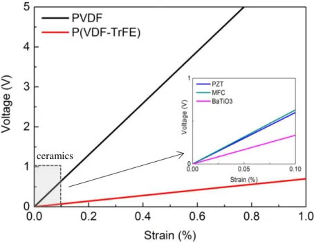
To enlighten this point, we calculated the theoretical voltage output as a function of strain according to equation (1.6) for a selection of piezoelectric materials. The results are shown on Figure 1.16.
Figure 1.16. Theoretical absolute voltage output as function of applied strain for different piezoelectric materials for 1 µm thickness.
Finally, knowing that P(VDF-TrFE) is more appropriate than PVDF for thin film integration, because it does not need to be stretched, it is indeed the best candidate for the realization of flexible thin film piezoelectric harvesters. In addition, research is focused on techniques to improve P(VDF-TrFE) piezoelectric properties. One of them is nanostructuration.
1.2.3 Piezoelectric polymers: nanostructuration
Since piezoelectric properties of PVDF and its copolymers directly depend on the -phase, it is a big challenge for researchers to find a way to increase its content in the polymer material. An even more challenging goal is to control properties at a local scale which can be critical for various nanoscale devices such as nanosensors, non-volatile memories and nanogenerators. There are some works that show that confining these materials with nanostructures allows better control of polymer crystallization in the piezoelectric -phase and in some circumstances orienting these crystallites. Indeed, crystal nucleation is strongly
affected by confining polymer melts into small volumes; the mechanisms involved can be either the exclusion of heterogeneous nuclei or preferential interaction of chains with interfaces [45]. It is therefore possible to control polymer crystallization and increase the content of a particular crystalline phase by nanostructuration depending on the processing conditions. Such nanostructures may also have great potential for high energy density storage applications due to the dramatically increased surface areas over the thin film structure [46]. Different techniques have been applied to produce or pattern organic ferroelectric micro- and nanostructures, including nanoimprint lithography (NIL) [45], [47]–[50], using for example an anodized alumina membrane as a shaping mold [30], [46] or conventional direct drawing (e.g. electrospinning) [51], [52]. Among them, thermal nanoimprint lithography is dominant. It is especially attractive with thermoplastic polymers as a rapid and low-cost technique for the preparation of polymer structures on large areas with feature sizes down to 10 nm [53]. In this technique micro- and nanostructuration is created by the mechanical deformation of a molten polymer film by means of pressing with a hard mold (typically from Si) (Figure 1.17).
Figure 1.17. Schematic drawing of the nanoimprint process of PVDF-TrFE polymer. [50].
The process takes place under vacuum, to avoid air being trapped between sample and mold. The sample is first heated close to the melting point temperature (step 1 and 2 in Figure
1.18). The mold is then pressed to it with a constant pressure of typically 40 bars for several minutes (step 5), while the temperature is decreased (step 3). Once temperature reaches a certain low point, the pressure is released (step 4). The sample is then dissociated of the mold (demolding).
Figure 1.18. Nanoimprint process steps.
The reader may find a more complete state of art of NIL and details about thermo-nanoimprint as used in this work in Cécile Gourgon's article [54], the person who was actively involved in this work at CNRS-LTM.
Because of its potential, this is an exploratory route we will take later in this manuscript. Films of P(VDF-TrFE) will be nanoimprinted in form of fibers after screen printing deposition on interdigital electrodes. The nanoimprint geometry is an inspiration from the structure of MFC macro fiber piezo-ceramic composites which are semi-flexible materials from Smart Material Corp. [55]. The use of such semi flexible piezoelectric materials in our group [34], [56], [57] opened the route of smart composites for energy harvesting that we keep following here towards fully flexible systems.
Thus, next section is a short introduction to composites for energy harvesting with the aim of using fully flexible piezoelectric polymers instead.
1.2.4 Piezoelectric polymers: composites with shape memory alloy
Among the different energy sources, thermal sources are widely available. Usually, thermal energy can be directly converted into electricity by means of thermoelectric [58] (Seebeck effect) or pyroelectric [59] materials. Thermoelectric power generators have already been demonstrated. However, such devices require large spatial temperature gradients with cold source management in order to be efficient. Recently, another concept of thermal-to-electric energy conversion was demonstrated and experimentally approved by our group. It consisted in using hybrid composite structures of semi-flexible ceramic piezoelectric material coupled with shape memory alloy (SMA) [57]. Such coupling aimed on harvesting slow and small temperature variations around a particular temperature threshold which determined by the composition of the alloy.
Numerous metallic alloys exhibit a shape memory effect (SME). Fundamental to this effect is the occurrence of martensitic phase transformation and its subsequent reversal. Basically, a shape memory alloy is deformed in the martensitic phase, and the shape recovery occurs during heating when the alloy undergoes a reverse transformation from martensite to austenite [60]. Both direct and reverse transformations occur within some temperature interval and are characterized by start and finish temperatures. In addition, thermodynamically conditioned thermal hysteresis prevents these temperature intervals from coinciding (Figure 1.19). As a result of this transformation, SMA develops large stress and strain at heating (up to 600 MPa and 10% for NiTi alloy [61]), which can be converted to electrical energy by coupling it with a piezoelectric material, with the mechanical-to-electrical efficiency characterized by coupling coefficient k2.
Since SMAs are able to produce high values of stress (a realistic value is of ~ 4%), it is important to use highly flexible piezoelectric materials which can withstand such high levels of deformation. The combination of both materials can be used for flexible energy harvesting systems. During this work we have realized an energy harvesting prototype by hybridization P(VDF-TrFE) copolymer generators with NiTi-based SMA.
Figure 1.19. Property change vs. temperature for a martensitic transformation
occurring in a shape memory alloy. The parent phase (austenite) is represented by the square lattice, which upon martensitic transformation is distorted into the rhombic martensite phase [60].
1.3 Summary of the targets of this work
The main objective of this work is to demonstrate a functional proof of concept of a flexible thermal smart composite structure able to detect and harvest non-continuous or slow and low thermal events. Here we aimed at hybridizing new screen printed P(VDF-TrFE) piezoelectric microgenerators and existing foils of NiTi-based SMA.
We have seen different approaches of energy harvesting using piezoelectric flexible materials. This is a growing field with many possible commercial applications. Using polymers allows new functionalities where high strain and lightweight are necessary. P(VDF-TrFE) copolymer is the best suitable piezoelectric polymer for screen printing deposition and integration, and it is well adapted for such applications. Moreover, it is possible to further enhance their properties by techniques such as nanoimprint lithography.
In this work we have decided to use new formulated inks of P(VDF-TrFE) for screen printing in collaboration with Liten/Arkema. It was a real challenge initially to fabricate new
efficient flexible piezoelectric microgenerators on plastic substrates. The second challenge was to evaluate under realistic conditions the energy harvesting capabilities of such microgenerators by measuring first the piezoelectric voltage and energy without parasitic losses.
The ultimate target was to produce a functional proof of concept of a fully flexible harvester able to detect non-continuous or slow and low thermal events, which will eventually be events such as small temperature changes in ambient air or due to skin contact. Also, establishing the building blocks to further allow realizing a complete thermal autonomous wireless sensors was in the scope of this work. That is why directions of improvement were part of the final objectives including materials, power management circuit and wireless transmission at the end.
Chapter 2.
Fabrication process for
flexible piezoelectric microgenerators
This chapter presents the materials and methods used to prepare the samples of this study. The full fabrication process flow of the flexible piezoelectric microgenerators is detailed. The experimental work is mainly based on the copolymer of PVDF. The key outcome of this section is the deposition of multilayers of ink-based P(VDF-TrFE) by screen printing. Following the chronology and the progress of the deposition work, we start with a simple single capacitor structure and continue with the design and fabrication of parallel connected capacitors network featuring a credit card format for demonstration. Moreover, to have a broader vision, an exploratory work has been engaged with new inks of terpolymer P(VDF-TrFE-CTFE). This material is known to have relaxor properties with a low hysteresis and high dielectric permittivity at ambient temperature [41], [42]. In particular, original heterostructures of P(VDF-TrFE) and P(VDF-TrFE-CTFE) are realized for the first time. Also, different electrode materials (silver, gold and PEDOT:PSS) are compared to see how they affect the morphology quality of the deposited piezoelectric films.
2.1 Materials and methods
2.1.1 Sample fabrication: overall process flow
In our work the sample fabrication is facing two challenges. One is to develop upstream technological steps and the other is to propose a process flow that meets the needs of industry at the end. That is why the sample fabrication was conducted on the PICTIC platform of Liten which is dedicated to industrial transfer of new printed technologies.
PICTIC has world class research facilities for flexible electronics with 400 m2 class 10’000 clean room (Figure 2.1). It has various equipments for material fabrication and characterization, including an automatic screen printer.
Figure 2.1. The clean room of the PICTIC platform in Liten.
We will now describe the overall process flow of screen printed sample fabrication (schematically presented in Figure 2.2).
Figure 2.2. The overall process flow of sample fabrication.
First γ0 nm Au bottom electrodes were deposited on the 1β5 µm thick flexible organic substrate by using an Alcatel SCM600 physical vapor deposition (PVD) unit. A shadow mask was used for patterning.
Co- and terpolymer layers were deposited from inks by screen printing technique. The total thicknesses varied from 1.1 to 3.9 µm depending on the number of layers deposited. Then, samples were dried for 3 minutes at 60 oC on a hot plate, and then 10 minutes in an infrared oven at 120 oC for terpolymers and at 130 oC for copolymers. These temperatures and
times satisfy conditions for solvent-removal and crystallization of the piezoelectric -phase of P(VDF-TrFE) [62]. The first annealing step at 60 oC was introduced to decrease thermal shock to samples. Without this preliminary annealing we have observed formation of cracks in the P(VDF-TrFE) layer (Figure 2.3).
Figure 2.3. Cracks on the β.6 µm screen printed P(VDF-TrFE) samples without preliminary annealing.
The next step was top electrode deposition by screen printing. Two different materials were used for electrodes: Ag paste (5 µm) or PEDOT:PSS (400 nm). After the deposition, the electrodes were dried the same way as PVDF-based layers.
The last step was the encapsulation of samples with PEDOT:PSS top electrodes. They were covered by a 1 µm protective organic coating using screen printing. This layer is needed to protect PEDOT:PSS as it very sensitive to humidity [63], [64], [65] and keep it on the operating conditions for a long time.
Substrate and its characteristics
A variety of foils are being considered to be used as substrates for flexible electronics taking into consideration their thermal, mechanical and optical properties along with the requirements arising from the various manufacturing processes and operation conditions of the final applications. In general, two classes of substrates are considered: plastic foils and thin metal foils. Thin polymeric foils are extremely attractive for several reasons. First, because they can be made lightweight and inexpensive making it possible to target high-volume and low-cost commercial products. Secondly, processing of these materials being usually carried out at temperatures below 180–1β0 °C makes them particularly attractive for
![Table 1.1. Characteristics of the various printing techniques. Summarized from [6]. Printing techniques Type of printing Viscosity [Pas] Thickness [µm] Throughput [m2/s] Features Inkjet Direct write 0.001–0.04 0.01-20 0.01–0.5](https://thumb-eu.123doks.com/thumbv2/123doknet/12896081.370984/27.892.116.783.129.345/characteristics-techniques-summarized-printing-techniques-viscosity-thickness-throughput.webp)
![Figure 1.8. Power from body-driven sources; total power for each action is included in parentheses [27]](https://thumb-eu.123doks.com/thumbv2/123doknet/12896081.370984/31.892.308.642.267.618/figure-power-driven-sources-total-action-included-parentheses.webp)
![Figure 1.11. Scheme of the experimental set-up used to investigate the direct piezoelectric response of the P(VDF-TrFE) samples [30]](https://thumb-eu.123doks.com/thumbv2/123doknet/12896081.370984/33.892.330.616.103.384/figure-scheme-experimental-investigate-direct-piezoelectric-response-samples.webp)

![Figure 1.17. Schematic drawing of the nanoimprint process of PVDF-TrFE polymer. [50]](https://thumb-eu.123doks.com/thumbv2/123doknet/12896081.370984/42.892.247.691.582.979/figure-schematic-drawing-nanoimprint-process-pvdf-trfe-polymer.webp)


