HAL Id: cea-01483491
https://hal-cea.archives-ouvertes.fr/cea-01483491
Submitted on 6 Mar 2017
HAL is a multi-disciplinary open access
archive for the deposit and dissemination of
sci-entific research documents, whether they are
pub-lished or not. The documents may come from
teaching and research institutions in France or
abroad, or from public or private research centers.
L’archive ouverte pluridisciplinaire HAL, est
destinée au dépôt et à la diffusion de documents
scientifiques de niveau recherche, publiés ou non,
émanant des établissements d’enseignement et de
recherche français ou étrangers, des laboratoires
publics ou privés.
Distributed under a Creative Commons Attribution| 4.0 International License
Patterning of spontaneous rolling thin polymer films for
versatile microcapillaries
Rémy Brossard, Valeriy Luchnikov, Patrick Guenoun, Florent Malloggi
To cite this version:
Rémy Brossard, Valeriy Luchnikov, Patrick Guenoun, Florent Malloggi. Patterning of spontaneous
rolling thin polymer films for versatile microcapillaries. Journal of Polymer Science Part B: Polymer
Physics, Wiley, 2017, 55, pp.721-728. �10.1002/polb.24322�. �cea-01483491�
Patterning of spontaneous rolling thin polymer films
for versatile microcapillaries
R ´emy Brossard
1, Val ´eriy Luchnikov
2, Patrick Guenoun
1, Florent Malloggi
1Abstract
We investigate the spontaneous rolling of polydimethylsiloxane(PDMS) thin films and demonstrate the fabrication of capillaries with topographical and chemical patterns on the inner wall. Thin films of polydimethylsiloxane(PDMS) are either coated by a layer of hard material or have their surface hardened by plasma oxidation. They are then driven out of equilibrium by selective solvent swelling in vapor phase resulting in a tubular rolled-up system. The inner diameter of those is measured as a function of layer thickness for different solvents and capping types. Those results are shown to be in good agreement with Timoshenko theory. Before rolling, the future inner surface can be characterized and functionnalized. We demonstrate topographical and chemical patterning, respectively by embossing and microcontact printing. These methods are very simple and can easily produce cylindrical capillaries with inner diameter between 20 and some hundreds of microns with fully functionnalized inner surface, overcoming many difficulties encountered in conventional soft lithography techniques.
Keywords
Patterning, Microfluidics, Microcapillary, Self-rolling, Microfabrication, Polydimethylsiloxane
1LIONS, NIMBE, CEA, CNRS, Universit ´e Paris-Saclay, CEA Saclay 91191 Gif sur Yvette Cedex, France. 2Institut de Science des Mat ´eriaux de Mulhouse, UMR 7361 CNRS-UHA, 15 rue Jean Starcky, 68057 Mulhouse
1. Introduction
Over the recent years, folding has been extensively used as a remarkable microfabrication method for the design of probes and microfluidic devices, leading to the emerging concept of lab-in-a-tube1. Advantage was taken from reversible fold-ing in actuator applications such as cell capture, soft robots or cantilever based biosensors2;3;4. Initially, metallic and semi-conductor compounds were used. Those systems found applications in many fields such as of photonics5for the
de-sign of optical and magnetic resonators6;7, microfluidics8;9,
synthetic neural circuits10;11and energy12. However a recent
trend and challenge emerged with the fabrication of such sys-tem with polymers13;14;15in order to combine the numerous possibilities of chemical functionnalisation and wide range of available mechanical properties of polymeric materials with the easiness of the fabrication process16. This approach quickly lead to a fair number of advanced applications in various fields such as tissue engineering17, biomimetics18 and microtechnology19. Spontaneous deformations of thin elastic films triggered by in-plane stress can result processes such as wrinkling20;21, creasing22;23but also in self-rolling structures24;25;13. The latter are formed in substrate-free films because of a stress gradient along the film thickness. Here we focus on the formation of self-rolled polydimethylsilox-ane (PDMS) tubes, as a non-lithographic method to design functionalized microcapillaries. Self-rolled tubes are obtained with diameters between 20 µm to 200 µm, a relevant scale for biology and microfluidics applications. Remarkably, while
wrinkling and creasing lead to surface modification of the film26, self-rolling is a transformation of a flat surface to-wards a three dimensional object whose surface is usually unaltered by the process (this aspect is discussed in section
3.2.1). This feature is of primary importance since the
sur-face can be functionalized and fully characterized prior to rolling. So far, most studies reported in the literature focused on electrodes integration13;27;28;29but studies dealing with
other kinds of patterning are scarce.
In this paper, we demonstrate the fabrication of tubes with two kinds of inner patterns. Topographic patterning which can be used for example to alter fluid flow - as in micro-mixing applications30- or for its influence on cell growth31;32. In this work, this topographical patterning is made by an embossing-like method. Chemical patterning is also an important feature since it can be used to locally alter the wetting behavior, local-ize cell adhesion or prevent biofouling33. As a proof of prin-ciple of the latter patterning a fluorescent pattern is fabricated by stamping. In this paper, we also clarify the mechanisms that select the tube size by examining two different bilayer systems. Both are based on a PDMS film of few microns but with different capping layers. In the first case, the surface is hardened by exposure to a low energy oxygen plasma34;29 which is a common technique in soft lithography. In the sec-ond case, we take benefit of the versatility of using polymers by coating a thin film of a biocompatible polymer: chitosan35
is spin coated on PDMS resulting in a film of a few hundreds of nanometers. Rolling occurs when the system is exposed to chloroform29or pentane in gas form. The variation of the
ra-Patterning of spontaneous rolling thin polymer films for versatile microcapillaries — 2/8
dius of curvature as a function of the PDMS layer thickness is measured and the predictive ability of standard rolling model is demonstrated for each of our different methods.
2. Self-rolling instability in a polymer
bilayer system
2.1 Mechanism of self-rolling
Mechanical stress in a material can be generated by many stimuli such as thermal expansion, or solvent exposure. In an homogeneous material, this stress is relaxed by shrinking or swelling. However, in an non-homogeneous material this stress leads to fascinating non flat rest positions36;18.
The case of bilayer thin films was originally considered by Stoney37and Timoshenko38at the beginning of the twen-tieth century. The system of interest is a stacking of two perfectly elastic layers. In an initially flat configuration, the top layer is at rest while the bottom layer swells i.e. it has an embedded compressive strain. Such a system is obviously not at equilibrium. Given L the main thickness of the plate, the bending modulus scales as L3while the stiffness scales
only as L. Hence at small scale, the stress is mainly relaxed by bending. Under small strain, the system will exhibit an isotropic curvature i.e. a sphere portion shape39. However due to geometrical constraints, at larger strain, the symme-try is broken and a preferential bending direction is chosen resulting in a cylindrical shaped object.
Complex analytical and numerical models40;41have been developed to understand the interplay of the two dimensions of the system. However, as long as a rolling direction is chosen by the system, we show here that the original simple result of Timoshenko captures well the features of our system as a first approximation. In the regime of small deformation and considering the two directions of curvature as independent, it can be shown that the relation between the diameter d, curvature κ = 2/d and total thickness of the film h, the strain mismatch δ , the ratio of the layers thicknesses m and elastic moduli n is as follows38: κ =6δ h (1 + m)2 nm3+ n−1m−1+ 4m2+ 6m + 4 with m = hf hs and n =Ef(1 − νs) Es(1 − νf) (1)
Ei, νiand hiare the elastic modulus, the Poisson ratio and the
thickness of the layer i, and the indexes f and s refer to the film and substrate respectively. One has to note that models similar to Stoney model for bending plates measurement give identical results.
2.2 Fabrication scheme
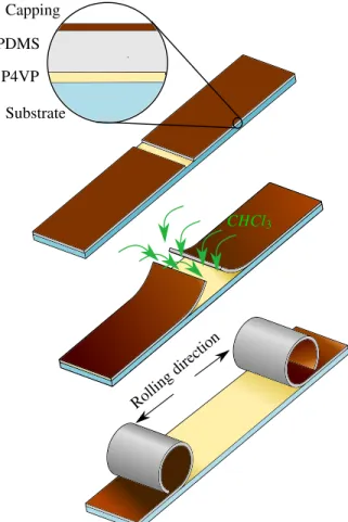
This process aims at the fabrication of PDMS based micro-tubes. Hence, all of the following processes are based on a thin layer of cross-linked PDMS on a layer of poly-4-vynil pyridine (P4VP) which is used as a low adhesion material -on a glass substrate. Capping CHCl3 Rolling direction PDMS P4VP Substrate
Figure 1.Stage of the rolling process.
Then, the fabrication process must include two important steps. First, one has to introduce some sort of inhomogeneity in the system. Second, a stress that follows this inhomogeneity must be produced.
The former task is done by hardening a PDMS thin film surface by either oxidizing it by oxygen plasma exposure or coating it with a hard material which has a good adhesion to PDMS. Plasma treatment results in a silica-like layer of approximately 100nm42. In the second case, we chose chi-tosan - a biocompatible polysaccharide soluble in weak acid-, producing a 270nm layer by spin coating.
Subsequently, a cut is done in the film to define the limits of the film to be rolled. The whole system is then exposed to a solvent that swells PDMS but not the hard layer. In our case, chloroform or pentane is used. As illustrated in figure1, the solvent will preferentially enter through the cut where the free PDMS is exposed and the rolling process occurs.
Once the system is taken out of the solvent, the swelling stimulus quickly disappears. Thus, at large scale (i.e. tubes of several hundreeds micrometers diameter), the system will quickly unroll when taken out of the solvent. However, at smaller scale (i.e. tubes of several tens micrometers diameter), the adhesion of the rolled film on itself is able to hold the tube enclosed.
diam-eter of the tube in that process. The n, m, and δ paramdiam-eters in formula1can be modified by changing the capping and nature of the solvent. All those aspects are discussed in the next section.
3. Results and discussion
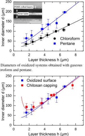
3.1 Influence of the process parameters on the di-ameter 0 2 4 6 8 0 50 100 150 200 250 Inner tube PDMS rolled layers
(a) Diameters of oxidized systems obtained with gaseous chloroform and pentane.
0 2 4 6 8 0 5 0 1 0 0 1 5 0 2 0 0 2 5 0 Oxidized surface Chitosan capping In ne r d ia m et er d (µ m ) Layer thickness h (µm)
(b) Diameters of oxidized and chitosan coated films rolled in pentane gas.
Figure 2.Inner diameters of rolled tubes as a function of total bilayer thickness for different processes.
We applied this fabrication process to PDMS films with a thickness between 1 and 10 µm obtained by spincoating. In order to image the inside of the resulting tube, they are then embedded in a PDMS matrix. Hence, as the optical index does not vary at the external surface of the tube, the inner air/PDMS interfaces can be imaged from above (see inset in figure2a). This technique is used to measure simultaneously the total thickness of the film and the inner diameter. In some cases, for the thicker films, we noted a variation of the thickness of the different layers, which might be due to a secondary relaxation mode, similar to a wrinkling phenomena. If that was the case,
only the thickness of the first layer was measured. If not, the average over all layers was measured.
The inner diameters of tubes is plotted as a function of total thickness of the bilayer in figure2for the different pro-cesses. In figure2a, we compare the diameters obtained in gaseous pentane and chloroform while the influence of the capping is compared in figure2b. The data was averaged over thickness intervals of 1µm. Each point displayed represents the average of 3 to 15 measurements. Hence, the displayed error bars shall be understood as variations of the measured value and not as measurement errors.
For the sake of the confrontation of those results with the predictions of formula1, we need to define several parameters: • The differential strain δ is just the in-plane swelling
ratio of PDMS when the rolling process occurs. • The thickness of the top layer, its elastic modulus E
and Poisson ratio ν in unswollen state were already determined in a previous article42. For the PDMS sub-strate we took EPDMS= 2.6MPa and ν = 0.5. For the oxidized PDMS capping layer we used E = 1.5GPa, ν = 0.5 and hf = 175nm. For the chitosan capping
layer we used E = 3GPa, ν = 0.3 and hs= 270nm.
• As the film swells, the elastic modulus is known to scale as (1 + δ )−143.
• Contrary to the thickness of the PDMS film that we mea-sure without solvent, the one in Timoshenko formula has to be the swollen thickness. As the film is initially constrained in both plane direction and PDMS is incom-pressible, the value to be used is hswollen= (1 + 3δ )hdry.
The only unknown parameter is the swelling ratio itself. We measured it by recording the swelling ratio of a free PDMS film as a function of exposure time to solvent vapor and com-paring it with the time needed of an oxidized pdms film to start rolling. With this method we found that δ is of the order of 5 to 10%. On figure2, we tested the hypothesis that δ is not a function of the thickness h and adjusted its value to fit at best the experimental curve. With values of δ within our estimation, the formula matches very nicely our experimental result. The parameters used with formula1to plot the plain line in figure2are summed up in Table1.
Capping Oxide Chitosan n 448(1+δ ) 824(1+δ ) hf 175 ± 45nm 270 ± 20nm
Solvent Chloroform Pentane δ 9.4% 5.3%
Table 1.Summary of parameters used for the evaluation of formula1for the different processes.
One could note that the value of δ is below values found in literature44;45.Two hypothesis can be made in order to ex-plain this fact. The first one is that the film is only partially
Patterning of spontaneous rolling thin polymer films for versatile microcapillaries — 4/8
swollen when the rolling occurs. This hypothesis leads to a strong dependency of δ in the thickness h that we do not observe, as our results fit better with a constant δ . Hence we reject that hypothesis. The second hypothesis is that the film is saturated in solvent but that for another reason, the saturation limit is lowered. It could be at least partially -explained by the large stress that the rolled system undergoes as it is prevented to swell in-plane46due to the presence of the hard layer. In the stress free case, the swelling ratio is determined by a balance between a mixing free energy of the polymer in the solvent and an elastic energy due to the extension of the polymer chains in the cross-linked network. In the case where in-plane deformations are prevented, the system undergoes forces which make expanding the system even less favourable, preventing the solvent to enter the ma-terial. Moreover the PDMS is slightly porous and it has to be added that poromechanics states that solvent will migrates away from compressed areas. As the swelling ratio of the ma-terial is directly related to the proportion of solvent it contains, its effective value is lowered. Its prediction in this particular case is a difficult problem, as both the stress field and local solvent concentration are unknown and delicate to measure. This problem remains an open question and is out of the scope of this article.
One last thing to note is for a given n, the maximum of curvature in formula1is κ =32δ
hwith m = 1/
√
n. The value of m which results in this largest curvature is in between 0.03 and 0.05. As the optimum is very shallow, an error of up to a factor 3 on m leads to a change in curvature of only 10% in this range of n. In this work, m spans an experimental range between 0.15 and 0.01 so that those systems are close to the minimal radius of curvature to thickness ratio.
3.2 Demonstration of the fabrication of a capillary with patterned inner surfaces
The previously discussed analysis results in the controlled making of tubes with well-defined inner diameters over a wide range, relevant for microfluidic applications. A further step is to pattern the inner surface of the film prior to rolling in order to produce fully patterned cylindrical channels.
3.2.1 Untreated surface state of rolled-up systems
For practical applications, the state of the inner surface of the capillary is of utmost importance. We performed AFM measurements of the surface of our systems. The surface of chitosan is uniform with a root mean square roughness Rq= 1.85nm (data not shown). The plasma oxidized surface
has a similar roughness Rq= 1.53nm. However, cracking of
the surface occurs as shown on figure3. The depth of those cracks is approximately the thickness of the oxide layer and their width is of some microns. In figure3, we also provide the typical profile of one of those cracks.
For practical reasons, this cracking of the surface can be a problem. However, it can be circumvented by coating it with a supplementary PDMS layer before rolling. As the bending rigidity of a film exhibits a cubic scaling in thickness and
distance (µm) heigh t (nm) 0 2 4 6 0 50 -100 -50 cracks 500nm 0
Figure 3.Top AFM image and height profile of a crack on an oxidized PDMS surface. Bottom Optical image of cracks on an oxidized pdms surface during rolling.
linear in elastic modulus, one can easily make the mechanical impact of this film negligible by making it thin and soft -for example by diminishing the cross-linker concentration in PDMS-. This step is necessary in particular when very small pattern are to be designed on the surface of the capillary.
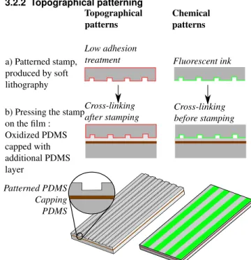
3.2.2 Topographical patterning Patterned PDMS Capping PDMS Topographical patterns Cross-linking after stamping b) Pressing the stamp
on the film : Oxidized PDMS capped with additional PDMS layer Low adhesion treatment Chemical patterns a) Patterned stamp, produced by soft lithography Fluorescent ink Cross-linking before stamping
Figure 4.Process steps for the topographic patterning of a system before rolling.
Prior to rolling, the future inner surface of the tube can be functionnalized to obtain 3D patterned systems.
First, we demonstrate an embossing-like method to ob-tain topographical patterns. In a first step, a PDMS negative replica of the desired patterns is produced by soft lithogra-phy that we call the stamp. It is then functionnalized with (1H,1H,2H,2H-perfluorooctyl)trichlorosilane, which serves as a low adhesion coating. The stamp can then be pressed
against an uncrosslinked PDMS film so that reticulation oc-curs against the stamp. The desired structure is obtained once the stamp is removed.
The process is sketched in figure4and the obtained capil-laries are displayed in figure5.
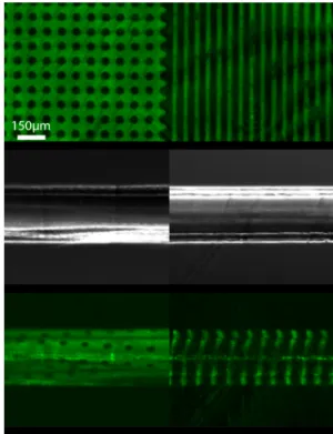
Figure 5.Topographical patterned. Top 2.1 µm deep, 10 µm and 40 µm wide pillars on a 11.5 µm rolled film.Bottom 11.5µm deep, 50 µm wide grooves on a 48 µm rolled film.
3.2.3 Chemical patterning
The very similar scheme of microcontact printing can be used to produce chemical patterns (see4). A PDMS stamp is also produced by soft lithography and inked with a solution of polylysine grafted polyethylene glycol(PLL-g-PEG) labeled with a green fluorescent probe. An oxidized PDMS layer with an additional soft PDMS coating is produced as before. It is exposed briefly to plasma in order to activate the surface with-out altering its mechanical properties. The stamp is dropped on this surface and left for 5 minutes. Circular holes with diameters of 40 µm and 10 µm wide lines are stamped on the flat film. The film can then be rolled normally. The resulting systems were imaged with fluorescent microscopy techniques as displayed on figure6. Rolled-up systems are imaged far from the substrate plane so that only the patterns in the tube are seen.
The pattern in the latter case is only adsorbed to the surface and has a limited resistance in time. However, this method can in principle be adapted to any other microcontact print-ing method for glassy substrate in order to obtain a covalent bonding of the pattern as in Abdullah et al.47.
4. Conclusion
Spontaneous curvature is induced in capped PDMS thin film by selective solvent swelling. That method is used as a non-lithographic mean to obtain self-rolled micro-capillaries with an inner diameter between 20 and 200 µm. The obtained di-ameter as a function of film thickness was optically measured for different solvent chloroform and pentane and capping -PDMS oxide and chitosan -.
Those results are confronted to Timoshenko model. Al-though one parameter is only known in term of order of
Figure 6.Fluorescence images of stamped system Top before and Bottom after rolling. Middle Rolled up system in bright field imaging.
magnitude, the predictive ability of the model seems very satisfactory.
The striking feature of that system is that the future inner surface of those tubes is initially accessible so that it can be properly characterized or functionnalized before rolling. The different surfaces state resulting from the different capping were imaged by AFM. Examples of topographical and chemi-cal patterning were performed as a concept demonstration.
In the context of microfluidic, soft lithographic methods are widely used because designs based on channel shapes - T or Y junctions, flow focusing - are easy to fabricate. However, techniques requiring further surface specialization - grooved surface, local change in wetability, cell adsorption - can re-quire a lot more efforts. On the contrary, self-rolled polymer capillaries present great hope for the trivial design of special-ized capillaries, but only tubular channels are obtained. Hence, the establishment of hybrid methods taking advantage of both techniques could be a new route to broaden the possibilities of microfluidic chip design. Such methods are currently under investigation.
5. Experimental
5.1 Material
PDMS elastomer was purchased from Dow Corning (Sylgard 184). P4VP, chitosan, silane and solvents were purchased from Sigma Aldrich, polylysine(20 kDa) grafted with polyethylene glycol(2 kDa) and labeled with fluorescein isothiocyanate (PLL-g-PEG/FTIC) was purchased from Susos.
Patterning of spontaneous rolling thin polymer films for versatile microcapillaries — 6/8
5.2 Film fabrication
Glass substrates are cleaned by UV-Ozone, plasma and acid technique48to get reproducible wetting and surface state. A
solution of P4VP in ethanol (1 g.L−1) is spin coated on the substrate at 3000 RPM for 30 seconds with an acceleration of 500 RPM.s−1.
Sylgard PDMS is mixed with the furnished cross-linker with a ratio 10:1. After degazing, this mixture was either directly spin coated for the fabrication of layers thicker than 10 µm or further diluted in toluene in proportion 3:1, 1:1 and 3:1 in order to reduce the viscosity of the solution for the fabrication of thinner layers.
Thicker films are obtained by spin-coating on the substrate with three steps. First, a step at 500 RPM for 30 seconds is done to spread PDMS uniformly on the substrate. Second, a step at various speeds for 5 minutes takes place in order to adjust the film thickness (typically, with a speed of 3000 RPM, a thickness of 12.8 µm is obtained. Finally for thicker films, a 2 second pulse at 5000 RPM is used to remove the edge beads. The acceleration is 3000 RPM.s−2
Thinner films are obtained by spin-coating of diluted PDMS on the substrate at various speeds between 3000 RPM and 10000 RPM for one minute with an acceleration on 500 RPM.s−1.
The samples are then placed on a hot plate at 150◦Cfor 15 minutes to ensure a quick evaporation of toluene and a complete cross-linking of the material.
5.3 Capping fabrication
Oxidized PDMS samples are prepared in a Harrick’s plasma cleaner. Oxygen is supplied to the chamber where the pressure is regulated by the equilibrium between the oxygen entrance flow rate (monitored with a microvalve) and a fixed outflow. The pressure is set to 4.10−1mbarand the plasma is powered on at 29.6 W for 40 minutes. An additional PDMS layer can eventually be spin-coated above this oxide layer as in4. The PDMS to cross-linker ratio used is 1:20 and its typical thick-ness is one third to one fourth of the carrier film thickthick-ness.
Chitosan is dissolved in chlorhydric acid (pH = 1). The dissolution process is slow and can be accelerated by ex-tended sonication. In order to prepare chitosan on PDMS samples, those are exposed to plasma for one minute to make the surface hydrophilic. The chitosan solution can then be spin-coated on the substrate at 500 RPMfor one minute with an acceleration on 500 RPM.s−1. The samples are then dried for one hour at 80◦Con a hot plate.
5.4 Rolling
The film is first cut in order to release the borders of the future tube. It is then placed in a closed glass petri dish filled with a few milliliters of solvent. Two small pillars maintain the system a few millimeters away from the solvent, the film di-rectly facing its surface. In those conditions, the rolling occurs within minutes. For thicker systems, the system often rolls back once taken of the solvent. The stability of the tube can be increased by a liquid phase annealing in the same solvent
for a few hours which makes the deformation only partially reversible. This annealing step was never performed for the measurement of inner diameter as a function of experimental parameters.
5.5 Topographic patterning of a PDMS film
A PDMS 5 mm stamp is fabricated by conventional soft lithog-raphy techniques49. The surface of the stamp is activated with oxygen plasma for 2 minutes. The stamp is then placed for 12 hours in a closed 4 inches wide petri dish with 10 µL of (1H,1H,2H,2H-perfluorooctyl)trichlorosilane. Before its use, The stamp is degazed at 0.1 mbar for at least 10 minutes
A PDMS film of desired thickness is obtained as above Before the cross-linking of the PDMS occurs, the stamp is carefully applied against the film so that large bubbles are avoided (small bubbles will disappear if the stamp was prop-erly degazed). The system and stamp are then placed on a hot plate at 80◦Cfor an hour. In order to prevent unsticking of the stamp due to thermal effects, a weight of 500 grams is put on the sample during the reticulation process. After cooling down of the system the stamp is carefully removed. This step is tricky has the fragile film is lowly adhesive on both the substrate and the stamp. This step is greatly facilitated by adding a few drops of ethanol at the edge of the stamp which instantly causes the delamination of the stamp. However, one should be careful that ethanol does not reach the substrate as P4VP is soluble in ethanol.
Two cases are described in this paper. The first case is to stamp the first layer of PDMS which can then be oxidized and rolled as above. The second case is to stamp an additional thinner and softer PDMS layer on an oxidized ready to roll layer. It can then directly be cut and rolled as above. The former method is more suitable for large systems, while the latter is essential to design very small structures which would be damaged by exposure to plasma.
5.6 Microcontact printing
A stamp was designed with soft lithography techniques49. A few drops of aqueous solution of PLL-g-PEG/FTIC 0,1 mg/L are poured on the stamped and spread by pressing a glass slide on top of it. After 5 minutes of infusion, the stamp is dried with nitrogen until no solvent remains. A ready to roll film with an additional layer of soft PDMS is designed as above. It exposed to oxygen plasma with an for 2 minutes. The stamp is dropped on the activated surface and left for 10 minutes. The system can then be rolled as above.
5.7 Size measurements and imaging
Tube were encased in PDMS and optically imaged with an optical transmission microscope. The images were treated with imageJ software to measure simultaneously the thickness of the film and the diameter of the tube. Patterned systems in inset of figure2awere imaged with an Dino-lite numer-ical microscope. Both the thickness of the film and the 3-dimensionnal shape of the patterns were measured with an optical interferometer. The surface state of the systems were
imaged with an AFM Dimension V (Digital Instruments / Veeco-Bruker , Santa Barbara, CA, USA) in contact mode. Fluorescence was imaged with an Olympus Fluoview FV1000 inverted confocal microscope.
6. Acknowledgments
This work was supported by the French National Research Agency, Grant no ANR-13-IS09-0002.
References
[1] E. J. Smith, W. Xi, D. Makarov, I. Monch, S. Harazim,
V. A. Bolanos Quinones, C. K. Schmidt, Y. Mei, S. Sanchez and O. G. Schmidt, Lab Chip, 2012, 12, 1917– 1931.
[2] J. Zang and F. Liu, Nanotechnology, 2007, 18, 405501. [3] J. Fritz, analyst, 2008, 133, 855–863.
[4] R. Raiteri, M. Grattarola, H.-J. Butt and P. Skl´adal,
Sen-sors and Actuators B: Chemical, 2001, 79, 115–126.
[5] S. Schwaiger, A. Rottler and S. Mendach, Advances in
OptoElectronics, 2012, 2012,.
[6] W. Huang, X. Yu, P. Froeter, R. Xu, P. Ferreira and X. Li,
Nano letters, 2012, 12, 6283–6288.
[7] X. Li, Advances in Optics and Photonics, 2011, 3, 366–
387.
[8] D. J. Thurmer, C. Deneke, Y. Mei and O. G. Schmidt,
Applied physics letters, 2006, 89, 223507.
[9] A. Prinz, V. Y. Prinz and V. Seleznev, Microelectronic
engineering, 2003, 67, 782–788.
[10] P. Froeter, Y. Huang, O. V. Cangellaris, W. Huang, E. W.
Dent, M. U. Gillette, J. C. Williams and X. Li, ACS nano, 2014, 8, 11108–11117.
[11] M. Yu, Y. Huang, J. Ballweg, H. Shin, M. Huang, D. E.
Savage, M. G. Lagally, E. W. Dent, R. H. Blick and J. C. Williams, ACS nano, 2011, 5, 2447–2457.
[12] J. Deng, H. Ji, C. Yan, J. Zhang, W. Si, S. Baunack, S.
Os-wald, Y. Mei and O. G. Schmidt, Angewandte Chemie, 2013, 125, 2382–2386.
[13] V. Luchnikov, O. Sydorenko and M. Stamm, Advanced
Materials, 2005, 17, 1177–1182.
[14] K. Kumar, V. Luchnikov, B. Nandan, V. Senkovskyy and
M. Stamm, European Polymer Journal, 2008, 44, 4115– 4121.
[15] A. Egunov, J. Korvink and V. Luchnikov, Soft matter,
2016, 12, 45–52.
[16] V. Luchnikov, M. Stamm et al., Macromolecular rapid
communications, 2011, 32, 1943–1952.
[17] S. Zakharchenko, E. Sperling and L. Ionov,
Biomacro-molecules, 2011, 12, 2211–2215.
[18] L. Ionov, Journal of Materials Chemistry, 2012, 22,
19366–19375.
[19] Y. Mei, A. A. Solovev, S. Sanchez and O. G. Schmidt,
Chemical Society Reviews, 2011, 40, 2109–2119.
[20] A. E. Shyer, T. Tallinen, N. L. Nerurkar, Z. Wei, E. S. Gil,
D. L. Kaplan, C. J. Tabin and L. Mahadevan, Science, 2013, 342, 212–218.
[21] J. Genzer and J. Groenewold, Soft Matter, 2006, 2, 310–
323.
[22] S. Cai, D. Chen, Z. Suo and R. C. Hayward, Soft Matter,
2012, 8, 1301–1304.
[23] F. Weiss, S. Cai, Y. Hu, M. K. Kang, R. Huang and Z. Suo,
Journal of Applied Physics, 2013, 114, 073507.
[24] V. Y. Prinz, V. Seleznev, A. Gutakovsky, A. Chehovskiy,
V. Preobrazhenskii, M. Putyato and T. Gavrilova, Physica E: Low-dimensional Systems and Nanostructures, 2000, 6, 828–831.
[25] R. Songmuang, C. Deneke and O. Schmidt, Applied
physics letters, 2006, 89, 223109.
[26] S. Yang, K. Khare and P.-C. Lin, Advanced Functional
Materials, 2010, 20, 2550–2564.
[27] V. Luchnikov and M. Stamm, Physica E:
Low-dimensional Systems and Nanostructures, 2007, 37, 236– 240.
[28] K. Kumar, B. Nandan, V. Luchnikov, E. B. Gowd and
M. Stamm, Langmuir, 2009, 25, 7667–7674.
[29] L. P. Chia G´omez, P. Bollgruen, A. I. Egunov, D. Mager,
F. Malloggi, J. G. Korvink and V. A. Luchnikov, Lab on a Chip, 2013, 13, 3827.
[30] A. D. Stroock, S. K. Dertinger, G. M. Whitesides and
A. Ajdari, Analytical Chemistry, 2002, 74, 5306–5312.
[31] E. Martinez, E. Engel, J. Planell and J. Samitier, Annals
of Anatomy-Anatomischer Anzeiger, 2009, 191, 126–135.
[32] A. B´eduer, L. Vaysse, E. Flahaut, F. Seichepine, I.
Loubi-noux and C. Vieu, Microelectronic Engineering, 2011, 88, 1668–1671.
[33] R. Marie, J. P. Beech, J. V¨or¨os, J. O. Tegenfeldt and
F. H¨o¨ok, Langmuir, 2006, 22, 10103–10108.
[34] S. B´efahy, P. Lipnik, T. Pardoen, C. Nascimento, B. Patris,
P. Bertrand and S. Yunus, Langmuir, 2010, 26, 3372– 3375.
Patterning of spontaneous rolling thin polymer films for versatile microcapillaries — 8/8
[35] T. Nishino, R. Matsui and K. Nakamae, Journal of
Poly-mer Science Part B: PolyPoly-mer Physics, 1999, 37, 1191– 1196.
[36] H. Li, PhD thesis, UNIVERSITY OF MINNESOTA,
2012.
[37] G. G. Stoney, Proceedings of the Royal Society of
Lon-don. Series A, Containing Papers of a Mathematical and Physical Character, 1909, 82, 172–175.
[38] S. Timoshenko, JOSA, 1925, 11, 233–255.
[39] N. Salamon and C. B. Masters, International journal of
solids and structures, 1995, 32, 473–481.
[40] S. Alben, B. Balakrisnan and E. Smela, Nano letters,
2011, 11, 2280–2285.
[41] N. Guyot, Y. Harmand and A. M´ezin, International
jour-nal of solids and structures, 2004, 41, 5143–5154.
[42] B. Sarrazin, R. Brossard, P. Guenoun and F. Malloggi,
Soft Matter, 2016, 12, 2200–2207.
[43] M. Rubinstein and R. Colby, Polymers physics, Oxford
Oxford, UK, 2003, vol. 767.
[44] J. N. Lee, C. Park and G. M. Whitesides, Analytical
chemistry, 2003, 75, 6544–6554.
[45] C. Rumens, M. A. Ziai, K. Belsey, J. C. Batchelor and
S. J. Holder, Journal of Materials Chemistry C, 2015, 3, 10091–10098.
[46] K. Dusek, A. Choukourov, M. Duskova-Smrckova and
H. Biederman, Macromolecules, 2014, 47, 4417–4427.
[47] N. H. Abdullah, W. A. W. A. Bakar, R. Hussain, M. B.
Bakar, M. Mohamed, M. K. A. A. Razab and J. H. van Esch, ARPN, 2006, 10, 9538–9543.
[48] W. Kern, Journal of the Electrochemical Society, 1990,
137, 1887–1892.
[49] Y. Xia and G. M. Whitesides, Angewandte Chemie