HAL Id: hal-00966660
https://hal.archives-ouvertes.fr/hal-00966660
Submitted on 27 Jun 2018
HAL is a multi-disciplinary open access
archive for the deposit and dissemination of sci-entific research documents, whether they are pub-lished or not. The documents may come from teaching and research institutions in France or abroad, or from public or private research centers.
L’archive ouverte pluridisciplinaire HAL, est destinée au dépôt et à la diffusion de documents scientifiques de niveau recherche, publiés ou non, émanant des établissements d’enseignement et de recherche français ou étrangers, des laboratoires publics ou privés.
Confined phase separation in SiO_X nanometric thin
layers
M. Roussel, E. Talbot, Cristelle Pareige, R.P. Nalini, Fabrice Gourbilleau,
Philippe Pareige
To cite this version:
M. Roussel, E. Talbot, Cristelle Pareige, R.P. Nalini, Fabrice Gourbilleau, et al.. Confined phase separation in SiO_X nanometric thin layers. Applied Physics Letters, American Institute of Physics, 2013, 103, pp.203109. �10.1063/1.4830375�. �hal-00966660�
Confined
phase separation in SiO
Xnanometric
thin layers
M. Roussel,1E. Talbot,1,a)C. Pareige,1R. Pratibha Nalini,2F. Gourbilleau,2and P. Pareige1
1
Groupe de Physique des Mat!eriaux (GPM) UMR 6634, Normandie Universit!e, Universit!e et INSA de Rouen-CNRS, Av. de l’Universit!e, BP 12, 76801 Saint Etienne du Rouvray, France
2
Centre de Recherche sur les Ions, les Mat!eriaux et la Photonique (CIMAP), CEA/CNRS/ENSICAEN/UCBN, 6 Bd. Mar!echal Juin, 14050 Caen Cedex 4, France
Phase separation in silicon-rich silica/silica multilayers was investigated using Atom Probe Tomography and Atomistic Kinetic Monte Carlo simulation. It is shown that the thickness of silicon-rich silicon oxide sublayers plays an important role during phase transformation. It determines the morphology of Si-rich phase formed after subsequent annealing, which is of prime interest for microelectronic and optoelectronic applications. Monte Carlo simulation reveals that the formation of isolated Si clusters can be achieved even in the case of spinodal decomposition and is directly related to the ratio between the spinodal wavelength and the sublayer thickness.
Because of its indirect band gap, silicon had never been considered for optoelectronic applications until 1990, when Canham showed that nanoporous silicon exhibits intense photoluminescence at room temperature.1Since this discov-ery, Si nanostructures have been intensively studied for their optical and electrical properties.2Among these structures, Si nanoparticles (Si-nps) embedded in silica (SiO2) appears to
be a promising system for optoelectronics and microelec-tronics and could be applied in future generations of solar cells,3 waveguide amplifiers,4 and non-volatile memories,5 as it is suggested by hundreds of recent scientific articles. This enthusiasm is mainly due to the fact that Si-nps embed-ded in SiO2are easily obtained by phase separation between
Si and SiO2in Si-rich silica (SiOX) thin films during thermal
annealing, which is fully compatible with the current silicon technology. In the meantime, many studies have demon-strated that the use of Si-nps requires an accurate control of the particle characteristics and the surrounding oxide quality.1,6–8 Consequently, the formation mechanism of Si-nps in SiOXis of prime interest, since it controls all the
relevant parameters (shape of the Si-nps, diameter of the par-ticles, interface with the surrounding oxide). Recently, it has been evidenced that phase separation mechanisms depend on Si supersaturation. At low Si excess, formation of Si-nps is initiated by nucleation reaction followed by growth re-gime9,10while at higher concentration interconnected Si-rich
nanostructures formed by spinodal decomposition
appear.11,12 The limit between these two mechanisms is defined by the spinodal concentration limit which is close to 30% of Si excess in silica.11,12Finally, in both cases, at late stage (i.e., when the compositions of both phases have reached their equilibrium values), Ostwald ripening occurs.13 Our investigation focuses more precisely on the phase sepa-ration in multilayered structures consisting of a successive stacking of SiOXand SiO2sublayers. This kind of structure
is commonly used in order to control Si-np size distribution14 because the SiO2sublayers are supposed to act as diffusion
barriers. It results in the formation of silicon nanoparticles
having a diameter roughly equal to the thickness of the SiOX
sublayer. The goal of the present study is to understand the phase separation process occurring in such a confined thin film. For that purpose, Atom Probe Tomography (APT) was used in order to analyze various sets of multilayers systems and study the influence of SiOXsublayer thickness. In
addi-tion, we have performed Atomistic Kinetic Monte Carlo (AKMC) simulations of phase separation in binary system in both bulk and thin film configurations. These simulations allow improving the fundamental understanding of the spino-dal decomposition regime in thin SiOXfilms and the
result-ing microstructure.
A set of SiOX/SiO2multilayers (MLs) was deposited on
[100] oriented silicon wafer using reactive radio frequency magnetron co-sputtering. Si and SiO2targets were used for
SiOXsublayers deposition under hydrogen-rich plasma while
pure silicon oxide sublayers were deposited by sputtering pure silica target under Ar plasma. The MLs were grown at 500!C with a power density of 2.2 and 7.4 W"cm#2applied on the Si and SiO2targets, respectively. The sputtering time
permitted to tune SiOXand SiO2sublayer thicknesses. More
details about the synthesis of SiOX/SiO2MLs by magnetron
sputtering can be found in Ref. 14. Two different sets of
MLs were prepared. Sample A: SiOX-4 nm/SiO2-3 nm;
Sample B: SiOX-8 nm/SiO2-10 nm. The silicon excess in
SiOX sublayers is the same in both set of samples and is
measured to be 31%. Finally, to form Si-ncs, these samples have been submitted to various annealing treatments under N2atmosphere. TableIsummarizes the different sets of
mul-tilayers and their respective annealing treatment.
APT experiments were performed using a Laser
Assisted Wide Angle Tomographic Atom Probe
(LAWATAP, CAMECA) using UV (343 nm) femto-second laser pulses (50 nJ, 350 fs). A full description of atom probe tomography technique can be found in Ref.15, for example. Specimens for APT were prepared using a Dual-beam SEM-FIB NVision 40 (ZEISS) avoiding the incorporation of Gaþ ions in the specimens during sample preparation. The details of the standard procedure are reported in previous works.16,17 As it has been already demonstrated in previous works, APT
is a powerful technique for giving a detailed microstructure at the atomic scale level of silicon nanoclusters in a SiO2
host matrix.10,18Sample A was used to perform a complete kinetic study of the spinodal decomposition. Since it contains 31% of silicon excess, it is expected to decompose via a spi-nodal regime.12It was annealed at 900!C for times ranging
from 15 min up to 20 h (samples A1–A6). The corresponding
APT reconstructions are presented in Fig.1. As shown from Figs.1(a)–1(e), a typical interconnected structure develops with ageing time. But the morphology changes after an annealing time of 20 h at 900!C. Fig.1(f) reveals isolated
Si-nps. This microstructure may originate from two different phenomena which will be discussed in detail hereafter: (i) it can be the signature of a late stage coarsening regime. Indeed, the compositions of both phases have reached their equilibrium values. The major contribution to the driving force for unmixing in that case is the reduction of surface interphases between the two phases. Consequently, for a vol-ume fraction lower than the percolation threshold, isolated particles are observed. (ii) It may stem from the confined characteristic of the thin layers in which the decomposition process takes place.
The influence of SiOX sublayer thickness has been
investigated by comparing the microstructure of two sets of sample containing #4 nm SiOX sublayers (A3, A7, and A8)
and 8 nm SiOXsublayers (B1, B2, and B3) after an annealing
treatment at 900!C, 1000!C, and 1100!C during 1 h. Both samples (Ai and Bi) contain 31% of Si excess. APT results
are presented in Fig.2. In the case of 8 nm-thick SiOX
sub-layers Figs. 2(a)–2(c), spinodal decomposition is indeed observed whatever the thermal budget. However, in the case of 4 nm-thick SiOXsublayers, increasing the annealing time
has a remarkable influence: the interconnected structure is no longer observed at 1000!C and 1100!C and isolated Si-nps have been formed Figs.2(d)–2(f). These Si-nps have sharp interfaces and have a mean radius of 1:6 6 0:1 nm. Once again, two assumptions can be proposed on the forma-tion of Si-nps: (i) Increasing the annealing temperature leads to a change in decomposition mechanism (from spinodal decomposition at 900!C to nucleation followed by growth at 1100!C). Nevertheless, as it is reported in Ref. 12, due to the extremely low solubility limit of Si in SiO2and the Si-O
phase diagram, one can expect that the spinodal concentra-tion limit does not vary between 900!C and 1100!C.19 (ii) Spinodal decomposition takes place in all samples and the formation of isolated Si-nps is due to the thickness of the SiOXsublayer.
APT investigation strongly suggests an influence of the thickness of SiOXsublayers on the decomposition process in
the analysed systems. Nevertheless, a quantitative descrip-tion of this phenomenon is still missing. For instance, we cannot predict a critical value for the thickness of SiOX
layers under which Si-nps will form. This is mainly due to the fact that a quantitative description of the spinodal decom-position is usually achieved by determining the decomposi-tion wavelength using autocorreladecomposi-tion profiles.20In our case, the peculiar geometry of the sample and, more particularly, the thin layer thickness analyzed prevents such a measure-ment. In order to provide a better understanding of the phe-nomenon, we developed atomistic Atomistic Kinetic Monte Carlo simulations.
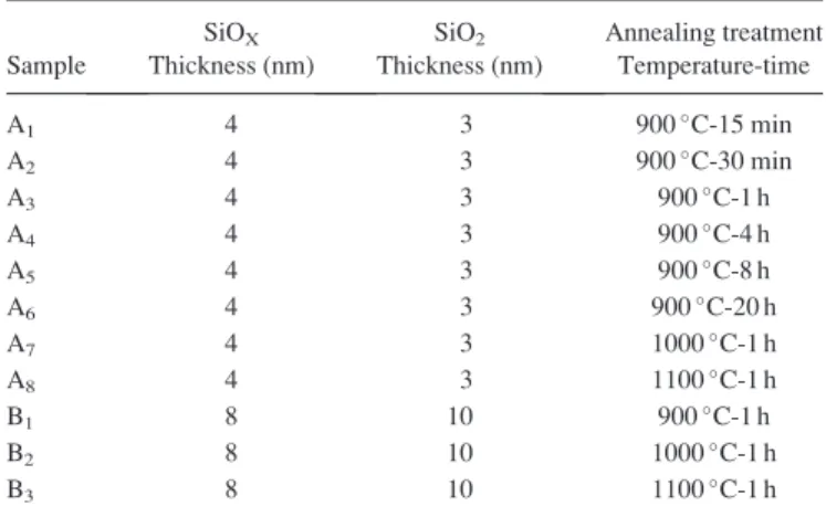
TABLE I. Layer thicknesses and heat treatment for each multilayer.
SiOX SiO2 Annealing treatment
Sample Thickness (nm) Thickness (nm) Temperature-time
A1 4 3 900!C-15 min A2 4 3 900!C-30 min A3 4 3 900!C-1 h A4 4 3 900!C-4 h A5 4 3 900!C-8 h A6 4 3 900!C-20 h A7 4 3 1000!C-1 h A8 4 3 1100!C-1 h B1 8 10 900!C-1 h B2 8 10 1000!C-1 h B3 8 10 1100!C-1 h
FIG. 1. Decomposition kinetics in SiOX layers containing 31% of Si
excess and annealed at 900!C for: (a) 15 min (sample A1); (b) 30 min (sample
A2); (c) 1 h (sample A3); (d) 4 h (sample
A4); (e) 8 h (sample A5); (f) 20 h
(sam-ple A6). Si-rich phase is evidenced
using 55 at. % of Si isoconcentration surfaces. Volumes: 12% 12 % 4 nm3.
Mulleret al. have used KMC to evidence a transition of phase separation mechanism from nucleation-growth to spi-nodal decomposition as a function of Si implantation doses in pure silica.11,21 Besides, spinodal decomposition and phase separation have been theoretically or numerically investigated in constrained films.22–24 Drawing inspiration from these works, we propose to combine our APT results with AKMC simulations in order to clarify the origin of the formation Si-nps through spinodal decomposition.
Modelling the kinetics of phase transformation between Si-rich and SiO2phases is a very complicated task because
of the complexity of the system. To give just few major locks: non-isostructural structures of the two phases, ordered structure of SiO2, amorphous structure of silica, and
associ-ated complex diffusion mechanisms in amorphous structure. Consequently, this accurate AKMC modelling does not exist, starting with a simplified model is a useful first step. As our goal was to study the evolution of spinodal decomposition confined in a nanometric layer and to get a reliable descrip-tion of the kinetic of precipitadescrip-tion for confined thin layers, an AKMC model already developed to accurately simulate spi-nodal decomposition in binary AB alloy has been used.20,25 Thus, the amorphous nature of the real material and diffusion mechanism which occurs in silica matrix have been neglected. The diffusion of atoms is based on thermally acti-vated jumps of one vacancy towards one of its nearest neigh-bour atoms. The simulated crystals are constructed on a rigid BCC lattice. A and B atoms and one vacancy are distributed
overN¼ L2% h cells. L corresponds to the planar dimension
(L¼ 64a0witha0the lattice parameter of the BCC structure)
whileh corresponds to the thickness of the simulated layer. h varies between 8a0 and 64a0 (hereafter referred to as
8 … 64). Periodic boundary conditions are applied in the plane directions. Along the growth axis, boundaries act as walls in order to account for the presence of SiO2layers which play
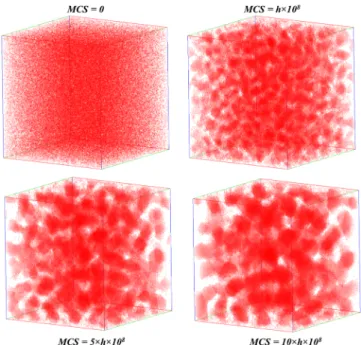
the role of diffusion barriers. Neither the vacancy nor the atoms can pass through these boundaries. The model relies on the residence time algorithm26to model the diffusion of the vacancy and is fully described in Refs. 20and25. As it has been explained before, one of the information that we cannot extract from APT analyses is the wavelength of the composi-tion fluctuacomposi-tions, because of the peculiar geometry of the sam-ple. AKMC simulations in the bulk case permit to overcome this problem. A reference simulation was performed in a bulk A-B system containing 30% of B species. It provided the B-rich phase fluctuation wavelengths for different simulation times in non-constrain case. AKMC simulations have been performed over 643cells. In this case only, periodic boundary conditions were applied in the 3 spatial directions. The initial configuration of A and B species was chosen random. The 3D distributions of B atoms in the system aged for 0 Monte Carlo Steps (MCS) up to 10% 64 % 108 MCS are shown in Fig.3. The measured wavelengths are reported in Table II. These values will permit to quantify the development of spinodal decomposition for each simulated time.
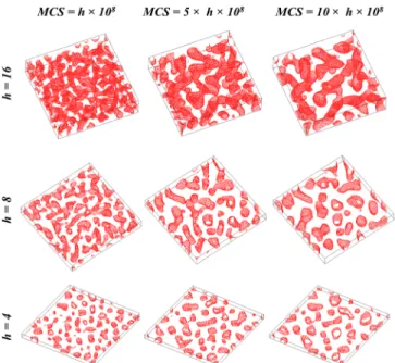
In order to clearly identify the influence of the thickness of the layer on the decomposition process, simulations were undertaken in thin layer configuration for the same alloy than in the previous case (i.e., 30% of B atoms). The simu-lated volume contained L¼ 642 cells in the plane of the
layer while the thicknessh varies from 4 to 16 cells.
Figure4shows the ageing evolution of the structure of B atoms as function of the thickness. (i) For the thickest layer (h¼ 16), ageing evolution is comparable to the bulk
FIG. 2. Volume reconstructions of SiOXsublayers for different annealing
treatments and SiOX sublayer thicknesses. (a)–(c) SiOX¼ 8 nm; (d)–(f)
SiOX¼ 4 nm. Red dots correspond to silicon atoms and green ones
corre-spond to oxygen atoms. Si-rich phase containing more than 55 at. % of Si atoms appears as bold red dots. Volumes: 12% 12 % 8 nm3 and 12% 12 % 4 nm3.
FIG. 3. AKMC simulation of spinodal decomposition in a bulk A-B system containing 30% of atom B, for different ageing times. Only B atoms are rep-resented. The simulated volumes contain 64% 64 % 64 BCC cells.
case. An interconnected structure developed during ageing. (ii) For the intermediate case (h¼ 8), we observe that after MCS¼ 5 % h % 108, the interconnected structure is lost to
the benefit of B-pure isolated regions (B-nps). This effect is more pronounced atMCS¼ 10 % h % 108. It is worth to note
that this kinetic reproduces the experimental one observed in sample A2to A6(Fig.2). (iii) Concerning the thinnest layer
(h¼ 4), B-pure isolated regions are observed since the first ageing times. No development of an interconnected micro-structure is observed. These simulated kinetics reproduce remarkably well the experimental observations. To under-stand the behaviour of decomposition in a thin layer, we have compared the thickness of the layer with the fluctuation wavelength (estimated for the bulk). For the thickest layer, the thickness (h¼ 16) is always higher than the fluctuation wavelength which reachesk ¼ 15:3a0. In this case as in the
bulk case, an interconnected structure is still observed after 10% h % 108MCS. It is important to note that, after this age-ing time, no isolated particles that would be representative of the late stage of coarsening regime are observed.
For the intermediate case (h¼ 8), isolated B-nps appear when the wavelength becomes higher than the sublayer
thickness. This phenomenon appears as soon as MCS
¼ 5 % h % 108 (where
k ¼ 11:9) and is even more pro-nounced forMCS¼ 10 % h % 108 (where
k ¼ 30:6). As no late stage coarsening is expected after this ageing time as discussed above, the simulations show that the appearance of these isolated objects originates from the confinement in the thin layer. These results strongly suggest that the presence of
the isolated Si-nps after 20 h of ageing at 900!C in SiOX
sublayers containing 31% of excess Si (Fig.2) is a size effect and not a kinetic effect (late stage of coarsening). It is clearly a consequence of the development of spinodal decomposi-tion in a constrained layer. Finally, for the thinnest layer (h¼ 4), the wavelength is always higher than the thickness and B-nps are always observed. From these results and owing to the comparison of the ratio between bulk fluctua-tion wavelengths (TableII) and layer thicknesses for the dif-ferent cases, one can conclude that isolated B-nps are present whenk=h > 1, which is in good agreement with phase field simulations performed by Seolet al.22This understanding of nanostructural changes in confined systems is of great impor-tance for the development of high quality and performance of devices. In addition, besides the development needed to more accurately simulate these systems (on going work), this approach can easily be extended to other confined systems.
Owing to the fruitful comparison of APT experimental results and AKMC modelling, it has been evidenced that the formation of Si-nps can be achieved even in the range of spi-nodal decomposition regime. APT analyses evidenced that decreasing the thickness of the SiOXsublayers in SiOX/SiO2
multilayered structures strongly influences the microstruc-ture obtained after annealing. We demonstrated that after 1 h at 1000!C or 1100!C, in 8 nm-thick sublayers, intercon-nected and non-spherical Si-rich regions develop. For the same annealing treatment, in 4 nm-thick sublayers, isolated Si-nps are formed. This phenomenon is of prime interest, since the shape of silicon nanostructures directly influences the optical properties of such material. A simplified AKMC model has been used as a first step towards a better under-standing of this phenomenon. It permitted to highlight the fact that isolated nanoparticles can be obtained by spinodal decomposition, provided that the wavelength is greater than the thickness of the layer.
This work was supported by the upper Normandy Research and the French Ministry of Research in the frame-work of Research Netframe-works of Upper-Normandy. The authors also acknowledge “Le Fond Europ!een de D!eveloppement R!egional” (FEDER) for its support. The simulations were per-formed at the “Centre de Ressources Informatiques de Haute Normandie” (CRIHAN) under Project No. 2005014.
1
L. Canham,Appl. Phys. Lett.57, 1046 (1990).
2
L. Pavesi and R. Turan,Silicon Nanocrystals (Wiley-VCH, 2010).
3F. Gourbilleau, C. Ternon, D. Maestre, O. Palais, and C. Dufour,J. Appl.
Phys.106, 013501 (2009).
4
M. Fujii, M. Yoshida, Y. Kanzawa, S. Hayashi, and K. Yamamoto,Appl. Phys. Lett.71, 1198 (1997).
5S. Tiwari, F. Rana, H. Hanafi, A. Harstein, E. Crabbe, and K. Chan,Appl.
Phys. Lett.68, 1377 (1996).
6
Y. Kanemitsu,Phys. Rev. B53, 13515 (1996).
7
A. Romanyuk, V. Melnik, Y. Olikh, J. Biskupek, U. Kaiser, M. Feneberg, K. Thonke, and P. Oelhafen,J. Lumin.130, 87 (2010).
8P. Normand, E. Kapetanakis, P. Dimitrakis, D. Tsoukalas, K. Beltsios, N.
Cherkashin, C. Bonafos, G. BenAssayag, H. Coffin, A. Claverie, V. Soncini, A. Agarwal, and M. Ameen,Appl. Phys. Lett.83, 168 (2003).
9L. A. Nesbit,Appl. Phys. Lett.
46, 38 (1985).
10M. Roussel, E. Talbot, P. Pareige, and F. Gourbilleau,J. Appl. Phys.
113, 063519 (2013).
11
T. Muller, K. H. Heinig, and W. M€oller, Appl. Phys. Lett.81, 3049 (2002).
TABLE II. Wavelength in the bulk case (h¼ 64a0-periodic boundary condi-tions in all direccondi-tions).
MCS 0 64% 108 5
% 64 % 108 10
% 64 % 108
Wavelength (k unit: a0) 0 8.3 11.9 15.3
FIG. 4. AKMC simulation of spinodal decomposition in thin films for differ-ent ageing time.h indicates the thickness of the simulated layer. B-rich phase is evidenced using 55 at. % of B isoconcentration surfaces. Each simu-lated layer contains 64% 64 % 64 BCC cells.
12
M. Roussel, E. Talbot, R. Prathiba-Nalini, F. Gourbilleau, and P. Pareige,
Ultramicroscopy132, 290 (2013).
13C. Bonafos, B. Colombeau, A. Altibelli, M. Carrada, G. BenAssayag, B.
Garrido, M. Lopez, A. Perez-Rodriguez, J. R. Morante, and A. Claverie,
Nucl. Instrum. Methods Phys. Res. B178, 17 (2001).
14C. Ternon, F. Gourbilleau, X. Portier, P. Voivenel, and C. Dufour,Thin
Solid Films419, 5 (2002).
15
B. Gault, M. P. Moody, J. M. Cairney, and S. P. Ringer, Atom Probe Microscopy (Springer Verlag, Berlin, 2012).
16K. Thompson, D. Lawrence, D. J. Larson, J. D. Olson, T. F. Kelly, and B.
Gorman,Ultramicroscopy107, 131 (2007).
17
M. Roussel, E. Talbot, F. Gourbilleau, and P. Pareige, Nanoscale Res. Lett.6, 164 (2011).
18E. Talbot, R. Larde, F. Gourbilleau, C. Dufour, and P. Pareige,Europhys.
Lett.87, 26004 (2009).
19
S. M. Schnurre, J. Gr€obner, and R. Schmidt-Fetzer,J. Non-Cryst. Solids
336, 1 (2004).
20C. Pareige, M. Roussel, S. Novy, V. Kuksenko, P. Olsson, C. Domain, and
P. Pareige,Acta Mater.59, 2404 (2011).
21T. Muller, K. H. Heinig, and W. M€oller, Mater. Sci. Eng. B
101, 49 (2003).
22D. J. Seol, S. Y. Hu, Y. L. Li, J. Shen, K. H. Oh, and L. Q. Chen,Acta
Mater.51, 5173 (2003).
23S. M. Wise, J. S. Kim, and W. C. Johnson, Thin Solid Film
473, 151 (2005).
24A. S. Abyzov and J. W. P. Schmelzer, J. Chem. Phys.
127, 114504 (2007).
25
C. Pareige, F. Soisson, G. Martin, and D. Blavette,Acta Mater.47, 1889 (1999).
26W. M. Young and E. W. Elcock,Proc. Phys. Soc.