READ THESE TERMS AND CONDITIONS CAREFULLY BEFORE USING THIS WEBSITE. https://nrc-publications.canada.ca/eng/copyright
Vous avez des questions? Nous pouvons vous aider. Pour communiquer directement avec un auteur, consultez la
première page de la revue dans laquelle son article a été publié afin de trouver ses coordonnées. Si vous n’arrivez pas à les repérer, communiquez avec nous à [email protected].
Questions? Contact the NRC Publications Archive team at
[email protected]. If you wish to email the authors directly, please see the first page of the publication for their contact information.
NRC Publications Archive
Archives des publications du CNRC
This publication could be one of several versions: author’s original, accepted manuscript or the publisher’s version. / La version de cette publication peut être l’une des suivantes : la version prépublication de l’auteur, la version acceptée du manuscrit ou la version de l’éditeur.
Access and use of this website and the material on it are subject to the Terms and Conditions set forth at
MDSP:a Modular DSP Architecture for a Real-Time 3D Laser Range
Sensor
Green, David; Blais, François; Beraldin, Jean-Angelo; Cournoyer, Luc
https://publications-cnrc.canada.ca/fra/droits
L’accès à ce site Web et l’utilisation de son contenu sont assujettis aux conditions présentées dans le site LISEZ CES CONDITIONS ATTENTIVEMENT AVANT D’UTILISER CE SITE WEB.
NRC Publications Record / Notice d'Archives des publications de CNRC:
https://nrc-publications.canada.ca/eng/view/object/?id=27b4e566-49ea-4e07-a71d-2696d7f324bc https://publications-cnrc.canada.ca/fra/voir/objet/?id=27b4e566-49ea-4e07-a71d-2696d7f324bc
National Research Council Canada Institute for Information Technology Conseil national de recherches Canada Institut de technologie de l’information
MDSP: a modular DSP architecture for a real-time
3D laser range sensor
Green, D.A., Blais, F., Beraldin, J.-A., and Cournoyer, L.
January 2002
* Proceedings of the Electronic Imaging 2002 Conference, San Jose, CA. January 20-25, 2002. NRC 44896.
Copyright 2002 by
National Research Council of Canada
Permission is granted to quote short excerpts and to reproduce figures and tables from this report, provided that the source of such material is fully acknowledged.
Three-Dimensional Image Capture and Applications V, Brian D. Corner, Roy P. Pargas,
Joseph H. Nurre, Editors, Proceedings of SPIE Vol. 4661 (2002) 2002 SPIE – 0277-786X/02/$15 9
MDSP: a modular DSP architecture
for a real-time 3D laser range sensor
*David Green
†, François Blais, J.-Angelo Beraldin, and Luc Cournoyer
Institute for Information Technology
National Research Council of Canada
ABSTRACT
By combining a number of embedded digital signal processors (DSPs) within a desktop PC, we have developed a system that offers not only the mass storage, network utilities, user interface and presentation graphics of a regular PC, but also the real-time response rates normally associated only with embedded systems. In this paper we outline the design of such a system that has been built to demonstrate a real-time 3D laser range sensor. The prototype range sensor consists of a custom-built auto-synchronized 3D laser scanner head that is directly interfaced to off-the-shelf computing hardware. The hardware includes a number of PCI bus DSP cards that communicate using dedicated high-speed interprocessor links. Communication between the desktop PC and the embedded DSPs uses the PCI bus. This processing power will be required to achieve real-time data acquisition and 3D geometrical tracking capabilities. This paper outlines the prototype 3D laser range sensor and describes its computing architecture. The embedded DSPs run under a commercial multiprocessor real-time operating system. This combination leads to a highly modular system in which processors may be added or removed with minimal side effects.
Keywords: 3D laser scanners, Real-time operating systems, Multiprocessors, Digital signal processors
1. INTRODUCTION
This paper describes a computing architecture that has been developed for a high precision 3D Laser Range Sensor System (LRSS). The architecture is composed of an extendable array of digital signal processor (DSP) devices that operate within the framework of a real-time operating system. The paper will briefly describe the LRSS and will discuss the computing architecture in detail.
3D imaging technology is expanding rapidly into many new sectors involving industrial, scientific, heritage, medical, space, commercial and even consumer applications. The Internet is also now beginning to exploit the capabilities of 3D. The Visual Information Technology Group at the National Research Council of Canada has been performing research in 3D digitizing and modeling technologies since 1981. The existing LRSSs1, which were designed about a decade ago, can capture images with precise dimensional and photometric characteristics.
Because of the complexity of the LRSS, an operator must be highly skilled if high accuracy images are to be captured. This fact has encouraged us to consider a new research objective which is to develop an automated version of the LRSS. The implementation of such a system will require significant processing capabilities that far exceed those used in the current generation of sensor systems. The computing architecture that will provide the foundation for the automated sensor is the subject of this paper. A further motivation for this work is to develop a real-time system architecture that facilitates the implementation and testing of new algorithms.
Many innovations have arisen since the LRSS was first developed. There have been significant advances in processor architectures and real-time operating systems. Developments in sensor systems include enhanced methods of
* NRC 44896 †
[email protected]; 1 613 993-6572; Institute for Information Technology, National Research Council of Canada, 1200 Montreal Rd. Ottawa, ON Canada K1A 0R6
calibration2, 3, the addition of time-of-flight and photogrammetric measurement techniques4, 5, and the use of the LRSS in a tracking mode for actively acquiring and tracking moving objects6. At this time, a number of other concepts are under consideration in our laboratory for improving the performance of the LRSS or extending its functionality.
The architecture described in this paper is intended to not only meet the performance requirements of an advanced LRSS but also to be modular in both hardware and software. Modularity is important because it encourages the exploration of new concepts in the evolution of the LRSS technology. Modularity has been facilitated by using commercial off-the-shelf hardware, and by using a commercial real-time operating system designed for multiprocessing. With this combined capability, it is possible to add or remove hardware and/or software components with minimal side effects. While the previous design was built upon a standalone VMEbus platform, this new system is embedded in a desktop PC. This allows the LRSS to exploit many of the familiar features of the PC such as the user interface, the file system, and the network interface.
We will begin by briefly outlining the properties and the principle of operation of the LRSS. We will then outline the hardware and software features of the MDSP and describe the LRSS implementation. Two prototypes have been built using two generations of DSP devices: the TMS320C44 (C44) and the TMS320C6x01 (C6x). We will conclude by comparing the performance of the two implementations.
2. THE 3D LASER RANGE SENSOR SYSTEM
2.1 Optical triangulation and the auto-synchronization principle
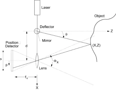
Optical triangulation and auto-synchronization have been described previously1. In a conventional triangulation-based range measurement system (Fig. 1), a light beam generated by a laser is deflected by a mirror and scanned on an object. A camera, consisting of a lens and position sensitive photodetector, measures the location of the image of the illuminated point on the object. The distance to the object can be computed using trigonometry and is directly related to the location of the point of illumination on the photodetector. As the light beam is scanned over the whole field, a trade-off arises between the field of view of the triangulation system, and the accuracy of the 3D measurement.
Figure 1: Basic principle of optical triangulation.
Synchronized scanner techniques extend the field of view of conventional triangulation-based methods. The basic idea is to use a scanning mirror to synchronize the projection of the light spot with its detection. The instantaneous field of view of the position sensor follows the spot as it scans the scene, without sacrificing accuracy.
Proc. SPIE Vol. 4661 11
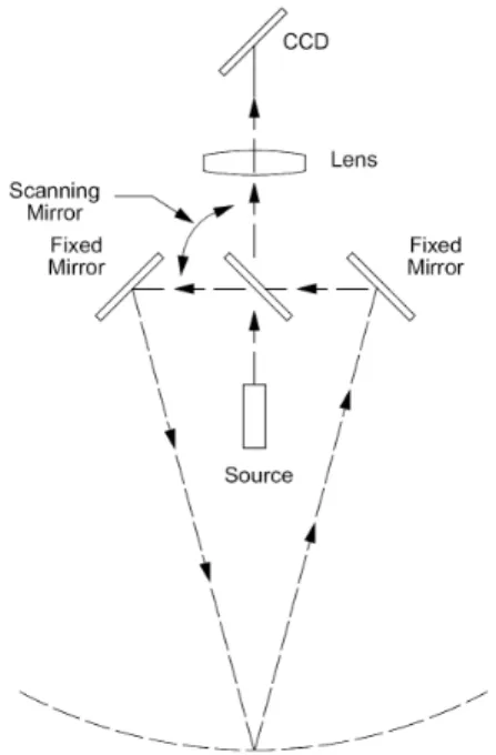
The optical configuration of an auto-synchronized scanner is illustrated in Fig. 2. While details of operation are beyond the scope of this paper, some aspects of the design will be briefly described. One side of a double-sided coated “scanning” mirror is used to deflect the laser beam. The other side collects the reflected light from the scene. This design offers some interesting advantages. For example, it reduces shadow effects due to the small separation between source and position sensor, and it offers improved immunity to ambient light and reflection because of the reduced instantaneous field of view. The configuration described here does not preclude a time-of-flight (LIDAR) mode of operation5.
Figure 2: Basic principle of the auto-synchronization method using a double-sided coated “scanning” mirror.
2.2 Applications of the LRSS
The LRSS has been implemented in a variety of different forms, each addressing a range of applications. Examples include7 CAD-based reproduction, heritage applications which includes the digitization of objects of historical significance, 3D anthropometry applications involving size and shape measurements of the human body, and space applications, such as the assembly and inspection of the International Space Station. Future applications of the LRSS foresee the development of a portable hand-held sensor that would simplify the task of documenting large, complex environments.
Our experience with these applications of the LRSS has made it very clear to us that the level of skill required at present, to produce high quality 3D imaging results is limiting the growth and acceptance of this technology. There is an obvious need to automate the configuration and control of the sensor system.
3. THE MDSP SYSTEM
3.1 Why DSPs?
A basic requirement of the system architecture being developed is that it must be able to address an ever changing and expanding research-oriented application. This places some interesting constraints on system design, perhaps the most challenging of which is the ability to expand the system in terms of both hardware (processors) and software (tasks). This is a principal design objective of MDSP.
Today, the clock rate of general-purpose processors (GPPs) used in desktop computers is reaching 2 GHz. The level of performance of these computers has reached the point where many applications that previously would never have been considered for a desktop machine can now be readily accommodated. On the other hand, DSPs have been announced offering significant performance-related features. For example, the TMS320C64xx™ now being developed by Texas Instruments is a fixed point DSP core that will eventually clock at speeds in excess of 1.1 GHz, will offer 32 DMA channels and a 2 level cache, including data cache. The selection of a processor must be based on a number of issues including power, cost, development tools, and performance-related features.
Power
Power is an important issue if portable systems are being considered. The TMS320C6201 requires about 5.5 Watts (typical)8 compared to 92.2 Watts (max)9 for a 1.8 GHz Pentium 4™.
Cost
For cost sensitive applications, DSP devices are significantly less expensive than GPPs. For example, at the time of writing, a 200 MHz TMS320C6201 costs about US$90. (in 40 unit quantities10) whereas a 1.8 GHz Pentium 4 was announced on July 2 2001 at US$562 (in 1000 unit quantities11).
Development Tools
Code generation and debugging tools have a major impact on the efficiency of the development effort. Unlike GPP tools, some DSP development tools implicitly support the debugging of multiprocessor systems and provide unique data visualization tools.
Processor Features
DSPs unlike GPPs are generally optimized for high throughput, data streaming applications. Some of the key features that support this include multiple bus architectures, multiple execution units that function in parallel, multiple data and instruction memories (both internal and external), multiple DMA channels for high speed data movement without processor involvement, special addressing modes such as circular or bit reversed addressing, and specialized instructions to handle saturation and normalization. Interrupt handling on DSPs is efficient and uncomplicated. Finally, some DSP families support high-speed interprocessor communications which can directly link together multiple DSP devices without any intervening logic.
The design of the LRSS requires the integration into a single system of a number of hardware components and one or more processors. The complexity of integrating external components with a processor is far higher for high performance GPPs than it is with low-end GPPs and DSPs12.
Real-time Constraints
Perhaps one of the most important aspects that underlies the design of the MDSP is the need to provide hard real-time performance. The LRSS is composed of two major units. The first is the range acquisition unit and the second is the optical deflection unit that provides the optical scanning. The degree of synchronization of these two components has a significant impact on the resulting accuracy of the LRSS. Any jitter that arises in this synchronization will lead to a degradation of LRSS accuracy.
While GPPs offer very high clock rates, their use of features such as branch prediction and speculative execution, features which do not appear on DSPs, can have a significant impact on run-time predictability which can lead to performance jitter13. If jitter is managed by conservative design practices based on worst case conditions, then performance will suffer.
Apart from the many innovative and powerful DSP devices that have become available over the past decade, commercial real-time operating systems (RTOS) have also appeared which support multiple DSPs. We have exploited these innovations in the design of the MDSP system.
Proc. SPIE Vol. 4661 13 3.2 Functional configuration of an experimental LRSS
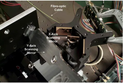
The prototype sensor head (Fig. 3) contains the electro-optical and electro-mechanical components. A fibre-optic cable carries the light from an external laser source to the sensor head. Two scanning mirrors, driven by galvanometers, provide the X-Y optical deflection for both the outgoing laser beam and the returning reflected light. A photodetector consisting of a 128-element CCD device is used for light capture.
Figure 3: The prototype sensor head. The double-sided X-axis scanning mirror is located slightly to the right of the center of the photograph. The CCD photodetector is mounted on a circuit board that is clamped to the back of the scanner frame. The large Y-axis scanning mirror is installed in front of the head.
The CCD device operates by discharging each CCD element at a rate that is proportional to the incident light intensity5.
At the conclusion of the integration period, the contents of all CCD elements are transferred in parallel to an internal register and shifted out in serial fashion. Clock generation hardware produces both the system clock used to drive the CCD device and the “VOXEL_CLOCK” which terminates the integration period and enables the internal data transfer. The CCD clock must be allowed to run continuously to avoid saturating the CCD device. Raw peak data generated by the CCD device is digitized by a 14-bit A-to-D converter producing a dynamic range of about 84 dB. The data are read directly by a DSP through a FIFO buffer.
Typically an LRSS is used in one of two modes: “imaging mode” whereby a complete image is digitized to completion, or “continuous mode” in which individual scan lines are produced continuously and the collected data are used immediately for real-time target acquisition and tracking purposes. Various scanning waveforms can be generated by an LRSS. A raster is used for image scanning whereas Lissajous patterns are used for tracking.
Operation of the prototype LRSS essentially involves slewing the deflection mirrors and then measuring, with sub-pixel accuracy, the corresponding position of the image peak on the CCD. The peak position and the intensity of the peak are then stored in a data buffer. The process is then repeated.
3.3 MDSP development sequence
The MDSP system was actually developed in two phases. We initially provided proof of concept using a mature generation of DSP devices, the TMS320C44 before proceeding with the design using a later generation of high performance DSPs, the TMS320C6x01. The following discussion focuses on the high performance implementation.
3.4 Modular computing hardware
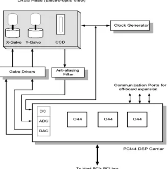
The sensor head of the LRSS was interfaced directly to the MDSP system. The initial system (Fig. 4) was built using a DSP "carrier" board manufactured by Innovative Integration Inc.14 This board is populated with three 50 MHz C44 DSPs and I/O hardware including off-board expansion. The high performance system (Fig. 5) used three DSP PCI boards, also manufactured by Innovative Integration Inc. The main board houses four, floating point 160 MHz C67 DSPs, all fully interconnected by high speed data links. Modularity is further supported by off-board data links for system expansion. The two M62 boards provide low-level I/O and dedicated front end processing.
Figure 4: MDSP “initial” system configuration showing the electro-optic view of the sensor head and the PCI44 DSP carrier board. The galvanometers are operated open-loop.
Figure 5: Processor configuration, modular high performance system. FIFOPorts interconnect the DSP boards while FIFOLinks (dashed lines) interconnect the C6701s on-board the Quatro67 card. All three boards reside on a host PC’s PCI bus.
Proc. SPIE Vol. 4661 15 3.5 Overview of modular software
System software was built using MQX™, a real-time multitasking operating system from Precise Software Technologies Inc.15 MQX supports modular design through implicit multiprocessing which means that tasks residing on different processors can communicate directly with one another. While task-to-task communication and synchronization is supported by a variety of mechanisms, message passing must be used when the tasks reside on different processors. A significant aspect of MQX is that the number of processors that can be combined into a single system is, for all practical purposes, limited only by hardware constraints. The addition or removal of processors is a simple process. An executable core image must be generated for each processor. Moving a task to a different processor or adding a task to a processor requires editing a task template list for those processors, and then rebuilding the core images.
MQX supports user defined interrupt handlers known as “notifiers”. A notifier is installed by an application task and is triggered by an internal or external interrupt. Once triggered, a notifier may signal a task and may also transfer interrupt-related data to that task. This provides a simple mechanism to synchronize runtime task behavior with internal or external events. A notifier is used by the MDSP to handle the CCD data traffic.
The initial system was implemented entirely with the multitasking abstraction of MQX. In the high performance system we found that in order to maximize performance, it was necessary to implement the CCD data peak detector and the low-level galvanometer control software as standalone components using dedicated processors without operating system support. These processors act in effect as specialized peripherals, receiving commands from the multiprocessor and returning data to it. All high-level functionality continued to be implemented using MQX.
Applications were written in C and were compiled using TI’s code generation tools. Hardware debugging support was provided by a JTAG debugger and Code Composer Studio10.
3.6 MDSP multiprocessor task configuration
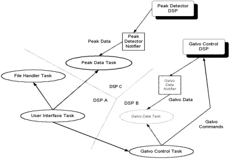
The task configuration is shown in Fig. 6. The multitasking abstraction that has been used provides a clear mechanism not only for expressing the software structure of the system but also for facilitating system expansion in the future.
Figure 6: MDSP Task Configuration for the Prototype LRSS. Five tasks, two notifiers and two standalone executables are implemented on five DSP devices.
The “User Interface Task” provides a simple menu interface to allow the user to set the LRSS scan parameters and to control its operation. The sensor can operate in either imaging mode where a complete scan is captured, or in continuous mode in which the sensor performs repeated scans. At the conclusion of an imaging mode scan, the data for an entire image can be written to a file on the PC.
The “Peak Data Task” is used to manage the acquisition of CCD position data (uncalibrated range data) and intensity data. After receiving a message from the User Interface Task, this task installs the “Peak Detector Notifier” that is triggered by the arrival of each new packet of CCD data. The notifier transfers the data to a data buffer managed by the Peak Data Task.
The “Galvo Control Task” is used to manage the operation of the scanning galvanometers. This task receives messages from the User Interface Task requesting that a scan be started, updated or terminated. The message that updates a scan contains a data structure that defines in detail the scan parameters for each scan axis.
The “File Handler Task” is used to support the creation of PC data files after an image is captured.
“Galvo Control” is an interrupt service routine that runs on a dedicated DSP. It receives commands from the Galvo Control Task via a high speed FIFOPort interface. In response to a VOXEL_CLOCK interrupt, it transfers the next X-axis and Y-X-axis waveform samples to the D-to-A converters that drive the galvanometers. It then computes the next sample values in preparation for the next interrupt and updates the synchronization signals.
“Peak Detector” has also been implemented as an interrupt service routine that runs on a dedicated DSP. It is triggered by the arrival of a new packet of raw CCD data. It computes the position of the peak (uncalibrated range) on the CCD detector to within a fraction of a pixel. It also determines the intensity of the peak. These data are then written to the FIFOPort for transfer to the Peak Data Task.
The Galvo Data Task and the Galvo Data Notifier have not yet been implemented. However they will provide similar functionality as the Peak Data Task and Peak Data Notifier but for galvanometer data.
Figure 7: An example of a range image captured by the LRSS. It combines range and intensity data and is presented here with synthetic shading.
The software described above consists of five tasks, two notifiers and two standalone executables which have been allocated to five DSP devices (Fig. 6). In the prototype system, we have measured the loading of the Peak Detector and Galvo Control DSPs to be 68% and 27% respectively. The four DSPs on the Quatro67 are essentially unloaded. They remain available for high-level processing such as real-time data calibration and post filtering, and geometrical object feature data extraction.
Proc. SPIE Vol. 4661 17 3.7 Example
An example of a scanned image generated by the LRSS is illustrated in Fig. 7. The object scanned was a plaster sculpture of a face of about 9 cm x 8 cm in dimension (H x W). The standoff distance for this scan was about 25 cm. In this figure, intensity and range data are combined and displayed as a synthetically shaded image. With the LRSS, range and image data are implicitly registered.
3.8 Performance
Performance of the LRSS is affected by a number of factors. These include the sensitivity of the CCD photodetector which influences the sensor’s integration time, the sample rate of the CCD, the bandwidth of the scanning galvanometers, the execution time of the peak detector and the rate at which data can be transferred through the system. In a high precision system such as this, it is very important to manage any jitter that may occur between the controlled scanning of the galvanometers and the sampling precision of the photodetector. The CCD sensor and the A/D converters are synchronized by a common hardware clock (Fig. 4). On the other hand, galvanometer waveforms are generated by interrupt-triggered DSP software and are issued, one sample at a time, to D/A converters. For a two-axis scanner, each interrupt results in the generation of a new pair of waveform samples. The relationship between the occurrence of a CCD range sample and the generation of the next galvanometer waveform sample is not exact. Despite the fact that both are ultimately based on a precise hardware clock signal, the waveform sample is actually software generated. This results in a minor variation or jitter between the two events.
We have measured the maximum waveform generation jitter of the C6x system to be in the order of ±220 ns. The prototype LRSS generates range samples at the rate of 39 kS/s. or every 25.6 µs. The jitter associated with the positional uncertainty is therefore ±0.22/25.6 or about ±1/116 of a voxel. This jitter is well below the system noise level and can be ignored. Jitter measurements of a GPP-based system have not been collected. It is expected that they would be significantly larger than the figures reported here.
4. RESULTS
An interesting aspect of this effort has been to be able to compare the performance of two generations of DSP devices for both peak detection and for interprocessor communications.
4.1 Peak detection - C44 vs. C6x
The accuracy of the LRSS is dependent upon the computed position of the laser spot on the photodetector that, after calibration, becomes the range sample. The algorithm used to perform peak detection16 uses FIR filters and linear interpolation to compute the peak position with sub-pixel resolution.
Earlier implementations of the LRSS used a combination of custom-built hardware digital filters and software interpolation to perform peak detection at high speed. Our measurements indicate that an all-DSP implementation using a 50 MHz C44 can accommodate a maximum CCD data rate of about 650 kHz, whereas a 200 MHz C6201 can achieve 6.7 MHz, which is about an order of magnitude faster.
For a 128 element CCD, a maximum CCD clock rate of 6.7 MHz corresponds to a range (voxel) sample rate of about 52 k samples/s, i.e. 52 kS/s. This includes the time required to transfer the contents of the CCD to the DSP and to perform the peak detection computation. In practice, we clock the CCD at 5 MHz which results in a 39 kS/s data rate.
4.2 Interprocessor communications (IPC) - C44 vs. C6x
The ability to pass messages of arbitrary length between tasks on different processors is of primary importance for MDSP. While message passing between tasks that reside on the same processor is implicit, transferring messages between tasks on different processors requires an interprocessor communications (IPC) mechanism. For the C44, this is provided at the chip level so C4x IPC remains the same regardless of the board being used. For the C6x family, IPC is a board-level design issue that must be ported to each hardware platform.
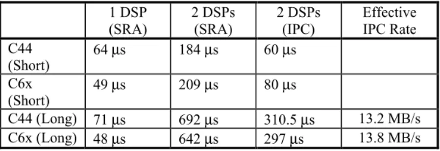
Measurements of IPC performance have been performed on both systems and will be briefly presented here. Representative tests were performed of message passing using short (24 byte) and long (4092 byte) messages on both C44 and C6x systems. A brief summary of the results is presented in Table I. Two tests were performed on each system using one processor, and two adjacent processors. In the single processor test, messages were sent between tasks on the same processor. This provides a baseline measurement of message-passing overhead without interprocessor communications.
Table I summarizes message passing performance using 50 MHz C44 DSPs and 160 MHz C6701 DSPs. The table lists the time required for a task to send a message and then to receive an acknowledgement message from a correspondent task. This is referred to in the table as a Send/Receive/Acknowledge (SRA) cycle and measures the end-to-end communication overhead. In the single processor case, message passing with the C6x simply passes pointers; data are not actually transferred. This is evident by the similar performance for the short and long messages (column 2). For the two processor case, the incremental cost of sending a message using the IPC is calculated by taking the difference between the two processor SRA cycle time and the single processor SRA cycle time and then dividing by two (column 4). The comparable performance of the two DSP devices (column 5), reflects the highly efficient design of the Comm Ports on the C44 and in particular, the use of level triggered interrupts17.
1 DSP (SRA) 2 DSPs (SRA) 2 DSPs (IPC) Effective IPC Rate C44 (Short) 64 µs 184 µs 60 µs C6x (Short) 49 µs 209 µs 80 µs C44 (Long) 71 µs 692 µs 310.5 µs 13.2 MB/s C6x (Long) 48 µs 642 µs 297 µs 13.8 MB/s
Table I: A Summary of Interprocessor Communication Performance for C44 and C6x DSPs.
Table II lists additional measurements which were obtained for simple, interprocessor message send and receive operations. The SRA times shown in Table I for the interlocked exchanges far exceed the send and receive times of Table II. SRA times measure the entire cost of an acknowledged message cycle whereas the send and receive times measure only the cost to each task of handling a message transfer. A large percentage of the time required to transfer a long message is actually spent in the DMA operations that occur largely in parallel with processor cycles. This is reflected by the relatively short time required by a task to send a message. The cost of message send and message receive operations on a single processor is shown for comparison. In this case, optimization is used to significantly reduce the message transfer times. Message length has no affect on performance for the single processor case.
Short Long Single Processor
Send 70 µs 121 µs 7 µs
Receive 3 µs 3 µs 4 µs
Table II: Performance of C6x for simple message send and receive operations for short (24 byte) and long (4092 byte) interprocessor and local message transfers.
5. CONCLUSIONS
In this paper we have described the design and preliminary results in the development of a modular DSP-based computing architecture for a real-time, high precision 3D laser range sensor system. We have described the motivation for the design which was to develop a high performance, modular architecture. Results obtained with the C6x system
Proc. SPIE Vol. 4661 19
indicate that significant gains in signal processing of about an order of magnitude can be achieved when compared with the earlier generation C44 system. However the performance of on-board interprocessor communications for message passing remains comparable to that obtained with the earlier C44 system.
Many of the advanced features now being considered for the next generation LRSS rely on high-level processing of the raw range data. The implementation of these features will rely heavily on the multiprocessor architecture.
Working demonstrations of the LRSS and of advanced waveform generation have been prepared. The application of this technology to target acquisition and tracking is now under consideration. Discussions are currently underway concerning the application of this architecture towards the development of an innovative portable hand-held LRSS.
REFERENCES
1. F. Blais, M. Rioux, and J.-A. Beraldin, “Practical considerations for a design of a high precision 3-D laser scanner system,” SPIE Proceedings, Vol. 959, pp. 225-246, June 28-29, 1988.
2. J.-A. Beraldin, S.F. El-Hakim, and L. Cournoyer, “Practical range camera calibration,” SPIE Proceedings, Videometrics II, Vol. 2067, pp. 21-31, Boston, MA, 1993.
3. F. Blais and J.-A. Beraldin, “Calibration of an Anamorphic Laser Based 3-D Range Sensor,” SPIE Proceedings, Videometrics V, Vol. 3174, pp. 113-122, San Diego, CA, 1997.
4. F. Blais, J.-A. Beraldin and S. El-Hakim, “Range error analysis of an integrated time-of-flight, triangulation, and photogrammetric 3D laser scanning system,” SPIE Proceedings, Laser Radar Technology and Applications V, Vol. 4035, pp. 236-247, Orlando, FL, 2000.
5. J.-A. Beraldin, F. Blais, M. Rioux, L. Cournoyer, D. Laurin, and S.G. MacLean, “Eye-safe digital 3D sensing for space applications,” Opt. Eng. 39(1), pp. 196-211, 2000.
6. F. Blais, R.A. Couvillon, M. Rioux, and S.G. MacLean, “Real-time tracking of objects for space applications using a laser range scanner,” Proceedings of the AAAI Conference on Intelligent Robots in Field, Factory, Service and Space, Vol. II, pp. 464-472, Houston, TX, 1994.
7. http://www.vit.iit.nrc.ca/VIT.html
8. “TMS320C6201, TMS320C6201B DIGITAL SIGNAL PROCESSORS SPRS051D – JANUARY 1997 – REVISED AUGUST 1998,” pp. 26, Texas Instruments Inc, 1998.
9. “Intel Pentium 4 Processor in the 423-pin Package at 1.30 GHz, 1.40 GHz, 1.50 GHz, 1.60 GHz, 1.70GHz, and 1.80 GHz,” Intel Document No. 249198-004, July 2001.
10. http://dspvillage.ti.com/
11. http://www.intel.com/pressroom/archive/releases/20010702comp.htm 12. http://www.bdti.com/articles/benchmark_000407.PDF
13. J. Eyre and J. Bier, “DSP Processors Hit the Mainstream,” IEEE Computer, 31(8), pp. 51-59, Aug. 1998. 14. http://www.innovative-dsp.com/
15. http://www.psti.com/
16. F. Blais, and M. Rioux, “Real-time numerical peak detector,” Signal Processing 11, pp. 145-155, 1986. 17. “TMS320C4x User’s Guide,” SPRU063B, Texas Instruments Inc. pp.11-42, 12-17, March 1996.