HAL Id: hal-03110777
https://hal-ifp.archives-ouvertes.fr/hal-03110777
Submitted on 14 Jan 2021HAL is a multi-disciplinary open access
archive for the deposit and dissemination of sci-entific research documents, whether they are pub-lished or not. The documents may come from teaching and research institutions in France or abroad, or from public or private research centers.
L’archive ouverte pluridisciplinaire HAL, est destinée au dépôt et à la diffusion de documents scientifiques de niveau recherche, publiés ou non, émanant des établissements d’enseignement et de recherche français ou étrangers, des laboratoires publics ou privés.
On the understanding of the optoelectronic properties of
S-doped MoO 3 and O-doped MoS 2 bulk systems: a
DFT perspective
Masoud Shahrokhi, Pascal Raybaud, Tangui Le Bahers
To cite this version:
Masoud Shahrokhi, Pascal Raybaud, Tangui Le Bahers. On the understanding of the optoelectronic properties of S-doped MoO 3 and O-doped MoS 2 bulk systems: a DFT perspective. Journal of Mate-rials Chemistry C, Royal Society of Chemistry, 2020, 8 (26), pp.9064-9074. �10.1039/D0TC02066D�. �hal-03110777�
1
On the understanding of the optoelectronic properties of S-doped
MoO
3and O-doped MoS
2bulk systems: A DFT Perspective
Masoud Shahrokhi
1, Pascal Raybaud
1,2*and Tangui Le Bahers
1*1Univ Lyon, ENS de Lyon, CNRS, Université Claude Bernard Lyon 1, Laboratoire de Chimie UMR 5182, F-69342 Lyon,
France
2IFP Energies nouvelles, Rond-point de l’échangeur de Solaize, BP 3, 69360 Solaize, France Authors for correspondence: pascal.raybaud@ifpen.fr; tangui.le_bahers@ens-lyon.fr
2
Abstract
First-principles calculations were carried out to understand the structure and optoelectronic properties of -MoO3 and 2H-MoS2 bulk systems with anionic isovalent-atom substitutions. The DFT
calculations have been performed by adopting HSE06 functional to probe the optoelectronic structures and Boltzmann transport theory to compute the DOS-averaged effective mass and mobility of studied compounds. Our first principle calculations indicate that substituting oxygen atoms by sulfur atoms on -MoO3, the electronic energy gap is decreased from 3.0 eV in pristine material to around 1.6 eV in
sulfur doped material. On the other hand, substituting sulfur atoms by oxygen atoms on 2H-MoS2 does
not produce significant change in the electronic band gap. We found that -MoO3 with high sulfur
concentrations (xs 33%) is thermodynamically stable and possess ideal dielectric function, optical,
charge transport and exciton binding energy for photocatalytic applications while for lower concentrations the carriers mobility is restricted due to the high value of carriers effective masses induced by localized electronic states. Probing the photocatalytic parameters for oxygen substituted 2H-MoS2 bulk system shows that this sulfide is not deeply altered by oxygen incorporation.
3
1. Introduction
In the quest for alternative approaches of producing clean fuels and chemicals, photocatalysis may represent an alternative and appealing pathway. However, one challenging bottleneck among others remains the improvement of the opto-electronic properties of the semi-conducting materials involved in the photocatalysts1. Photocatalytic activities are influenced by several properties of the
semiconductor, such as the electronic bandgap, the dielectric constant, the charge carrier effective masses, and the exciton binding energy. In a general view, a good photocatalyst should meet three requirements simultaneously: a suitable electronic band gap to efficiently absorb visible sunlight which is between 2.1 and 2.8 eV depending on the targeted applications (water splitting, CO2
reduction…),2 a dielectric constant greater than 10 to obtain optimal value of exciton binding energy
(Eb < 25 meV) and the carrier effective masses lower than 0.5 me in order to have a good mobility.3
While band-gap engineering is a rather well-established approach, the charge carrier dynamics including their generation and diffusion is less commonly and systematically determined whereas it remains crucial for photocatalytic properties enhancement. In the present report, we propose to address this challenging aspect for two families of semi-conducting materials potentially interesting for photocatalytic applications.
Molybdenum disulfide (MoS2) and molybdenum trioxide (MoO3) as layered materials with strong
intralayer iono-covalent bonding and weak van der Waals interlayer coupling, which gives the possibility to tune the number of stacked layers, garnered much research attention recently due to their rich physical and chemical properties beneficial for a wide range of applications4 and attractive for new domains of energies.5 Amongst the four various polymorphic phases of molybdenum trioxide [orthorhombic (-MoO3),monoclinic (-MoO3),hexagonal (h-MoO3),and high pressure monoclinic
(MoO3-II)] 6, -MoO3 with the orthorhombic layered crystal structure and Pnma space group is
thermodynamically most stable. -MoO3 is an n-type semiconductor with a wide experimental band
gap of ~3.2 eV 7,8. Due to its large band gap, -MoO
3 has applications in numerous optical and
electronic devices, including a transparent contact for organic photovoltaics or organic light-emitting diodes, photo- and electrochromic sensors, catalyst or gas sensor material and electrode material in
4
lithium batteries 9, 10, 11, 12, 13, 14, 15. Nevertheless, -MoO
3 can be activated under ultraviolet (UV)
irradiation (<387 nm) only, which represents about 5% of solar energy and is not optimal to be used as photocatalyst for solar-energy applications directly. On the other hand, molybdenum disulfide (MoS2) is a prototypical 2D layered transition metal dichalcogenide material that been studied
extensively over recent decades for its photoelectrochemical 16, catalyst 17,18, energy storage 19 and photovoltaic 20 properties. The thermodynamically stable phase of MoS
2 among its three phases (1T,
2H, and 3R 21, 22) is 2H phase with hexagonal crystal system and P6
3/mmc space group. In its bulk
form, 2H-MoS2 is a semiconductor with an indirect band gap of about 1.23 eV 23 and therefore it is not
a good candidate for photocatalysts. But, the combination of MoS2 and MoO3 materials can be found
in photoelectrocatalysis 24. The first reason of such combination is to build double-junction
photocatalysts in which the combination of a large and low bandgap materials can lead to an efficient water splitting catalyst. The other reason explaining the existence of such junction is the synthesis of MoS2 that can be done from MoO3 leading to a core MoO3 surrounded by MoS2 25. The diffusion of O
atoms from MoO3 to MoS2 and, reversely, the diffusion of S atoms from MoS2 to MoO3 can happen
during the lifetime of such a device involving a MoS2/MoO3 junction. Understanding the effect of this
phenomenon on the bulk properties of MoS2 and MoO3 materials seems an important topic of research
to understand the long-term stability of a device involving this junction. The second reason is that in the course of the synthesis of MoS2 phase from MoO3 precursors, the formation of Mo-oxysulfide may
take place which allows to tune the chemical composition of the materials 26. This investigation can
thus lead, as we will show later in text, to a proposition of new semiconductor composition.
Experimentally, Qin et al. showed that sulfur doping of molybdenum trioxide can improve the hole-transport properties of the host material27. Low concentration sulfur and selenium doping into α-MoO3
was theoretically found to be an efficient way to yield band gap reduction and the enhanced optical absorptions in the visible and infrared regions 28. However, it was shown that the low concentration level of S and Se-doping into -MoO3 could induce localized occupied states above the valence band
in the electronic band structure and restrict the free carrier mobility in these systems which are unfavorable to enhance the photocatalytic efficiency. Hence, it is important to investigate if it is
5
possible to tune the effect of dopant concentration on the localized/delocalized character of the dopant levels as a function of the dopant concentration in order to optimize the electronic properties of the material.
On the other hand, the effects of oxygen doping MoS2 nanosheets have received recent interest
because of its applications as electrocatalysts for hydrogen evolution reaction (HER). It appears that oxygen doping of MoS2 nanosheets reduces the energy barrier for H2 evolution and increases the
electric conductivity 29, 30, 31. Previous work has shown that creating molybdenum trioxide defects by oxygen plasma treatment in the MoS2 single-layer allows to tune the bandgap and control the optical
properties 32. Moreover, the band-gap of MoS
2 which is about 1.23 eV remains too small to make this
material valuable for photocatalytic applications. It thus appears relevant to explore if O doped MoS2
could help to improve the understanding of the increase of efficiency induced by such doping. Herein, we aim to address the opto-electronic properties of O-doped 2H-MoS2 and S-doped -MoO3
bulk systems in order to assess in one side the future potential of harnessing novel materials as a more efficient visible-light-driven photocatalysts and understand the effect of O doping in MoS2 or S doping
in MoO3 on the other side. As aforementioned, we will particularly pay attention to the charge
transport properties which are the most challenging aspects not so often addressed in the literature. The paper is organized as follows: in next section, the details of the computational methods employed to compute the crystal structure, electronic, charge transport and frequency depended optical properties are presented. Section 3 reports the results and discussion related to the structural properties of pristine and doped systems, the electronic and charge transport properties and the dielectric function and frequency dependent optical properties.
2. Computational Details
2.1 Total energy calculations
Total energy calculations including geometry optimizations of all structures were performed by periodic DFT using the PBE functional 33 and the Van der Waals contributions were described using
6
information) as implemented in the ab initio CRYSTAL17 code. 35 Localized Gaussian-type function
basis sets (BSs) were used: Mo_SC_HAYWSC-311(d31)G_cora_1997 36 (for Mo atoms),
S_86-311G*_lichanot_1993 37 (for S atoms) and O_8-411d11G_valenzano_2006 34 (for O atoms). All the
electronic properties were computed using single-point calculations by using the range separated hybrid Heyd-Scuseria-Ernzehof (HSE06) 39 exchange correlation functional on the PBE optimized geometries. Calculations of the electronic and ionic contribution to the dielectric constant were performed by using the PBE functional as implemented in CRYSTAL17. Infinite Coulomb and exchange sums are truncated according to following five thresholds 8 8 8 8 16 35. The convergence
criterion for the SCF cycle was fixed at 10-10 eV per unit-cell. Reciprocal space for unit-cell of MoS 2
and MoO3 containing 6 and 16 atoms, respectively, is sampled according to a sublattice with a
12128 and 81212 k-point mesh for geometry optimization, electronic band structure and Coupled Perturbed Kohn-Sham (CPKS) 40 calculations. The k-point mesh sampling is progressively reduced as the size of the semiconductor unit cells increases for doped materials (see Table S1 and Table S2). To identify the most stable MoO S and MoS O compositions as a function of the number of S- or O-atoms exchanged in the MoO and MoS structures respectively, we calculate the Grand potential, Ω, assuming that the reservoir surrounding the solids is constituted from ideal gas phase mixtures of H2S/H2O (commonly used experimentally as sulfiding and oxidizing agents) :
MoO3 + xH2S = MoO(3-x)Sx + xH2O (1)
MoS2 + xH2O = MoS(2-x)Ox + xH2S (2)
Ω E MoO S E MoO xG, H O xG, H S xRT ln (3)
Ω E MoS O E MoS xG, H S xG, H O xRT ln (4)
where E stands for the 0 K, formation energies of the different solids involved (neglecting vibrational and entropic contributions, see also supporting information), G, stands for the Gibbs free energies of formation of H2S and H2O molecules (including thermal and entropic effects evaluated from NIST
data base at T0=298 K). So, for each value of x, we will plot the evolution of Ω as a function of the
7
K.
Note that increasing T slightly diminishes the free enthalpy of oxidation reaction of MoS
2while slightly increases the free enthalpy of sulfidation of MoO
3(see supplementary
information). However, the main trends reported at ambient T are only very weakly affected.
2.2 Transport properties
To quantify the carriers mobility, we computed the effectives masses (me* and mh*) from two
approaches: by fitting the bands with a parabolic function and by integrating the DOS. In the first model the electron and hole effective masses in various crystallographic directions can be calculated according to its band structure curvature at the extrema points 3 according to this formula:
E ⁄ k⃗ E ℏ ∗ k k
ℏ
∗ k k
ℏ
∗ k k (5)
where ECB/VB is the conduction and valance bands eigenvalues, Emin is the energy at the extrema point, k are the k-space reciprocal lattice points, mx*, my* and mz* are the effective masses along x, y and z directions, and ki-min is the band edge position in reciprocal space. The parabolic model has two main limitations: (i) the vicinity in energy of other band extrema and (ii) the adversity of an appropriate choice of crystallographic directions, therefore it cannot properly delineate effective masses 2. The
DOS-averaged effective mass using the semi-classical Boltzmann theory is the second approach adopted in this work which go beyond these limitations. The evaluation of the electronic transport properties was performed departing from the PBE-optimized geometry via single-point HSE06 calculations within the Boltzmann transport equation (BTE) involving a constant scattering time ( = 10 fs) as implemented within CRYSTAL17 41, 42. For these properties we used a k-point mesh sampling at least 2 times denser than what we employed for geometry optimization in each structure.
2.3 Optical properties
The optical properties were calculated through the frequency-dependent dielectric matrix 𝜀 𝜔 , by using the Vienna ab initio Simulation Package (VASP)43,44 and the methodology described in Ref. 45
and successfully applied to N- and S-doped TiO2 materials 46,46,47. For that purpose, we used the
(HSE06) 39 exchange correlation functional a kinetic energy cut-off of 500 eV for the plane wave basis
8
structures obtained previously with CRYSTAL were used. The number of empty conduction bands (NBANDS) was converged for each structure with respect to standard calculations.
The absorption coefficient is calculated by using the following relationship:
α ω (6)
where c is the speed of light in vacuum. nαβ and kαβ are real and imaginary parts of the complex refractive index, and are known as the refractive index and the extinction index, respectively. They are given by the following relations:
n ω | | (7) k ω | | (8)
2.4 Exciton binding energy
The relative dielectric permittivity (r) or more generally called relative dielectric constant results from
the contribution of the electron density () and of the ion vibrations (vib):
ε ε ε (9)
The exciton binding energy (Eb) values for these structures are calculated in the framework of the
Mott-Wannier model 48.
E E m∗
ε 10
where EH is the energy of the 1s orbital of hydrogen (−13.6 eV) and mr* is the reduced mass of the
exciton:
∗ ∗ ∗ (11)
3.
Results3.1 Energetic stability and structural properties
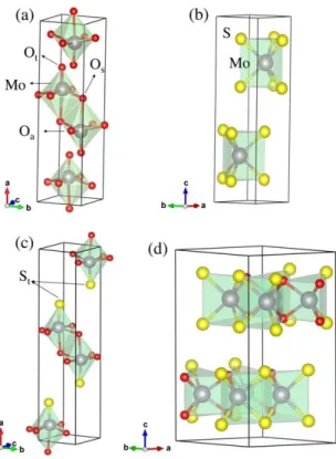
In the crystal structure of -MoO3 (Fig.1 (a)), where Mo atoms are an octahedral environment
surrounded by 1 O-oxo species and 5 bridging O atoms. In 2H-MoS2 (Fig.1 b), each Mo atom is in a
trigonal prismatic environment surrounded by 6 S atoms shared themselves by 3 Mo atoms. To study the effects of sulfur doped -MoO3 and oxygen doped 2H-MoS2 structures, different dopant
9
to 33% and O-substituted MoS2 bulk with O concentration up to 75%. For high concentration of
dopant, the stability of the native structure is suspected to be questioned. As detailed in supplementary information, we will consider that the complete MoO3/MoS2 inter-conversion can be prevented under
controlled H2S/H2O environment. On the one hand, the oxidation of MoS2 into MoO3 is an
endothermic process in H2S/H2O (this is not the case in O2/SO2 environment, as exemplified in
supplementary information). On the other hand, the full sulfidation of MoO3 into MoS2 in H2S/H2O
would require the presence of H2. Furthermore, the 33% of S doping in MoO3 corresponds to all
oxo-terminal positions substituted by S (as discussed later in the text) keeping the internal cohesion of MoO3 layers intact. Higher S-doping concentration would require substituting large concentration of
bridging oxo, inducing the reconstruction of the native MoO3 into more complex oxisulfides
(amorphous) as suggested by experimental observations 49,50,51. Such an investigation is beyond the
scope of the present study.
For each doping level, several configurations were tested and only the properties of the most stable ones are presented in the text. Fig. 1 c and d illustrate two examples, for more information see the supporting information SI 2. Table S1 and S2 report the optimized lattice parameters and formation energies (Ef) of all studied S-substituted -MoO3 and O-substituted 2H-MoS2 bulk systems,
respectively. By increasing sulfur concentration, the MoO3 lattice parameter (a) perpendicular to the
basal plane of the layer increases while the in-plane lattice parameters (b and c) remain almost unchanged. In contrast, by increasing the O concentration in MoS2, the c-parameter remains almost
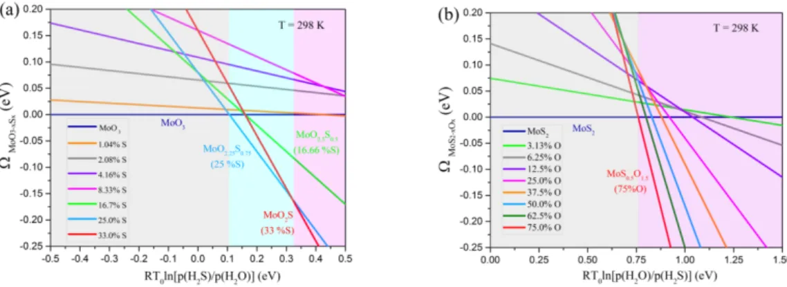
constant up to 50% O substitution. In order to discern on structural stability of these systems in more realistic conditions, we determine the thermodynamic phase diagrams (Fig. 2) of substituted systems with respect to the pristine structures by using the Grand potential approach. By using H2O as oxygen
source and H2S as product (as used experimentally, see also Methods), the calculated reaction energies
reveal that MoS2 bulk oxidation is difficult particularly at high concentration (Figure S9). By contrast,
the sulfidation of MoO3 by H2S is less difficult specially for S concentration higher than 17%. Fig. 2
(a) indicates that for a RT ln term greater than ~0.1 eV which corresponds to ~50, the
10
with 25% S is the most stable. For RT ln higher than 0.32 eV, system with 33% S is thermodynamically favored. By contrast, Fig. 2 (b) shows that the oxidation of MoS2 requires value of
RT ln as high as 0.75 eV corresponding to ~10 , which implies that the MoS2 pristine
system should remain stable while the structure with the highest O concentration (the one tested here at 0.75%) should be favored. However, we cannot exclude that different oxidizing agents or reaction pathways may be used to make the oxidation process thermodynamically favorable. For instance, by using O2 as oxidizer and SO2 as a byproduct, it can be shown that reaction energies become
exothermic and the thermodynamic diagram can be shifted to accessible reaction conditions (see Figure S10).
Fig. 1. The unit-cells of (a) -MoO3 (including 4 Mo and 12 O atoms), (b) 2H-MoS2 (including 2 Mo and 4 S atoms) (c) -MoO2S(including 4 Mo, 8 O and 4 S) and (d) 2H-MoSO (including 8 Mo, 8 S and 8 O) structures. The three
inequivalent oxygen atoms in -MoO3 structure are labeled: Ot is the apical oxygen atoms, Oa is the corner-sharing
oxygen atoms and Os is the edge-sharing oxygen atoms. While all S atoms in MoS2 structure are equivalent. The
11
Fig. 2 Thermodynamic phase stability of the S-substituted -MoO3 (a) and O-substituted 2H-MoS2 (b) bulk structures
for different S- and O-concentrations with respect to pristine structures considering H2S/H2O reservoir
In term of bonding nature, the partial charge (Bader charge 52) of S atoms in doped MoO3 in absolute
value is smaller than the one of oxygen atoms (∼0.25 for S vs ∼0.8 for O) highlighting the less ionic character of the Mo-S bond than the Mo-O bond, in agreement with the lower electronegativity of S versus O. The less ionic (and thus more covalent) character of the Mo-S bond than the Mo-O bond is also observed in O doped MoS2 systems. This is further confirmed by the analysis of the redistribution
of electron density in those systems (see Supporting Information Figure S11).
3.2 Electronic structure and absorption coefficient
To probe the electronic properties of S-doped -MoO3 and O-doped 2H-MoS2, the band structures and
the partial density of states (PDOS) of these systems have been calculated. Fig. 3 shows the band structure along the high symmetry directions and the projected density of states (PDOS) of pristine -MoO3 and 2H-MoS2 structures and two relevant substituted systems for S-substituted -MoO3 with
the concentration of 33% and O-substituted 2H-MoS2 with the concentration of 50.0% obtained with
HSE06. Both MoO3 and MoS2 exhibit an indirect bandgap with a computed value of 2.96 eV and 1.56
eV respectively, thus close to the reported experimental values of 3.0-3.2 eV 7,8 and 1.2-1.3 eV 53,54
respectively. A better agreement between theory and experiment could be possible by using a global hybrid functional involving a tuned exact exchange fraction (i.e. exact exchange equal to 1/) with
the positive point to give faster calculation than with the range separated hybrid functional HSE06 but with the main drawback to change the functional for any material 55,56,1. In our work, we decided to
12
keep the same functional, HSE06, for all calculation even if a slight discrepancy between theory and experiment exists. The PDOS of -MoO3 bulk shows the top of the valence band (VB) is dominated
by O 2p orbitals (Fig. 3 a), whereas the bottom of the conduction band (CB) is formed from Mo 4d orbitals with weak hybridization of O 2p states allowing us to conclude on the charge-transfer insulator character of this material. On the opposite, the PDOS of 2H-MoS2 bulk indicates that both
the top of the valence band and the bottom of the conduction band are dominated by Mo 4d orbitals with weak hybridization of S 3p states resulting in Mott insulator. This PDOS feature is induced by the trigonal prismatic environment of Mo atoms leading to the splitting of their 4d states into a1g
orbital located at the top of VB and eg states at the bottom of CB. 57
Upon substitution of O atoms by S atoms in -MoO3, a significant decrease of the energy gap is
computed with values ranging from 1.61 eV to 1.87 eV depending on sulfur concentration (Fig. 4 (a) and Table S3) while keeping the indirect nature of the band gap. The abrupt band gap decreases induced even by the minimum sulfur doping considered originates from the appearance of sulfur state inside the MoO3 pristine bandgap. In the Figure S12 in SI illustrates band structure and PDOS of the
most stable S-substituted -MoO3 bulk structures. We found that at low sulfur concentration, the
impurity bands are localized and situated above the VB maximum (in the band gap) of -MoO3. These
impurity states originate from the 3p orbitals of S atom and restrict the free charge carrier mobility as it will be further discussed for concentration lower than 8.3%. For higher S-concentrations, such as 33% S (Fig. 3 c), the 3p orbitals of S atom are located at the top of the VB and starts to mix with the Mo 4d orbitals which may have positive effects on the mobility.
For O-doped MoS2, it is found that substituting sulfur atoms with oxygen atoms for all concentrations
does not produce significant change in band gap (Fig. 4 (b) and Table S4). Figure S16 illustrates band structures and PDOS and Table S4 summarized the optoelectronic properties of the most stable O-substituted 2H-MoS2 bulk structures.
The fluctuation observed in the bandgap for large doping concentration for both MoS2 and MoO3
based materials probably originates from the choice to present only the most stable solid solution for each concentration. But even if there are some fluctuations in the bandgap, these variations remain in
13
the standard deviation of HSE06 (
around 12%)
58,3 allowing us to conclude that the doping, at the concentrations considered, as a weak effect on MoO3 and MoS2 in term of bandgap.Fig. 3. Band structures and PDOS of -MoO3 (a), 2H-MoS2 (b), -MoO2S(33%) (c) and 2H-MoSO (50%) (d) at
14
Fig. 4. Computed electronic band gaps (in eV) and absorption coefficient (, in cm-1) of the most stable S-substituted -MoO3 (a and c) and O-substituted 2H-MoS2 (b and d) bulk structures for different S- and O-concentrations within
HSE06.
The calculated absorption coefficients for pristine and doped systems (Fig. 4 and Fig. S18) show both highly anisotropic optical properties in these systems but with distinct anisotropic behaviors: the in-plane (within the layer) absorption coefficient in MoS2 is larger than the absorption coefficient out of
plane (in the interlayer direction) whereas the out-of-plane (perpendicular) is predominant in MoO3
based materials (Fig. S18). However, the electronic band gaps for both substituted systems were found to be in the same range but the absorption spectra dramatically change by increasing the concentration of doping impurities. These results show that by enhancing S concentration the absorption coefficient of MoO3 system is increased in the UV−vis window while it is reduced by increasing the O fraction on
15
MoS2 system. For S-doped MoO3, a strong increase of absorption coefficient is observed for
S-concentration greater or equal to 16.7%, which makes this system interesting with that respect.
In general, despite the indirect band gap nature of S-doped MoO3 and O-doped MoS2 systems, the
high absorption coefficients were attained (~105 cm−1) for all structures except pristine -MoO
3: this is
higher than the typical absorption coefficient value for direct band gap semiconductors across the entire UV−vis range 59.
3.3 Charge transport
The charge carrier effective mass for -MoO3 along [100] (i.e. interlayer) direction are very large due
to the dominance of Van der Waals (vdW) interactions between the layers in -MoO3 systems. The
mobility of charge carriers in this interlayer direction is probably more governed by a polaronic model than a rigid band model assumed in the effective mass analysis. Thus, in the parabolic model for MoO3, we only considered an average value which do not include [100] direction to calculate carriers
effective mass. Table S3 listed the harmonic average of electron and hole effective masses for S-substituted -MoO3 systems along [010], [001] and [011] directions. The electron and hole effective
masses for pristine -MoO3 bulk within the parabolic model are respectively 0.63 and 0.40 me, in a
good agreement with previous theoretical data 60. The electron effective mass obtained this method is
slightly increased by increasing sulfur concentration while the hole effective mass is decreased. Table S3 also compares the effective mass of electron and hole obtained from DOS-averaged approach for S-substituted -MoO3 bulk system and the Boltzmann transport results are presented in Fig. S19. The
electron and hole effective masses for pristine -MoO3 bulk within the DOS-averaged model are
respectively 0.61 and 1.13 me leading to the mobility of 29 and 16 cm2V-1s-1 for electrons and holes,
respectively. As it can be seen from Fig. 5 and Table S3 the DOS-averaged electron effective masses for xS = 1.04%, 2.08% and 4.16% are 3.78, 2.80 and 2.31 me resulting in mobilities of 5, 6 and 8
cm2V-1s-1, respectively, which are significantly smaller than the electron mobility for pristine -MoO 3.
The corresponding hole effective mass values for the same concentrations are 4.75, 5.6 and 1.74 leading the hole mobility of 4, 3 and 10 cm2V-1s-1. For higher concentration levels (xS 16.7%), as
16
of O atoms and 4d of Mo atoms nearby which eliminates localized impurity bands and increases carrier mobility. It is unveiled that due to the light DOS-averaged electron effective masses for xs >
16.7%, the average electron mobility of these compounds is predicted to be reasonably high (especially for xS=16.7% and xS=33%). In general, for high sulfur concentrations, electrons were
found to be more mobile than holes in S-doped -MoO3 systems. Moreover, for xS 16.7% the order
of magnitude of charge carrier mobilities agrees well with the good charge collection efficiency. Our results indicate that the carriers effective mass for MoS2 compounds along the vdW interlayer
direction are in the order of those along in-plane directions, hence all in-plane and out-of-plane directions have been taken into account to calculate carriers effective masses in parabolic model. The electron and hole effective masses obtained from parabolic model are 0.82 m0 and 0.67 m0 (Table S4),
in a good agreement with previous work (me* = 0.821 m0 and mh* = 0.625 m0) 61. The corresponding
values for me* and mh* within DOS-averaged model are 0.38 m0 and 0.23 m0. The light electron and
hole effective masses of pristine 2H-MoS2 bulk lead to a desirable high electron and hole mobility (e
= 46 cm2 V-1s-1 and
h =75 cm2 V-1s-1). From Fig. 5 and Table S4 it can be seen that by increasing
substituting sulfur atoms with oxygen, the electron and hole effective masses are increased resulting in carriers mobility reduction. Nevertheless, the orders of magnitude of electron and hole mobilities for both pristine and O-doped systems agree well with a good charge collection efficiency. Among all these systems, MoSO structure (xO = 50.0%) with wide band gap of 1.71 eV and high carrier mobility
17
Fig. 5 Electron and hole mobility (in Cm2V-1s-1) of the most stable S-substituted -MoO
3 (a) and O-substituted
2H-MoS2 (b) bulk structures for different S- and O-concentrations within HSE06.
3.4 Dielectric constant
As presented in the Introduction, a high relative dielectric constant (r) correlates with a low binding
energy (Eb) is necessary to dissociate the excitons into free charge carriers in semiconductors 3. Tables
S5 and S6 and Fig. 6 summarizes the calculated the electronic and relative dielectric constant ( and
r) and exciton binding energy (Eb) of the most stable S-substituted -MoO3 bulk and O-substituted
2H-MoS2 bulk structures. Both electronic contribution () andionic vibrational contribution (vib) for
pristine bulk structures along the interlayer direction are smaller than those along in-plane directions. The geometric average of for pristine -MoO3 (5.6) is lower than 2H-MoS2 (11.0) because of two
correlated effects: sulfur is more polarizable than O and the S bond is more covalent than the Mo-O bond, as discussed before. In contrast, the large vib computed in -MoO3 compared to MoS2 bulk,
comes from the larger ionic character of oxides than sulfides 32. Furthermore, by increasing S
concentration in both systems, increases mainly because sulfur atoms are more polarizable than
oxygen atoms as said previously 62, 63. By increasing sulfur concentration in -MoO
3 structure, r is
enhanced from 13.9 for xS =0.0% to 17.9 for xS =33.0% thus within the range that is required for solar
energy conversion (r > 10) 3
18
concentration from 11.1 for pristine structure to 8.9 for xO = 75% that is reasonably high to consider
these materials for photocatalytic application3.
The exciton binding energy for pristine -MoO3 bulk (28 meV) increases for low sulfur doping
concentrations (xS 8.3%) due to the high value of mr* itself induced by the localized electronic states
of the dopant. For high sulfur concentration levels (xS 17%) the Eb significantly decreases because of
high relative dielectric constant and low values for reduced effective masses. Especially for xS = 17%
and 33% the Eb is slightly lower than the determined threshold needed for charge carrier separation by
thermal energy (25 meV at room temperature) together with low effective masses and large dielectric constant resulting in enhancement of the excitons dissociation efficiency.
The exciton binding energy of pristine 2H-MoS2 is 16 meV, and in a good agreement with previous
results (~20 meV) 64. By increasing the O-doped concentration level into 2H-MoS
2 bulk the Eb is
slightly increased for concentrations lower than 25% while it experiences a sharp increase for higher concentrations (xO 37.5%). These results confirm that the oxygen content of MoS2 must be kept as
19
Fig. 6. Computed electronic dielectric constant (), relative dielectric constant (r) and exciton binding energy (in
meV) of the most stable S-substituted -MoO3 and O-substituted 2H-MoS2 bulk structures for different
concentrations.
4.
ConclusionsIn summary, we performed a detailed first-principles calculation to study the structural, electronic, charge transport and optical properties of sulfur doped α-MoO3 and oxygen doped MoS2 bulk systems.
In order to compare the stability of the various MoO S structures in H2S/H2O environment which
may be relevant for water splitting or CO2 reduction, the phase diagram analysis revealed that MoO3
with 25% and 33% S-(such as MoO2S) concentrations can be thermodynamically stabilized under
reasonable ratio. However, it appears that it is far more difficult to oxidize MoS2 into
MoS O by using H2O/H2S environment, whereas it can become thermodynamically accessible by
20
Regarding opto-electronic properties, Table 1 summarizes the key calculated parameters of pristine -MoO3 and 2H-MoS2 bulk systems with two relevant substituted structures (MoO2S and MoSO).
MoO3 MoO2S MoS2 MoSO
Eg (eV) 2.96 1.80 1.56 1.71 me*a (me) 0.63 0.68 0.82 0.40 mh*a (me) 0.40 0.11 0.67 0.59 me *DOSb(me) 0.61 0.48 0.38 0.40 mh *DOSb(me) 1.13 1.77 0.23 0.86 μe c (cm2V-1s-1) 29 37 46 44 μh c (cm2V-1s-1) 16 10 75 20 5.6 8.20 11.0 8.8 r 13.9 17.90 11.1 9.1 Eb (meV) 28 16 16 44
Table 1. DFT calculated band gap energy, effective mass of electron and hole, DOS- averaged effective masses, electron and hole mobility, electronic dielectric constant (), relative dielectric constant (r) and exciton binding
energy (Eb) of -MoO3, MoO2S, 2H-MoS2 and MoSO systems. aHarmonic average of different directions (see Table S3
and S4 for more information). b DOS- averaged effective masses and mobility obtained from the Boltzmann transport
theory as implemented in CRYSTAL17 code and calculated at a carrier density of 1017 cm-3. c The mobility was
estimated under the assumption of = 10 fs.
Both MoO3 and MoS2 were confirmed to be indirect bandgap semiconductors with a 2.96 eV and 1.56
eV gap, respectively, by using the HSE06 functional in agreement with experimental data. As reported in Table 1 for the MoSO case (50% O), substituting sulfur atoms by oxygen atoms on 2H-MoS2 does
not produce significant change in the electronic band gap which may remain too low (Eg = 1.5-1.7 eV)
for many applications (CO2 reduction or H2O splitting). Nevertheless, the oxygen substituted
2H-MoS2 bulk systems with O-concentration up to 50% possess interesting properties: r ~ 8, > 105
cm−1 and E
21
contrast, substituting the Ot sites in -MoO3 by sulfur atoms may significantly impact the electronic
energy gap which decreases from ~3.0 eV in pristine material to around 1.6 eV in sulfur doped material. To avoid localized impurity states, our study suggests to use -MoO3 with sulfur
concentrations higher than 17% possess good optical properties (Table 1): electronic band gap (~ 1.80 eV), dielectric function (r > 17), optical absorption ( > 105 cm−1). Regarding charge mobility (μe=37,
μh=10) and exciton binding energy (Eb ~ 16 meV), they are compatible with various photocatalytic
applications. In order to attempt to further optimize the two MoO3 and MoS2 layered materials, we
propose in future works to address how the calculated optical properties can be tuned by decreasing the number of stacked MoO3 or MoS2 layers, assumed to be infinite in the present work devoted to
22
Acknowledgements:This work is part of the “RatiOnAl Design for CATalysis” (ROAD4CAT) industrial chair, project IDEXLYON funded by the French National Research Agency (ANR-16-IDEX-0005) and the Commissariat-General for Investment (CGI) within the framework of Investissements d’Avenir program (“Investment for the future”). The authors thank the SYSPROD project and AXELERA Pôle de Compétitivité for financial support (PSMN Data Center). This work was granted access to the HPC resources of CINES, IDRIS and TGCC under the allocation 2018-080609 made by GENCI.
Supporting Information:
The supporting information contains the optimization of D3 correction parameters for MoS2 and
MoO3; the details of the thermodynamic analysis; the bond nature analysis; the details of the