https://doi.org/10.4224/9184141
READ THESE TERMS AND CONDITIONS CAREFULLY BEFORE USING THIS WEBSITE.
https://nrc-publications.canada.ca/eng/copyright
Vous avez des questions? Nous pouvons vous aider. Pour communiquer directement avec un auteur, consultez la première page de la revue dans laquelle son article a été publié afin de trouver ses coordonnées. Si vous n’arrivez pas à les repérer, communiquez avec nous à [email protected].
Questions? Contact the NRC Publications Archive team at
[email protected]. If you wish to email the authors directly, please see the first page of the publication for their contact information.
NRC Publications Archive
Archives des publications du CNRC
For the publisher’s version, please access the DOI link below./ Pour consulter la version de l’éditeur, utilisez le lien DOI ci-dessous.
Access and use of this website and the material on it are subject to the Terms and Conditions set forth at
Smart sensors for 3D digitization
Gonzo, L.; Gottardi, M.; Comper, F.; Simoni, A.; Beraldin, Jean-Angelo
(Angelo); Blais, F.; Rioux, M.; Domey, J.
https://publications-cnrc.canada.ca/fra/droits
L’accès à ce site Web et l’utilisation de son contenu sont assujettis aux conditions présentées dans le site LISEZ CES CONDITIONS ATTENTIVEMENT AVANT D’UTILISER CE SITE WEB.
NRC Publications Record / Notice d'Archives des publications de CNRC:
https://nrc-publications.canada.ca/eng/view/object/?id=86c30536-554a-4dbf-a8dd-12a9714b81d1 https://publications-cnrc.canada.ca/fra/voir/objet/?id=86c30536-554a-4dbf-a8dd-12a9714b81d1
National Research Council Canada Institute for Information Technology Conseil national de recherches Canada Institut de Technologie de l’information
Smart Sensors for 3D Digitization*
Gonzo, L., Gottardi, M., Comper, F., Simoni, A.,
Beraldin, J.-A., Blaid, F., Rioux, M., and Domey, J.
April 2001
Copyright 2001 by
National Research Council of Canada
Permission is granted to quote short excerpts and to reproduce figures and tables from this report, provided that the source of such material is fully acknowledged.
*
published in Proceedings of the Workshop 2001 Italy-Canada on 3D Digital Imaging and Modeling Application of: heritage, industry, medicine, and land. Padova, Italy. April 3–4, 2001. NRC 44156.Smart Sensors for 3D Digitization
L. Gonzo, M. Gottardi, F. Comper and A. Simoni ITC-Istituto per la Ricerca Scientifica e Tecnologica
via Sommarive 16, I-38050 Povo, Trento, Italy
Email: [email protected]
URL: http://www.itc.it/irst/attivita/integrazione.html
J-Angelo Beraldin, F. Blais, M. Rioux and J. Domey National Research Council Canada, Institute for Information
Technology Ottawa, Canada, K1A 0R6 Email: [email protected]
URL: http://www.vit.iit.nrc.ca
KEY WORDS: 3D vision, laser spot position sensors, opto-sensors
ABSTRACT
This paper presents our activities on smart VLSI opto-sensors for 3D vision. A description of the integrated devices jointly devel-oped for industrial and scientific applications will be given. All the sensors presented here have been fabricated using standard CMOS technology that allows the monolithic integration of photo-sensors, together with readout circuits, and digital signal proces-sors.
INTRODUCTION
Digital 3D imaging can benefit from advances in VLSI technology in order to accelerate its deployment in many fields like visual communication and industrial automation. The NRC and IRST groups are collaborating on a project that is tar-geted at the integration of key sensors. These sensors include the synchronization photodiodes based on integrated bi-cells [1] and the laser spot position measurement sensors [2]. These sensors could become an integral part of future intelligent digitizers that will be capable of measuring accurately and simultaneously colour (reflectance) and 3D. This, in turns, will accelerate the development of hand-held 3D cameras [3], and, multi-resolution random access laser scanners for fast search and tracking of 3D features [2]. All these digitizers will require a thorough VLSI integration of basic laser camera func-tions to achieve size and cost reduction and most importantly, higher performance.
COLOUR 3D IMAGING TECHNOLOGY
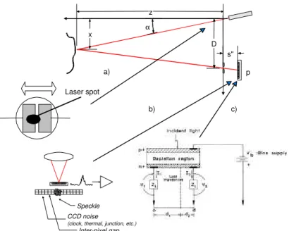
Machine vision involves the analysis of the properties of the luminous flux reflected or radiated by objects. To recover the geometrical structures of these objects, either to recognise or to measure their dimension, two basic vision strategies are available. The first strategy, known as passive vision, attempts to analyse the structure of the scene under ambient light. In contrast, the second, known as active vision attempts to reduce the ambiguity of scene analysis by structuring the way in which images are formed. By keeping the properties of invariance in rotation and translation of 3D objects, sensors that capitalize on active vision can resolve most of the ambiguities found with 2-D imaging systems. Moreover, with laser-based approaches, the 3D information becomes relatively insensitive to background illumination and surface texture. Com-plete images of visible surfaces that are rather featureless to the human eye or a video camera can be generated. Thus, the task of processing the 3D data is greatly simplified. Lidar-based or triangulation-based laser range cameras are examples of vision systems built around such strategy [4]. Active triangulation is used in applications as diverse as reverse engineering, wood measurement, 3D documentation of cultural heritage sites [5], inspection of printed circuit boards, and automatic ro-bot welding. Two digital 3D imaging systems were developed and demonstrated at the National Research Council of Can-ada (NRC). They are the auto-synchronized principle [6] and the BIRIS [7] system. These range cameras provide registered range and intensity data for visible surfaces (either monochrome or colour). Figure 1 depicts the optical geometry of a range based on triangulation along with some of its position sensors. A 3D surface map is captured by scanning a laser spot onto a scene, collecting the reflected laser light from a different vantage point (triangulation), and finally focusing the beam onto a position detector. A similar geometry can be based upon the projection of a laser line instead of a single laser spot.
Geometric correction of the raw data gives two images in perfect registration: one with x, y, z co-ordinates and a second with intensity data representing the collected laser power from the scene. The laser beam can be of a single wavelength (visible or infrared) or composed of multiple visible wavelengths for the purpose of measuring the colour map of a scene (reflectance map).
LASER SENSORS FOR 3D IMAGING
It is within the scope of this project that collaboration between the two groups was initiated. The result of this work has provided unique sensors that will allow 3D digital imaging technology to face the challenge posed by the many emerging markets. This research and development work will also contribute to the advancement of knowledge in 3D digital imaging. The following sensors are targeted for integration into VLSI:
A) Synchronization circuit based upon dual photocells (bi-cell) --> This sensor ensures the stability and the repeatability of
range measurements in environment with varying temperature. Discrete implementations of the so-called synchronization circuits have posed many problems in the past. A monolithic version of an improved circuit (smart) has been built to allevi-ate those problems [1].
B) Smart 3D position sensors --> Integration of most low level processing steps on a chip using advances in VLSI will
al-low digital 3D imaging technology to become widely accepted and accessible to research labs, universities, industries, hob-byists, and, also to the home. Currently, commercial photodiode arrays used in 3D vision sensors are intended for 2D im-aging applications, spectroscopic instruments or wavelength division multiplexing in telecommunication systems. Their specifications change according to the evolution of their respective fields and not to digital 3D imaging. For instance, speckle noise dictates a large pixel size [8] that is not compatible with current 2D imaging developments (where pixels are getting smaller). α D s" z x p Laser spot Speckle CCD noise
(clock, thermal, junction, etc.)
Inter-pixel gap
a)
b) c)
Figure 1 Optical geometry and photo-sensors used in a typical laser spot scanner 3D digitizer: a) dual-cell (bi-cell) for synchronizing a scanned laser spot, b) discrete response position sensor, and, c) continuous response position sensor.
PROPOSED SENSOR
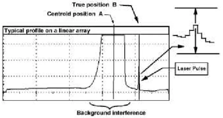
Many devices have been built or considered in the past for measuring the position of a light beam. Among those, one finds continuous response position sensitive detectors (CRPSD) and discrete response position sensitive detectors (DRPSD) [9-20]. The category CRPSD includes lateral effect photodiode and geometrically shaped photo-diodes (wedges or seg-mented). DRPSD on the other hand comprise detectors such as Charge Coupled Devices (CCD) and arrays (1-D or 2-D) of photodiodes equipped with a multiplexer for sequential reading. One cannot achieve high measurement speed like found with continuous response position sensitive detectors and keep the same accuracy as with discrete response position sensi-tive detectors. On Figure 1, we report two basic types of devices that have been proposed in the literature. A CRPSD pro-vides the centroid of the light distribution with a very fast response time (in the order of 10Mhz) [20]. On the other hand, DRPSD are slower because all the photo-detectors have to be read sequentially prior to the measurement of the location of the real peak of the light distribution [21]. People try to cope with the detector that they have chosen. In other words, they pick a detector for a particular application and accept the tradeoffs inherent in their choice of a position sensor. Consider the situation depicted on Figure 2, a CRPSD would provide A as an answer. But a DRPSD can provide B, the desired re-sponse. This situation occurs frequently in real applications. The elimination of all stray light in an optical system requires sophisticated techniques that increase the cost of a system. Also, in some applications, background illumination cannot be completely eliminated even with optical light filters. We propose to use the best of both worlds. Theory predicts that a CRPSD provides very precise measurement of the centroid versus a DRPSD (because of higher spatial resolution). By pre-cision, we mean measurement uncertainty. It depends among other things on the signal to noise ratio, the quantization noise, and the sampling noise. In practice, precision is important but accuracy is even more important. A CRPSD is in fact a good estimator of the central location of a light distribution. Accuracy is understood to be the true value of a quantity. DRPSD are very accurate (because of the knowledge of the distribution) but can be less precise (due to spatial sampling of the light distribution).
Figure 2 A typical situation where stray light blurs the measurement of the real but much narrower peak. A CRPSD would provide A as an answer. But a DRPSD can provide B, the desired response peak.
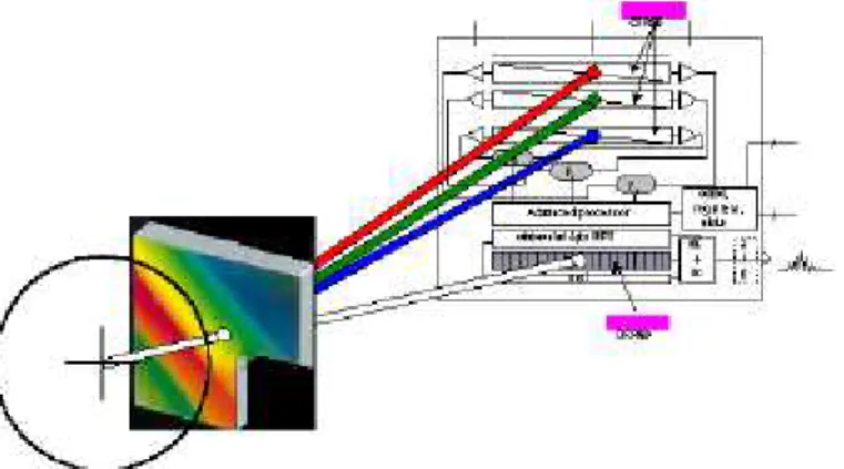
Their slow speed is due to the fact that all the pixels of the array have to be read but they don’t all contribute to the computation of the peak. In fact, what is required for the measurement of the light distribution peak is only a small portion of the discrete detector. Hence the new smart detector. Once the pertinent light distribution is available, one can compute the location of the desired peak very accurately. Figure 3 shows an example of the embodiment of the new smart position sensor for single light spot measurement in the context of 3D and colour measurement. An object is illuminated by a colli-mated RGB laser spot and a portion of the reflected radiation upon entering the system is split into four components by a diffracting optical element. The white zero order component is directed onto the DRPSD, while the RGB 1st order compo-nents are directed onto three CRPSD which are used for colour detection. The CRPSDs are also used to find the centroid of the light distribution impinging on them and to estimate the total light intensity. The centroid is computed on chip or off-chip with the well-known current ratio method i.e. (I1-I2)/(I1+I2) where I1 and I2 are the currents generated by that type of sensor [20]. The centroid value is fed to a control unit that will select a sub-set of contiguous photo-detectors on the
DRPSD. That sub-set is located around the estimate of the centroid supplied by the CRPSD. Then, the best algorithms for peak extraction can be applied to the light distribution of interest, e.g. see [21].
IMPLEMENTATION AND EXPERIMENTAL RESULTS
We present here the architecture and preliminary experimental results of a first prototype chip of a DRPSD with select-able readout window. This is the first block of a more complex chip that will include all the components illustrated in Fig-ure 3. The prototype chip consists of an array of 32 pixels with related readout channels and has been fabricated using a 0.8µm commercial CMOS process [22]. The sensor architecture is typical for linear array optical sensors [23] and is shown in Figure 4. The novelties implemented consist in a variable gain of the readout channels and a selectable readout window of 16 contiguous pixels. Both features are necessary to comply with the requirements of 3D single spot vision systems, i.e. a linear dynamic range of at least 12 bits and a fast readout. Of course, in the prototype, many of the signals which, in the final system are supposed to be generated by the CRPSDs, are now generated by means of external circuitry. As stated above the photosensor array contains 32 pixels with a pitch of 50µm, each pixel having a sensitive area of 48 x 500 µm2. The large dimensions of the pixel are, required, on one side to cope with speckle noise [8] and, on the other side, to facili-tate system alignment. Each pixel is provided with its own readout channel for parallel reading. The channel contains a charge amplifier (CA) and a correlated double sampling circuit (CDS). To span 12 bits of dynamic range, the integrating capacitor of the CA can assume five different values (CAP). In the prototype chip the proper integrating capacitor value is externally selected by means of the switches C0-C4. In the final sensor, however, the proper capacitance value will be automatically set by an on chip circuitry, on the basis of the total light intensity as calculated by the CRPSDs. During nor-mal operation all 32 pixels are first reset at their bias value and then left to integrate the light for a period of 12µs. Within this time the CRPSDs and an external processing unit are supposed to estimate both the spot position and its total intensity and to feed those parameters to the window selection logic, LOGIC_A, and to the gain selection logic, LOGIC_B. After that, 16 contiguous pixels, as addressed by the window selection logic, are read out in 52µs, for a total frame rate of 64µs.
Figure 3 Artistic view of a smart sensor for accurate, precise and rapid light position measurement.
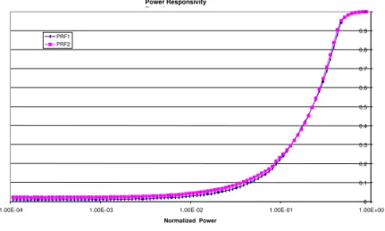
The window selection logic, LOGIC_A, receives the address of the central pixel of the 16 pixel and calculates the ad-dress of the starting and ending pixel. The analog value at the output of the each CA within the adad-dressed window is se-quentially put on the bitline by a decoding logic, DECODER, and read by the video amplifier. LOGIC_A generates also synchronisation and end-of-frame signals which are used from the external processing units. LOGIC_B, instead, is devoted to the generation of logic signals that drive both the CA and the CDS blocks. To add flexibility also the integration time can be changed by means of the external switches T0-T4. The chip has been tested and its functionality has been proven to be in agreement with specifications. In Figures 5 and 6 are illustrated the experimental results relative to spectral responsivity and power responsivity, respectively.
CA CAP CDS CA CAP CDS CA CAP CDS DECODER LOGIC_A BUFFER LOGIC_B SELCAP Φ1-Φ4 FEED RESCAN SEL W0-W4 C0-C4 T0-T4 AUTO START CK RES OUT-VIDEO ENDC SYNC
PIXEL_1 PIXEL_2 PIXEL_32
bitline
Figure 4 Block diagram of the 32 pixel prototype array
Spectral Responsivity Function (SRF)
0 0.05 0.1 0.15 0.2 0.25 0.3 430 480 530 580 630 680 730 780 830 880 930 980 1030 λλ [nm] [A/W]
Figure 5 Spectral responsivity of the photoelements
The spectral responsivity, obtained by measuring the response of the photoelements to a normal impinging beam with varying wavelength is in agreement with data reported in literature [ 23]. Its maximum value of ~0.25 A/W is found around
λ~660nm. The several peaks in the curve are due to multiple reflection of light passing through the oxide layers on top of the photosensitive area. The power responsivity has been measured by illuminating the whole array with a white light
source and measuring the pixel response as the light power is increased. As expected the curve can be divided into three main regions: a far left region dominated by photoelement noise, a central region where the photoelement response is lin-ear with the impinging power and a saturation region. The values of the slope, linlin-earity and dynamic range of the central region have been calculated for three chips and are shown in Table 1.
Power Responsivity Function 0 0.1 0.2 0.3 0.4 0.5 0.6 0.7 0.8 0.9 1
1.00E-04 1.00E-03 1.00E-02 1.00E-01 1.00E+00
Normalized Power
PRF1 PRF2
Figure 6 Normalized power responsivity measured on two different samples.
The capability of the sensor of detecting the spot position has been measured by scanning a focused laser spot over the ar-ray at different speeds. Figure 7 illustrates the response of the sensor for a scanning speed of 12m/s and a spot diameter of 1.8mm. The sensor was operated in free running mode with an effective frame rate of 34µs. Five successive frames are il-lustrated showing the spot entering the array from the right side and exiting from the left side.
Table 1 Relevant electro-optical parameters as calculated by power responsivity measurements Sample # Power Resp. A/W Linearity % Useful Dynamic Range dB 2 0.167 2.9 47 3 0.176 2.9 45 4 0.177 2.8 50 CONCLUSIONS
The results obtained so far have shown that optical sensors have reached a high level of development and reliability that are suited for high accuracy 3D vision systems. The availability of standard fabrication technologies and the acquired know-how in the design techniques, allow the implementation of optical sensors that are application specific: Opto-ASICs. The trend shows that the use of the low cost CMOS technology leads competitive optical sensors. Furthermore post-processing modules, as for example anti reflecting coating film deposition and RGB filter deposition to enhance sensitivity and for colour sensing, are at the final certification stage and will soon be available in standard fabrication technologies.
5.00E-01 1.00E+00 1.50E+00 2.00E+00 2.50E+00 3.00E+00 0 2000 4000 6000 8000 10000 Amplitude [V] frame_1 frame_2 frame_3 frame_4 frame_5 F igure 7 Sensor response to a moving spot laser
REFERENCES
[1] L. Gonzo, M. Gottardi, A. Simoni, and J.-A. Beraldin, “A novel optical bi-cell integrated readout circuitry,” Proceed-ings of the 1999 IEEE International Symposium on Circuit and Systems, Orlando, FL. May 30-June 2, 1999.
[2] J.-A. Beraldin, F. Blais, M. Rioux, L. Cournoyer, D. Laurin, and S.G. MacLean, “Eye-safe digital 3D sensing for space applications,” Opt. Eng. 39(1): 196-211; January 2000. NRC 43585.
[3] Hébert, P. and Rioux, M., Toward a hand-held laser range scanner: integrating observation-based motion compensa-tion, IS&T/SPIE’s 10th Intern. Symp. Electronic Imaging, 24-30 Jan., 1998.
[4] P.J. Besl, “Range Imaging Sensors,” Machine Vision and Applications (1), 127-152, 1988.
[5] J.-A. Beraldin, F. Blais, L. Cournoyer, M. Rioux, S.H. El-Hakim, R. Rodella, F. Bernier, N. Harrison, “3D Digital Im-aging and Modeling on Remote Sites,” Proceedings Second Intern. Conf. on 3D digital imIm-aging and modelling, Ot-tawa, Canada, pp. 34-43, 1999.
[6] M. Rioux, “Laser Range Finder based on Synchronized Scanners,”' Appl. Opt., 23, 3837-3844, 1984.
[7] F. Blais, M. Lecavalier, J. Domey, P. Boulanger, and J. Courteau, “Application of the BIRIS Range Sensor for Wood Volume Measurement,” NRC-ERB-1038, October, 1992.
[8] R. Baribeau, and M. Rioux, “Influence of Speckle on Laser Range Finders,” Appl. Opt., 30, 2873—2878, 1991. [9] R.F. Lyon, and M. P. Haeberli, “Designing an testing the optical mouse”, VLSI DESIGN Jan-Ffeb, pp.20-30, 1982. [10] A. Mäkynen and J. Kostamovaara, “Linear and sensitive CMOS position-sensitive photodetector,” Electronics letters,
Vol. 34 (12), pp.1255-1256, June 1998.
[11] P. Aubert, H.J. Oguey and R. Vuilleunier, “Monolithic optical position encoder with on-chip photodiodes,” IEEE Journal of solid-state circuits, Vol. 23 No.2, April, pp. 465-473, 1988.
[12] T. Matoba, M. Kawai and Y. Ono, “Photosensor array for optical encoder,” Electronics and communications in Japan, Part 2 Vol. 75, No.1, pp.56-63, 1992.
[13] C. During, “Real time optical measurement of position,” Mechatronics, vol4 no.2 pp.125-138, 1994.
[14] K. Engelhardt, and P. Seitz, “Absolute high-resolution optical position encoder,” Applied Optics, 1 Jan. 1996, Vol.35, No.1 pp.201-208
[15] D. J. Bernays, “The use of Ronchi rulings for high precision two-dimensional galvo deflection systems,” SPIE Vol.498, Laser Scanning and Recording, pp.175-182, 1984.
[16] X. Arreguit, F.A. van Schaik, F.V. Bauduin, M. Bidiville, and E. Raeber, “A CMOS motion detector system for pointing devices,” IEEE Journal of solid-state circuits, Vol. 31 No.12, Dec, pp.1916-1921, 1996.
[17] A. Simoni, A. Sartori, M. Gottardi, and A. Zorat “An intelligent linear image sensor, ” in Proc 19th ESSCIRC, Seville Spain, p.246-249, 1993.
[18] S. K. Mendis, S.E. Keneny, R.C. Gee, B. Pain, C.O. Staller, Q. Kim and E.R. Fossum “CMOS Active Pixel Image Sensor for Highly Integrated Imaging Systems,” IEEE J. Solid-State Circuits, SC33, pp.824-849, 1998.
[19] A. Simoni, G. Torelli, F. Maloberti, A. Sartori, S. Plevridis, “A Single Chip Optical Sensor with Analog Memory for Motion Detection,” IEEE J. Solid-State Circuits, 30, pp.800-806, 1995.
[20] J.-A. Beraldin, “Design of Bessel-type Pre-Amplifiers for Lateral Effect Photodiodes,” Int. J. Electron., 67, 591-615, 1989.
[21] F. Blais, M. Rioux, J.-A. Beraldin, “Practical considerations for a design of a high precision 3-d laser scanner system,” Optomechanical and Electro-Optical Design of Industrial Systems, SPIE Vol. 959, p. 225-246, 28-29 June, 1988. [22] AMS - Austria, http://www.amsint.com
[23] P. Lee, A. Simoni, A. Sartori, and G. Torelli, “A Photosensor Array for Spectrophotometry, Sensors and Actuators,” A Physical, Vol 46-47, p. 449-452, 1995.