Block Copolymer Photonic Crystals:
Towards Self-Assembled Active Optical Elements
by
Jongseung Yoon
B.Sc. Fiber and Polymer Science, Summa Cum Laude Seoul National University, February 1996
Submitted to the Department of Materials Science and Engineering In Partial Fulfillment of the Requirements for the Degree of
DOCTOR OF PHILOSOPHY
IN
POLYMERS at theMASSACHUSETTS INSTITUTE OF TECHNOLOGY June 2006
O
2006 Massachusetts Institute of Technology. All rights reserved.n
IARCH
WE8
0
C / r-/...
...
Signature of Author:
(/.
Department of Materials Science and Engineering May 26,2006
Certified by:
...
rr.Nw.-.. .-.
....
..
-.7-.
...
/
Edwin L. ThomasMorris Cohen Professor of Materials Science and Engineering Thesis Supervisor 4
...
..
...
.
Accepted by:...
/
.Y . w . r . r . . U. .r.. .L.. .=. Samuel M. Allen POSCO Professor of Physical Metallurgy Chairman, Department Committee on Graduate StudentsBlock Copolymer Photonic Crystals:
Towards Self-Assembled Active Optical Elements
byJongseung Yoon
Submitted to the Department of Materials Science and Engineering on May 26,2006 in Partial Fulfillment of the Requirements for the Degree of
Doctor of Philosophy in Materials Science and Engineering
Block copolymers have proven to be a unique materials platform for easily fabricated large-area photonic ~crystals. While the basic concept of block copolymer based photonic band gap materials has been well ~demonstrated, little work has been achieved yet in terms of realizing optically active devices using these materials. :[n this thesis, the utilization of block copolymer photonic crystals for creating self-assembled active optical lelements has been experimentally explored with a special emphasis on optically driven lasing and stimulus :responsive tunable reflectors. In pursuing these primary objectives, control of thin film microdomain orientation ,and novel three-dimensional (3D) optical characterization of block copolymer photonic crystals have been also ,acheved, both of which can greatly help optimize the properties of block copolymer photonic crystals.
First, a laser cavity using block copolymer based one-dimensional (ID) photonic crystals has been 'demonstrated. Optically pumped surface-emitting lasing has been obtained using a dye-doped polymers as the ,organic gain medium and the self-assembled block copolymer as the spectral-band selective distributed Bragg reflector feedback element. We also developed a novel organiclinorganic hybrid photonic crystal containing a dye- 'doped defect layer for defect-mode photonic bandgap lasing. Low threshold lasing has been demonstrated at a single defect-mode wavelength of the 1D photonic bandgap structure resulting from the inhibited density of states ,of photons within the stop band and the enhanced rates of spontaneous emission at the localized resonant defect mode.
Second, stimulus responsive tunable self-assembled reflectors based on 1D block copolymer photonic crystals have been studied. Three external stimuli such as solvent, temperature, and compressive mechanical strain have been employed to modulate microstructural and material properties of block copolymer photonic crystals, resulting in effective tuning of the spectral characteristics of block copolymer photonic structures.
Finally, control of the microdomain orientation of 1D and 2D block copolymer photonic crystals has been achieved over a large area via directional solidification of solvent. Moreover, an intriguing ordering behavior of these ultrahigh molecular weight block copolymers has been revealed, which is dramatically different from that of typical molecular weight block copolymers. These highly oriented thin film microdomain patterns have been explored via 3D optical imaging using laser scanning confocal microscopy.
Thesis Supervisor: Edwin L. Thomas
TABLE OF CONTENTS
List of Figures
...
6List of Tables
...
15Acknowledgements
...
16Foreword
...
18Motivation and Objective
...
18...
Thesis Overview 19
Chapter 1
.
Introduction to Block Copolymer based Photonic Bandgap Materials...
1.1. Photonic Crystals...
1.2. ID, 2D. and 3D Block Copolymer Photonic Crystals...
1.3. Nanocomposite Block Copolymer Photonic Materials...
...
1.4. Switchable Block Copolymer Photonics
...
...
...
...
1.5. Challenges. Advantages. and Applications1.6. References
...
Chapter 2.
Materials and Experimental Methods...
...
2.1. High Molecular Weight Block Copolymers
...
...
2.1.1. Purification of glassware, syringes. needles...
2.1.2. Purification of solvents2.1.3. Purification of monomers
...
2.1.4. Polymerization and molecular characterization...
...
2.2. Microstructural Characterization2.2.1. Solution casting
...
...
2.2.2. Cryomicrotomy and transmission electron microscopy (TEM)....
2.2.3. Laser scanning confocal microscopy (LSCM)...
2.2.4. Ultrasmall angle X-ray scattering (USAXS)...
2.3. Optical Characterization...
...
2.3.1. Reflectivity measurement
...
2.3.2. Absorption and emission measurements...
2.3.3. Lasing measurements...
....
...
...
2.4. References...
...
Chapter 3. Defect-Mode Mirror-less Lasing in a Dye-doped Organicnnorganic
...
59 Hybrid 1D Photonic Crystal3.1 Introduction e . . e . . . e . . ~ . . . e ~ ~ ~ ~ o e m o e e e ~ ~ e e e m e e e e e e e e e 60
3.2 Results and Discussion ~ e ~ ~ e ~ ~ e ~ e ~ ~ ~ ~ e ~ ~ ~ ~ ~ ~6 1 e ~ ~ e ~ e ~ ~ ~ ~ ~ ~ ~ ~ e ~ ~ e ~ e e e e e e e e e e 3.3 Conclusion ~ ~ ~ ~ ~ ~ e ~ ~ e ~ e ~ ~ ~ ~ ~ ~ ~ ~ e ~ ~ ~ ~7 1 ~ e ~ e e e e ~ e e e e e e e e e e e e e e e
3.4 References . . . e . . . . . e . . . ~ . . . . . . . . e ~ ~ m e * ~ e ~ ~ ~ ~ o e ~ e m ~ e e e e e e e e e e e e 73 Chapter 4. Optically Pumped Surface-Emitting Lasing using Self-As~embled...~.~.... 76 Distributed Bragg Reflectors from 1D Block Copolymer Photonic Crystal
4.1 Introduction . . e . . . e . . ~ . . . e m o e ~ o e ~ ~ ~ ~ ~ e ~ ~ e e e e e e e e e e e e e e e e 77
4.2 Results and Discussion ~ ~ ~ ~ ~ ~ ~ ~ ~ ~ ~ e ~ ~ ~ ~ ~ 78 e ~ ~ e ~ ~ e ~ ~ ~ ~ ~ ~ ~ ~ ~ ~ ~ ~ m e ~ ~ e e e e ~ e e ~ e e e e e
4.3 Conclusion ~ ~ ~ ~ ~ ~ ~ ~ ~ ~ ~ ~ ~ ~ 90 ~ ~ e ~ ~ e ~ ~ ~ ~ ~ e ~ ~ ~ ~ e e e e e e e e e e e
4.4 References . . e. . e .. e . . e. . . . .. . . . .. . . e ~o e ~ o e ~~ e ~ ao ~ ~ e ee e ee e ee e ee e e 91 Chapter 5. Chemically, Thermally, Mechanically Responsive Tunable
...
94 Self-Assembled Reflectors based on Block Copolymer Photonic Crystals5.1 Introduction
...e...e...
955.2 Results and Discussion ~ ~ e ~ e ~ ~ ~ e ~ ~ ~ ~ ~ ~ ~ ~ ~ e 96 e ~ ~ ~ ~ ~ e ~ ~ ~ ~ ~ e ~ ~ ~ ~ ~ ~ ~ e e e e e e e e e e e e
5.3 Conclusion ~ e ~ ~ e ~ ~ e ~ ~ ~ ~ ~ ~ ~ ~ ~ ~ ~ ~ ~ 123 e ~ ~ e ~ ~ e ~ ~ e e ~ e e e e e e e e e e e e e
5.4 References ... 126 Chapter 6. Highly Oriented Thin Film Microdomain Patterns of Ultrahigh
...
129 Molecular Weight Photonic Block Copolymers via Directional Solidificationof a Solvent
6.1 Introduction . . e . . . e e . . . . . . . . e . e . . e ~ ~ ~ ~ a e ~ ~ e ~ o e ~ ~ ~ ~ ~ e e e130 e e e e e
6.2 Results a d Discussion ~ ~ ~ ~ ~ e ~ ~ e ~ ~ e 13 1 ~ ~ ~ ~ ~ ~ ~ ~ ~ ~ ~ ~ ~ e ~ ~ ~ ~ e e e e e e e ~ e
6.3 Conclusion. ~ ~ ~ e ~ ~ e ~ ~ ~ ~ ~ e ~ e e ~ ~ ~ ~ ~ ~ ~ 143 e ~ ~ ~ ~ ~ e e e e e e e e e e e e e e e e e 6.4 References
...
.e...8...8...e..e....e....e.
145Chapter 7. Summary and Future Work
...
...
149 7.1. Research Summary ~ . e ~ ~ . . m e . . e . . . . . . . ~ . . . . . e ~ o ~ ~ ~ ~ ~ e e e e ~ e e e e 1 e50 m e7.2. Future Work ~ ~ ~ e ~ ~ ~ ~ ~ ~ ~ e ~ m e ~ ~ ~ ~ ~ e ~ ~ ~ ~ 152 ~ ~ ~ e ~ m ~ ~ ~ e ~ ~ e ~ ~ e e e e m e e e e e e e e e m e 7.3. References . e ~ . . . . . m . . . . . . ~ . . . . . . . . . m e ~ o e ~ ~ e ~ ~ ~ ~ ~ ~ ~ e e e e e e e e e157 e
Appendix
.
Polyolefin based Photonic Bandgap Materials
....m....m...
A.
1 Introduction...
A.2 Experimental...
A.2.1.1. Synthesis...
. .
A.2.1.2. Charactenzatlon...m..m..m..m...
A.3 Results and Discussion...
A.4 Conclusion
...
A.5 References...
LIST OF FIGURES
Figure 1.1: A schematic diagram of ID, 2D, 3D periodic photonic crystals composed of high (blue) and low (green) refractive index domains. This diagram was adopted from [5].
Figure 1.2: A schematic diagram showing various bulk morphologies of linear diblock copolymer, poly(A-b-B), as a function of volume fraction of A block (The double diamond bicontinuous network structure does not occur for simple diblocks). This diagram was
...
adopted from Dr. Banita Dair. 27
Figure 1.3: ID, 2D, 3D photonic crystals from (a) lamellar (from [26]) (b) cylindrical (from [32]) and (c) double gyroid (from [36]) morphologies of PS-b-PI block copolymers, respectively. Figure 1.3(a) is a TEM image of an Os04 stained PS-b-PI diblock, Figure 1.3(b) is an AFM image of cylindrical PS-b-PI diblock, Figure 1.3 (c) is a SEM image of ozone-etched double gyroid PS-b-PI diblock.
...
28 Figure 1.4: A band diagram (dimensionless frequency vs. dimensionless wavevector) using the refractive indices of polystyrene (rips = 1.59) and polyisoprene (npI = 1.5 1) and the layer thicknesses of a PS-b-PI block copolymer (dps = dpI = 100 nm). The transverse-electric (TE) polarization modes are on the right side, and the left side is for the transverse- magnetic (TM) polarized light. The numerical code was written by Dr. Martin Maldovan at MIT. (c: speed of light in a vacuum, a: lamellar domain periodicity = dps+dpl)...
30 Figure 1.5: Reflectivity plot constructed by the transfer matrix method for a 20-period stack of alternating PS (n = 1.59) and PI (n = 1.51) layers (glass substrate-(PS layer-PI layer120-air), for TM (left) and TE polarization (right), respectively. Each layer is assumed to be 100 nm thick. The color represents the strength of the reflectivity at a particular.
polarization, frequency, and angle of incidence of incident light....
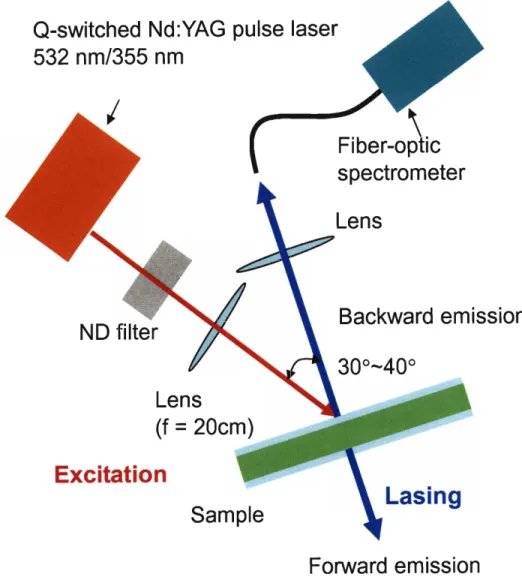
3 1 Figure 2.1: A schematic of the experimental setup for measuring emission and lasing spectra ... 57Figure 3.1 : Bright-field TEM micrograph of surface-protected titania (Ti02) nanoparticles on carbon film, in which well-dispersed and monodisperse nanoparticles having an average diameter of about 4 nm are evident.
...
62 Figure 3.2: Powder XRD spectrum of surface-protected titania (Ti02) nanoparticles, in...
which the reflection peaks are well matched with those of anatase phase titania. 63Figure 3.3: Linear absorption and photoluminescence spectra of DCM (0.5 wt %, 400 nm excitation) in PMMA. The molecular structure of DCM is shown in the inset. The FWHM of the PL spectrurn is about 75 nm and the peak of the spontaneous emission occurs at 582 nm.
...
63 Figure 3.4: Schematic of dye-doped defect-mode 1D photonic crystal, glass-(PMMA-15 15
.
...
Ti02) -(DCM/PMMA)-(Ti02-PMMA) -air. 65
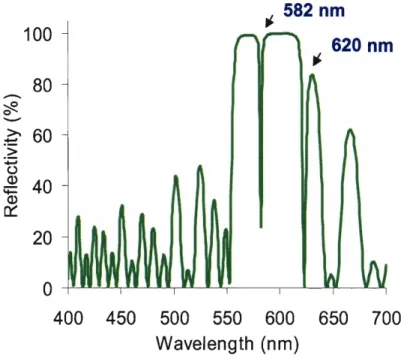
Figure 3.5: TMM calculated reflectivity spectrum of the defect-mode 1D photonic crystal, g l a s s - ( ~ ~ ~ ~ - ~ i 0 2 ) 1 5 - ( ~ ~ ~ / P ~ ~ ~ ) - ( ~ i ~ 2 - ~ ~ ~ ~ ) 1 5 - a i r , at normal incidence. Arrows indicate the localized defect-modes created by the PMMA defect layer
...
66 Figure 3.6; Calculated density of states of photons, p(o)= dkldo, of the defect-mode 1D
photonic crystal, g l a s s - ( ~ ~ ~ ~ - ~ i 0 2 ) 1 5 - ( ~ ~ ~ / P ~ ~ ~ ) - ( ~ i 0 2 - ~ ~ ~ ~ ) 1 5 - a i r , in which the
..
y-axis shows the normalized p(o) with respect to the value in vacuum (p(w),,,= llc). 66
Figure 3.7: Measured reflectivity spectrum of the fabricated defect-mode 1D photonic crystal at near normal incidence using a reflection-mode optical microscope connected to a fiber-optic spectrometer, in which the spectrum represents a convolution of multiple reflectivity spectra over the incidence angles of 0" to ~ 1 7 . 5 ~ due to the numerical aperture of the objective lens ( l o x , N.A. = 0.3). Experimental features indicative of the two defect
...
...
modes are shown..
.
.
.
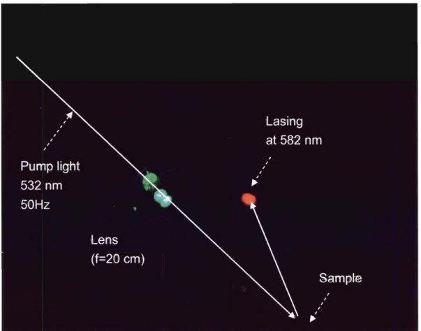
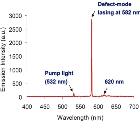
67Figure 3.8: Photograph of the 582 nm lasing from the defect-mode 1-D photonic crystal. A highly directional lasing in the backward direction was observed on a white background.
Figure 3.9: The lasing spectrum obtained at a pump power of 1 mW, above the lasing threshold. The two small peaks beside the lasing line at 582 nm correspond to the excitation light (532 nm) and to the low frequency defect mode (at 620 nm, below its lasing threshold for this pump power).
...
70 Figure 3.10: Emission intensity and line-width (the full width at half maximum, FWHM) at the lasing wavelength (582 nm) as a function of pump power. The behavior of the intensity and the FWHM clearly demonstrate a threshold for lasing around 0.6 mW pump power (12 pJ pulse energy)....
70 Figure 4.1: Bright-field TEM micrograph of cryomicrotomed PS-b-PI block copolymer showing a 1D periodic lamellar morphology, in which the dark regions correspond to PI domains preferentially stained with Os04 and the bright regions correspond to PS domains. The domain periodicity is approximately 140 nm (PS : 76 nm, PI: 64 nrn)....
79 Figure 4.2: Experimental reflectivity spectrum of the fabricated block copolymer based distributed Bragg reflector at near normal incidence using a reflection-mode optical microscope connected to a fiber-optic spectrometer. The inset shows a calculated reflectivity spectrum using the transfer matrix method at a normal incidence for a finite 1D periodic structure, assuming 300 layers of PS (76 nm, n = 1.59) and PI domains (64 nm, nFigure 4.3: Photoluminescence (PL) spectrum from a solid film of Bis-MSB (0.1 wt %, 355 nm excitation) in PMMA. The FWHM of the PL spectrum is about 75 nm. The inset shows the absorption spectrum from the same sample, where the absorption maximum is located at around 350 nm... 82
Figure 4.4: Schematic of the block copolymer based laser cavity, comprised of a gain medium, Bis-MSB and PMMA, enclosed between two block copolymer based distributed Bragg reflectors. The thicknesses of PS and PI domains are estimated values at 10 wt % solvent concentration based on the peak position and FWHM of the reflectivity spectrum.
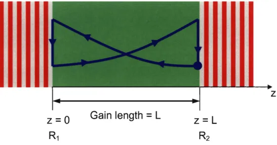
Figure 4.5: A model laser cavity composed of a gain medium (length L) and two dielectric mirrors having reflectivity values of R1 (z = 0) and Rz (z = L). The blue arrow represents
. .
.
.the power of the oscillating radiation.
...
84 Figure 4.6: Photograph of the 410 nm lasing fiom the block copolymer based laser structure. A highly directional lasing output in the backward direction was observed on a white background....
86 Figure 4.7: The emission spectra obtained at various pump powers. The FWHM of the lasing peak is 1 nm. Inset shows the emission intensity at the lasing wavelength (410 nm) as a function of pump power, which clearly shows a threshold for lasing at around 4 mW pump power (0.2 mJ pulse energy)....
88 Figure 4.8: Lasing spectrum fiom a solid film of Bis-MSB (0.1 wt %) in PMMA sandwiched between an aluminum-coated mirror and a glass slide pumped by 355 nm pulse laser, where the lasing peak occurs at 425 nm and the FWHM is 4 nm. The inset shows a schematic of the sample...
...
...
...
89 Figure 5.1: A schematic of a model 1D photonic crystal, air-(high index layer-low index layer)N-glass substrate, with incident electromagnetic wave of a transverse-electric (TE) polarization (the electric field vector (E) is perpendicular to the plane of incidence or parallel to the z-axis (z))....
97 Figure 5.2: Reflectivity spectra of model 1D photonic crystals at normal incidence as a function of the domain periodicity (L = dH+ dL, dH
= dL), assuming constant refractive indices (nH = 1.59, n~ = 1.51) and fixed total number of layers (2N = 50). The peak reflectivity wavelength at each domain periodicity is shown in the inset....
....
98 Figure 5.3: Reflectivity spectra at normal incidence of a model 1D photonic crystal (Figure 5.1) as a function of the refractive index contrast (nH/nL), assuming constant domain...
thicknesses (dH = dL = 100 nrn) and a fixed total number of layers (2N =20). 100incidence as a fimction of refractive index contrast (nH/nL) and a total number of layers (2N) from Equation 5.1. (dH = hd4nH, dL = ho/4nL, ki: incident wave vector, k,: reflected wave vector, kt: transmitted wave vector).
...
100 Figure 5.5: Schematic of 1D photonic crystals having different domain orientations with respect to a certain direction of incident light (ki), (a) 8 = 0°, (b) 8 > 0"...
101 Figure 5.6: Reflectivity map computed by TMM for a 15-period (2N = 30) stack of alternating high and low index layers for (a) low refractive index contrast (nH/nL =1.5911.5 1) and (b) high refractive index contrast (nH/nL = 2.2711.5 1) for TE (right) and TM (left) polarizations, assuming quarter-wave layer thicknesses of 500 nm and total 30 layers. The color represents the strength of the reflectivity at a particular frequency, a polarization, and an angle of incidence. The omnidirectional reflectivity band is shown for the high
...
refractive index contrast 1 D photonic crystal. 102
Figure 5.7: Bright field TEM micrograph of crymicrotomed PS-b-PI block copolymer, in which PI domains are preferentially stained with Os04. The domain periodicity fiom the TEM micrograph is approximately 200 nm (PS: 1 10 nrn, PI: 90 nm).
...
104 Figure 5.8: A series of pictures taken from confined block copolymer gel at different solvent evaporation times (e.g. 2:40 means 2 h 40 min). These pictures were taken by Felice Frankel at MIT....
105 Figure 5.9: Reflectivity spectra taken in the early stage of solvent evaporation at various radial positions from the center to the edge with normal incident light using a microscope spectrometer. Note the continuous change in the peak wavelength with radial distance fiom the sample center. The sample in the photograph appears to the eye as having a large single color near the center, but the measured spectra show a significant variation of the actual. .
color with radial position.
...
106 Figure 5.10: Effective refractive indices of PS (thick line) and PI (thin line) microdomains as a function of solvent concentration at various solvent refractive indices, (a) n, = 1.61 > n~ > n ~ , (b) n~ > n, = 1.55 > n ~ , (c) n~ > n~ > n, = 1.49. Case (c) is relevant to the...
Figure 5.11: Average effective refractive indices (navg = (hff, H
+
&& =)/2) as a function of solvent concentration at various solvent refractive indices, (a) n, = 1.6 1 > n~ > n ~ , (b) n~ > n, = 1.55 > n ~ , (c) n~ > n~ > n, = 1.49. Case (c) is relevant to the experiments on PS-b-PI with cumene (n = 1.49)...
11 1 Figure 5.12: Measured reflectivity spectra of the block copolymer lamellar photonic gel at various temperatures between 30 "C and 140 "C....
1 13 Figure 5.13: Peak reflectivity wavelengths obtained from TMM calculations with temperature-dependent refractive indices (red data points), with temperature-dependent domain thicknesses (blue data points), and with both temperature-dependent refractive indices and domain thicknesses at various temperatures. The observed peak reflectivity wavelengths (black data points) are also sho wn... 120Figure 5.14: Measured peak reflectivity wavelength (blue data points) versus sample thickness of mechanochromic block copolymer gel. The orange line is obtained from the TMM calculation. Inset shows photographs taken from the sample at different sample thicknesses.
...
122 Figure 6.1: Reflection mode LSCM image (xy-scan) of PS-b-PI block copolymers showing highly-oriented lamellar microdomains in a thin film obtained from directional solidification process with benzoic acid (BA). Inter-material dividing surfaces (IMDSs) are principally aligned perpendicular to the fast growing direction of benzoic acid (the b-axis of BA crystal). The inset is a high magnification image of the edge-on lamellae, for which the lamellar periodicity (dLAM-
2 10 nm) is shown....
133 Figure 6.2: Reflection mode LSCM image (xy-scan) of PS-b-PI block copolymers showing highly-oriented cylindrical microdomains in a thin film obtained from directional solidification process with benzoic acid (BA). Inter-material dividing surfaces (IMDSs) are principally aligned perpendicular to the fast growing direction of benzoic acid (the b-axis of BA crystal) The inset is a high magnification image of the in-plane cylinders, for which the inter-cylinder spacing (dcuL-
260 nm) is shown....
134Figure 6.3: A low magnification LSCM image (xy-scan) of SICYL showing the relative orientation of cylindrical microdomains with respect to the fast-growth direction of BA crystal.
...
135 Figure 6.4: 3D reconstruction of reflection mode LSCM image of a highly-ordered lamellar PS-b-PI block copolymer in a thin film obtained from the DS process. 3D imaging revealed that larnellae were tilted by about 60" to the fast-growth direction of BA. Corresponding schematic with the direction of BA crystallization is also shown....
136 Figure 6.5: 3D reconstruction of reflection mode LSCM image of a highly-ordered cylindrical PS-b-PI block copolymer in a thin film obtained from the DS process. 3D imaging revealed cylindrical microdomains were hexagonally packed in the xz-plane. Corresponding schematic with the direction of BA crystallization is also shown....
137 Figure 6.6: Reflection-mode LSCM images (xy-scan) of PS-b-PI block copolymer (SICYL) taken every 220 nm along the z-axis on the same sample position. In each figure, three circled regions show the alternating registration of PS cylindrical domains (bright region) in PI matrix (dark region) along the z axis....
138 Figure 6.7: Schematic diagrams showing the hypothetical concentration profiles of block copolymer (@BCP) along bBA, the fast-growth direction of benzoic acid (BA) crystal during the DS process for (a) high and (b) low molecular weight block copolymer samples. The dotted lines represent BA crystallization front (a) and block copolymer microphase separation front(P).
The insets show respective schematics of corresponding microdomain...
orientations with respect to bBA induced during the DS process. 141Figure 7.1: Emission spectra of the self-assembled distributed feedback (DFB) laser structure enabled with PS-b-PI (320W270k) block copolymer and Bis-MSB. The inset shows the pump power dependence of emission intensity of the block copolymer based DFB structure.
...
153 Figure A.1: Refractive index as a fbnction of wavelength for polyolefin random copolymers measured by a spectroscopic ellipsometry, (a) poly(E-co-N) (entry 1 in Table I),(b) poly(MCP-co-VTM) (entry 3), (c) poly(E-co-P) (entry 2).
...
168 Figure A.2: Bright field TEM micrograph of cryomicrotomed section of the poly[(MCP- co-VTM)-b-(E-co-N)] block copolymer showing a lamellar morphology (domain periodicity-
170 nm). The dark regions (IMCP-co-VTM = 68 nm) correspond to poly(MCP-co- VTM) microdomains preferentially stained with osmium tetroxide (Os04) and the bright...
regions (IE-co-N = 102 nm) are poly(E-co-N) microdomains. 169Figure A.3: Measured reflectivity spectrum of poly[(MCP-co-VTM)-b-(E-co-N)] lamellar film by a CARY spectrophotometer equipped with a difisive reflectivity accessory. The peak reflectivity wavelength is around 470 nm
...
172 Figure A.4: Calculated reflectivity map of a multilayer stack having the same layer thickness and refractive index as poly[(MCP-co-VTM)-b-(E-co-N)] as a function of the incidence angle (x-axis), the polarization (x-axis), and the wavelength (y-axis) of the incident light, assuming the thickness of high (E-co-N)llow (MCP-co-VTM) index layer is 102 d 6 8 m , the refractive index of highllow index layer is 1.5211 SO, and a total number of 100 layers. The inset shows the reflectivity spectrum at normal incidence (incidence angle = 0') as a function of wavelength, in which the peak reflectivity wavelength is 5 15 nm...
173 Figure A.5: Bright field TEM micrograph of cryomicrotomed section of the poly[(E-co-P)- b-(E-co-N)], in which the domain periodicity is 91 nm (IE-co-N = 56 nm, lE-co-P = 35 nm). The dark regions correspond to poly(E-co-N) microdomains preferentially stained with ruthenium tetroxide (Ru04) and the bright regions correspond to poly(E-co-P) microdomains. Small particle-like entities in the micrographs come from ruthenium. .
tetroxide (staining agent) aggregations
...
175 Figure A.6: Bright field TEM micrograph of cryomicrotomed section of the poly[(E-co-P)- b-(E-co-N)] ternary blend containing 20 wt % (10110) homopolyrners. The domain periodicity is 127 nm (lE-co-N = 79 nm, lE-co-p= 48 nm)...
...
176b-(E-co-N)] ternary blend containing 40 wt % (10110) homopolymers. The domain
. . . .
periodicity is 152 nm (ZE-co-N = 88 nm, ZE-co-P= 64 nrn)
...
177 Figure A.8: Smeared USAXS 1D line source data obtained from the polyolefin block copolymer films of (a) the poly[(E-co-P)-b-(E-co-N)] and ternary blends of the diblock containing (b) 20 wt % and (c) 40 wt % homopolyrners. The (001) peaks for all three samples correspond well to the lamellar periods measured from TEM micrographs....
178 Figure A.9: Measured reflectivity spectra of (a) the poly[(E-co-P)-b-(E-co-N)] and ternary blends of the diblock containing (b) 20 wt % and (c) 40 wt % homopolymers by a CARY spectrophotometer equipped with a diffusive reflectivity accessory. The peak reflectivity wavelengths are (a) 268 nm (host diblock), (b) 335 nm (20 wt % blend), and (c) 448 nm (40 wt % blend), respectively...
179 Figure A.10: Calculated reflectivity maps (for TE polarization of incident light) of multilayer stacks having the same layer thickness and refractive index as (a) poly[(E-co- P)-b-(E-co-N)], (b) 20 wt%, and (c) 40 wt% ternary blend as a function of the incidence angle (x-axis) and the wavelength (y-axis) of incident light, assuming that the thickness of high (E-co-N)llow (E-co-P) index layers are (a) 56 d 3 5 nm, (b) 79 nm148 nm, (c) 88 nrn164 nm as obtained from TEM, the refractive index of higWlow index layer is 1.5211.47 as obtained from ellipsometry, and a total number of 100 layers....
180LIST OF TABLES
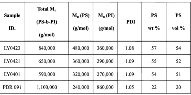
Table 2.1: Molecular characteristics of the four photonic PS-b-PI block copolymers
.
.
used in this thesis.
...
...
5 1 Table 5.1: Calculated normal incidence peak reflectivity wavelengths of a PS-b-PI photonic gel in a range of domain thicknesses with 10 wt % solvent concentration, assuming refractive indices of high and low index layers as 1.580 and 1.508, a fixed ratio of PS and PI domain thicknesses (dpS/dpI = 1.1/0.9), and total 400 layers....
114 Table 5.2: Effective refractive indices and effective domain thicknesses of PS and PI domains at various solvent concentrations determined from TMM calculations, which give a peak wavelength of the corresponding reflectivity spectrum at 5 10 nm....
1 1 5 Table 5.3: Effective refractive indices of PS and PI domains and peak reflectivity wavelengths at various temperatures obtained from TMM calculations, in which the domain spacings of the respective domains are held constant as the estimated values atTable 5.4: Effective domain spacings of PS and PI domains and peak reflectivity wavelengths at various temperatures obtained from TMM calculations, in which the refractive indices of respective domains are held constant as the estimated values at 30 OC.
...
118 Table 5.5: Effective refractive indices, effective domain thicknesses of PS and PI domains, and peak reflectivity wavelengths at various temperatures obtained from TMM calculations...
11 9 Table A.1. Materials data for polyolefin copolymers....
166ACKNOWLEDGEMENTS
Foremost, I am deeply indebted to Prof. Edwin L. Thomas, my Ph.D. advisor for his continuous support, encouragement, and insightful guidance. Ned has been my role model of a great scientist, advisor, and educator. All of my academic achievements at MIT would not have been possible without his sincere dedication to his students and his willingness to share his knowledge, motivation, and ideas.
I am also very grateful to my thesis committee members, Prof. Samuel Allen and Prof. Michael Rubner for their valuable comments and suggestions on my thesis.
I would also like to express my gratitude to my academic advisors at Seoul National University, Prof. Jae-Ryun Youn, and Prof. Won-Ho Jo for their support in my pursuing Ph. D. at MIT.
I have been fortunate over the past years to have many precious collaborators. I am particularly grateful to Dr. Wonrnok Lee for his unselfish mentoring and help in many aspects of my thesis work. It is particularly memorable to me when we made our first breakthrough in the synthesis of ultrahigh molecular weight block copolymers after overcoming many obstacles. I am very grateful to Dr. Robert Mathers and Prof. Geoffrey Coates of Cornell University for their contribution to develop polyolefin based photonic bandgap materials. I would also like to express my gratitude to Dr. Peter DeRege and Dr. Apostolos Avgeropoulos for their useful advice on polymer synthesis. I would like to thank Dr. Jean-Michel Caruge, Dr. Steven Kooi, Dr. Jeff Baur, and Dr. Seong-Ho Cho of MIT for their help on optical measurements. I extend my thanks also to Prof. Rajeev Ram and Prof. Erich Ippen of MIT for their valuable comments on my research.
I am very thankful to Dr. Jinsang Kim and Dr. Cheolmin Park for their mentoring and guidance in my early years at MIT.
I would like to appreciate all members of Thomas group at MIT for their support and friendship, which made my life at MIT enjoyable. In particular, I would like to
acknowledge Augustine Urbas, Michael Bockstaller, Jiwoong Park, Chinedum Osuji, Chaitanya Ullal, Panitam Wanakamol, Ion Bita, Hyunjung Lee, Jihyun Jang, Joe Walish, Rafal Mickiewicz, Nick Tsui, Taeyi Choi, Melinda Cromie, Rachel Pytel, Taras Gorishnyy, and Martin Maldovan.
I also have so many wonderful Korean friends. I thank all Korean friends at MIT for their support and friendship. I extend my thanks to my lifetime friends including Sungjun Im, Woojin Chang, Wanhee Kim, and Youngjo Song.
I am grateful beyond words to my parents, Drs. Hyungwon Yoon and Kyungran Jeon for their unconditional love and sacrifice. I thank my sisters, Sumi and Suyoung, and my brother-in-law, Sangkwon Lee for their continued support. I would also like to express my deep gratitude to my uncle, Seokwon Yoon, and aunts for their endless support and encouragement. Among all I am eternally gratefbl to my grandmother for always believing in me, encouraging me, and teaching me so many invaluable lessons in life.
Foreword
Motivation and Objective
Self-assembled block copolymer systems with an appropriate molecular weight to produce a domain size comparable to the wavelength of light have attained increasing attention as alternative building blocks to fabricate photonic crystals in the visible and near-IR frequencies. ID, 2D, and 3D photonic crystals have been successfully demonstrated with various microdomain structures created through microphase separation of block copolymers. The size and shape of periodic microstructures of block copolymers can be readily tuned by controlling molecular parameters such as molecular weight, relative composition, chain architecture, and persistence length, or by blending with homopolymer or plasticizer. The versatility of block copolymer based photonic crystals is further increased by incorporating inorganic nanoparticles, liquid crystalline guest molecules (or using a liquid crystalline block) or selectively etching one of microdomains with the possibility to backfill with high index materials. There are many advantages for employing self-assembled block copolymers for photonic applications, which include the ease of processing; the ability to include both inorganic and organic materials within the block copolymer photonic crystal; and the fact that it is relatively easy to manipulate block copolymer photonic structures via numerous external fields.
Over the past decade, block copolymers have proven to be a unique and versatile materials platform for constructing large-area well-ordered photonic bandgap structures. While the idea of using block copolymer based photonic band gap materials as passive photonic structures has been well established, little work has been achieved yet for
realizing active photonic devices using these materials. The objective of this research is to create active photonic elements based on block copolymer photonic crystals, including photonic microcavities for optically driven lasing and stimulus responsive self-assembled reflectors for sensing and display applications. In pursuing these primary objectives, novel processing and characterization methods for optimizing photonic properties of block copolymer photonic crystals will be also explored.
Thesis Overview
This thesis is composed of seven chapters and one appendix. References are provided at the end of each chapter.
Chapter 1 serves as an introduction to block copolymer based photonic crystals and as a review on the pervious studies of these materials upon which this thesis work has been built. The morphologies and optical properties of block copolymer based photonic crystals and block copolymer-nanoparticle composites are discussed and ID, 2D, and 3D photonic crystals from lamellar-, cylinder-, and double-gyroid-forming diblock copolymers are illustrated. Nanocomposite photonic materials based on block copolymers and inorganic nanocrystals provide an essential way to enhance the inherent low dielectric contrast of neat block copolymers. Examples of switchable block copolymer-based photonic materials using external stimuli such as thermal and mechanical forces have been also demonstrated. The challenges in making block copolymers more useful as photonic materials are discussed, including attaining large
domain periodicities, attaining a high dielectric contrast, controlling the long-range domain order, and purposefully introducing specific defects.
Chapter 2 provides information about materials and experimental methods used in this research. Synthetic procedures and molecular characterizations of ultrahigh molecular weight poly(styrene-b-isoprene) (PS-b-PI) diblock copolymers are presented. Experimental techniques for microstructural characterization of the block copolymers such as ultrasmall angle X-ray scattering (USAXS), transmission electron microscopy (TEM), and laser scanning confocal microscopy (LSCM) are described. Finally, various spectroscopic techniques for optical characterization of block copolymer photonic crystals, organic laser dyes, and devices using these materials are summarized.
Chapter 3 describes results from our investigation of optically-pumped defect- mode lasing with a dye-doped organiclinorganic hybrid 1D photonic crystal. This defect-mode laser structure has been studied as a "model" system from which a basic understanding of the main factors affecting optically pumped lasing with dye-doped photonic crystals has been developed.
Chapter 4 explores a laser cavity enabled with block copolymer based photonic crystal. Polymeric distributed Bragg reflectors (DBRs) were prepared through the self- assembly of PS-b-PI lamellar diblock copolymer having a 1D photonic bandgap matching with the fluorescent emission spectrum of a gain medium. Optically pumped surface-emitting lasing is then demonstrated using the polymeric self-assembled DBR as a spectral-band selective feedback element.
Chapter 5 presents stimulus responsive tunable self-assembled reflectors using a lamellar block copolymer based photonic crystal. Three external stimuli, solvent, temperature, and compressive mechanical strain, have been used to modulate
microstructural and material properties of the PS-b-PI photonic block copolymer system, resulting in effective tuning of the spectral response of the self-assembled reflectors.
Chapter 6 shows how we can achieve excellent control of thin film microdomain orientation of lamellar- and cylinder-forming block copolymer photonic crystals over a large area via directional solidification of a solvent. Moreover, an intriguing ordering behavior of these ultrahigh molecular weight block copolymers, which is dramatically different from that of typical molecular weight block copolymers, has been revealed by 3D optical imaging via laser scanning confocal microscopy.
Chapter 7 presents a summary of accomplishments of this thesis work and suggests future research opportunities that can be continued based on the present work.
Appendix covers the results of the study into polyolefin based photonic bandgap materials, in which random copolymerization of olefin monomers was employed to tune the refractive index of each block and to suppress the crystallinity for optical transparency of the polyolefin based photonic structures.
Chapter
1.
Introduction to Block Copolymer based
Photonic Bandgap Materials
Block copolymers spontaneously phase separate to form interesting microdomains on the length scale of the respective blocks. Various periodic microdomain structures of block copolymers can be created by tailoring molecular parameters such as molecular weight, composition, chain architecture, and the persistence lengths of constituent blocks. With advances in synthetic capability to prepare ultrahigh molecular weight (> 500 kglmol) block copolymers having large domain sizes that can interact strongly with light of visible wavelength, block copolymers have emerged as promising candidate materials for constructing photonic crystals at optical and near infrared frequencies. In this chapter, we will briefly review the recent progress in the development of photonic-bandgap materials enabled with self-assembly of block copolymers, discussing the morphology and photonic properties of various block copolymer based photonic materials and nanocomposite additives.
1.1.
Photonic Crystals
Since their first concept was independently proposed by ~ablonovitch' and ~ohn* in 1987, photonic crystals have been of intense interest for researchers because of their unique electromagnetic properties, particularly their ability to trap and guide the propagation of light, thus promising many revolutionary applications in the fields of optical communication and ~~toelectronics.~' Photonic crystals are defined as ordered structures with a periodic variation of the dielectric constants.' The spatial periodicity and dimensionality of the crystal determine the photonic bandgap, a range of fkequencies in which the propagation of electromagnetic waves is prohibited in certain crystallographic directions!'
'
For example, if the spatial periodicity of refkactive index is along one direction, we call it a one-dimensional (ID) photonic crystal and a propagation of light having a wave vector component parallel to this direction is significantly affected due to the Bragg scattering at interfaces. Two- (2D) and three-dimensional (3D) photonic crystals are defined in a similar manner as schematically shown in Figure 1.1. The size of respective domains or the lattice constant of the photonic crystal is on the order of the wavelength of relevant electromagnetic waves.Experimentally, a variety of processing methods have been used to construct photonic crystals operating at near-IR and optical fkequencies. Lithographic methods based upon semiconductor fabrication techniques using masks have been widely utilized to make 2D photonic crystals and even some 3D photonic crystals, although fabrication of 3D photonic crystals by this approach requires many processing ~ t e ~ s . ~ - ' ~ Holography or
multiple-beam interference lithography holds much promise, especially for making 3D photonic structures with much less effort than conventional lithographic tools."' l2 Many
unconventional schemes such as two-photon lithography13' 14, ink deposition", and phase mask lithography16 have been also proposed to fabricate 3D photonic structures.
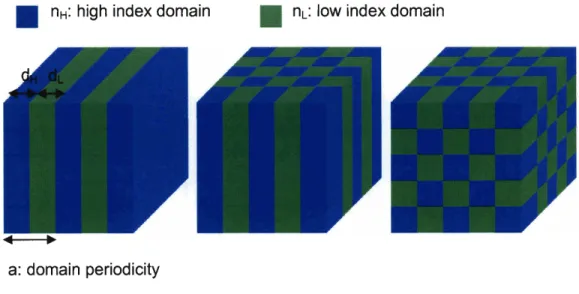
n ~ : high index domain n ~ : low index domain
a: domain periodicity
1 D Photonic Crystal 2D Photonic Crystal 3D Photonic Crystal Figure 1.1: A schematic diagram of ID, 2D, 3D periodic photonic crystals composed of high (blue) and low (green) refractive index domains. This diagram was adopted from [ 5 ] .
Besides these top-down lithographic approaches, bottom-up self-assembly methods have also been actively pursued for making photonic-bandgap structures. Synthetic opals made of spherical silica or polymeric colloidal particles have been extensively studied. 17'18 The closed-packed structures yield the face-centered cubic (FCC) structure or, after infiltration by a second material and removal of the original spheres, the inverse FCC struct~re.'~ More recently, block copolymers have emerged as alternative platform material for fabricating photonic crystals, because of their inherent flexibility in accessing a variety
of ID, 2D, and 3D periodic structures; their ability to incorporate a wide choice of materials including the possibility of high-dielectric and optically active nanoparticle additives; and their relatively straightforward, cost-effective processing methods.*'
1.2. ID, 2D, and 3D Block Copolymer Photonic Crystals
Photonic crystals will be an important part of future optical systems. For example, a discrete region of different index or geometry that serves to break the symmetry inside the photonic crystal can serve as an optical cavity, while a line defect can act as a waveguide and a surface defect can act like a mirror. As these features are all on the size scale of the wavelength of light, this affords both integration and miniaturization of optical devices. Even the most basic photonic crystal, a 1D multilayer stack in which the dielectric constant varies along only one direction, can act as a notch filter (a filter that can pass a narrow wavelength range of incident light) by incorporating a single defect layer in the stack. Multilayer devices are normally fabricated by various layer-by-layer approaches such as vacuum deposition, sputtering, co-extrusion, or spin-coating methods. Another way to produce 1D photonic crystals is by self-assembly of lamellar block copolymers.
Block copolymers, macromolecules comprising chemically distinct polymer chains covalently connected to each other, self-assemble to create a variety of periodic str~ctures.~' The self-assembly of block copolymers is driven by a competition between the positive enthalpy of mixing of the respective block chains and the tendency for the
polymers to desire a random coil configuration. When XN is larger than a certain value (e.g., 10.5 for symmetric diblocks), where
x
is the Flory-Huggins interaction parameter between blocks and N is the total degree of polymerization (equal to the total numbers of A monomers and B monomers) of the block copolymer, microphase separation into well- defined domain structures occurs on the length scale of the respective blocks. For example, in the case of simple linear A-B diblock copolymers, the volume fractionf
and XN determine the four equilibrium morphologies: lamellae, double gyroid networks, hexagonally packed cylinders, and body-centered cubic (BCC) spheres, as schematically shown in Figure 1.2. The diversity of block copolymer microstructures in terms of microdomain size and shape is greatly increased by changing the number of components, the architecture, the persistence length (a measure of the local straightness of the polymer chain) of the constituting chains, or by blending with additives (homopolymers, plasticizers, etc.). For example, A-B-C terpolymers, in which three chemically different blocks are either connected in a series via two junctions or connected to a single junction to form miktoarm ("mixed arm" in Greek) star polymers, exhibit a range of more complex morphologies compared with simple diblock copolymers.22 The wide range of microstructures accessible from the self-assembly of block copolymers has made them excellent candidate materials for numerous nanotechnological applications, including photonic-bandgap materials. 20,23Block copolymers of typical molecular weight (- 50 kglmol) form microdomains on a typical length scale (- 20 nrn) that is insufficient for optical applications. What is needed in order to produce a bandgap at visible or near-IR wavelengths is to increase the average
domain size to on the order of W4ni, where ni is the index of refraction of the respective block and h is the wavelength of light. For 600 nm visible (red) light, and for a typical
polymer index of 1.5, this calls for an individual block layer thickness of approximately 100 nm, requiring a block molecular weight of -500 kglmol and a total polymer molecular weight of around 1,000 kg/mol. Such large domain spacings can also be accessed by employing somewhat lower-molecular-weight copolymers (e.g., -200 kg/mol per block) and swelling the respective domains by blending with low-molecular-weight homopolymers or nonvolatile plasticizers, or by employing rigid, rodlike polymers with a large persistence length.
Figure 1.2: .A schematic diagram showing various bulk morphologies of linear diblock copolymer, poly(A-b-B), as a h c t i o n of volume fraction of A block (The double diamond bicontinuous
network structure does not occur for simple diblocks). This diagram was adopted from Dr. Banita
Dair
.
I
Nature of patterns Space group Blue domains: A block Volume fraction of A blockSpheres Cylinders Double gyroid Double diamond Lamellae (SPH) (3D) (CYL) (2D) (DG) (3D) (DD) (3D) (LAM) (1 D)
1m5m ~ 6 m m 1a?d ~ n ? m Pm
fg
17
2Figure 1.3: ID, 2D, 3D photonic crystals from (a) lamellar (from [26]) (b) cylindrical (from [32]) and (c) double gyroid (from [36]) morphologies of PS-b-PI block copolymers, respectively. Figure 1.3(a) is a TEM image of an Os04 stained PS-b-PI diblock, Figure 1.3(b) is an AFM image of cylindrical PS-bPI diblock, Figure 1.3 (c) is a SEM image of ozone-etched double gyroid PS-b-PI diblock.
The first example of a visible block copolymer photonic crystal was achieved by using a symmetric poly(styrene-b-isoprene) (PS-b-PI) diblock copolymer with approximate molecular weights of 200 kglmol per block and forming a 60120120 ternary blend with the respective homopolymer of each block. 24, 25 Indeed, the systematic blending of low- molecular-weight homopolymers into the host block copolymer provides a way to open the photonic bandgap (the so called "stop band") across the entire visible wavelength range by
simply controlling the amount of blended h ~ m o ~ o l y m e r s . ~ ~ More recently, block copolymers based on readily available olefins were developed to construct self-assembled photonic crystals of improved thermal stability and processability. Random copolymerization of olefm monomers provided a route to tune the refractive index of each block as well as to suppress the crystallinity for optical transparency. This work was in
collaboration with Dr. Robert Mathers and Prof. Geoffrey Coates at Cornell University (see appendix). Some examples of block copolymer based ID, 2D, 3D photonic crystals are depicted in Figure 1.3.
A convenient way to understand the optical properties of a photonic crystal is to examine the dispersion relationship between the frequency o and the direction of the wave vector k of incident light. If we consider an infinite periodic medium, the w(k) relationship can be derived from solutions to Maxwell's equations and is displayed as a band diagram.27 The dispersion relationship of a 1D photonic crystal has been also analytically derived by Yeh et a1.28 Figure 1.4 is an illustration of the band diagram for a multilayer system with layer thicknesses and refractive indices illustrative of 1D photonic crystal of a lamellar- forming PS-b-PI block copolymer, and provides information on sample reflectivity as a function of incidence angle and polarization of the incident electromagnetic waves. 29, 30 The areas between the first band (blue) and the second band (red) and above the third (red) band on the diagram represent propagating modes, while the areas between the second and the third band represent the nonpropagating evanescent modes. Light in this range of wavelengths incident for the particular kll vector (a projected k vector parallel to the interface between two domains) is reflected by constructive interference from the set of periodically spaced interfaces between the two types of domain. The plot also shows how the center wavelength of the bandgap is shifted to a shorter wavelength (or a higher frequency) as the incidence angle moves from normal (kll = 0 ) toward grazing (light line). Thus, a film appearing green when viewed at normal incidence appears blue when viewed at an angle far off the normal.
Figure 1.4: A band diagram (dimensionless frequency vs. dimensionless wavevector) using the refractive indices of polystyrene (rips = 1.59) and polyisoprene (npI = 1.5 1) and the layer thicknesses of a PS-b-PI block copolymer (dps = dpI = 100 nm). The transverseelectric (TE) polarization modes are on the right side, and the left side is for the transverse-magnetic (TM) polarized light. The numerical code was written by Dr. Martin Maldovan at MIT. (c: speed of light in a vacuum, a: lamellar domain periodicity = dPS+dPI)
A second way to understand the same sort of reflectance data for afinite photonic
crystal, which is more experimentally relevant, is to plot the magnitude of the reflectivity
(this depends on the dielectric contrast ( E ~ / E ~ ) and, importantly, on the number of periods in
the photonic crystal) as a h c t i o n of polarization, wavelength, and incident angle of light as shown in Figure 1.5. This type of calculation can be done using the transfer matrix method3', which also allows one to include finite material absorption in the calculation as
Incidence Angle
(deg.)
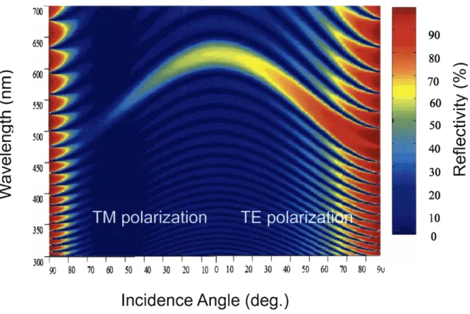
Figure 1.5: Reflectivity plot constructed by the transfer matrix method for a 20-period stack of alternating PS (n = 1.59) and PI (n = 1.5 1) layers (glass substrate-(PS layer-PI layer)20-air), for TM (left) and TE polarization (right), respectively. Each layer is assumed to be 100 nrn thick. The color represents the strength of the reflectivity at a particular polarization, frequency, and angle of incidence of incident light.
Two-dimensionally periodic block copolymer photonic crystals have been also demonstrated using self-assembly. In this case, a cylinder-forming PS-b-PI diblock copolymer was roll-cast to realize a long-range-ordered 2D periodic photonic crystal structure.32 The bandgap exists in the plane of the domain periodicity; thus, light
(-1.1) in the PSIPI material produced only a partial photonic bandgap. In order to achieve a complete bandgap for both transverse-electric (TE) and transverse-magnetic (TM) polarizations in the hexagonal cylinder structure, a minimum dielectric contrast of 7.2: 1 is necessary. This illustrates the challenge to somehow access a much higher dielectric contrast than is inherent to polymeric systems.
A three-dimensionally periodic photonic crystal with a complete photonic bandgap in the optical or near-IR frequencies has been one of the main challenges for researchers since the inception of the field in 1987. Yablonovitch first proposed that a FCC arrangement of dielectric cubes would provide the sought-after complete bandgap.33 Researchers attempted to create such a FCC photonic crystal structure using close-packed spheres, but the bandgap occurs at a relatively low volume fraction of dielectric, so infiltration of a high dielectric material about a template of FCC packed spheres, followed by etching to create an air lattice of spheres in a high dielectric was done.19 Unfortunately, the FCC structure does not have a complete bandgap between low-order bands, and the complete gap opens up between the eighth and ninth bands only at a relatively large dielectric contrast of nearly 9: 1 .34 Since then, researchers have sought alternative structures that would provide a robust gap at a lower dielectric contrast that could also be readily fabricated. Interestingly, the current champion photonic-crystal structure is that of an interconnected diamond network first discovered by the Iowa State University group in 1991 .35 The 19 vol % diamond dielectric network displays a complete bandgap between the second and third bands at the record low dielectric contrast of 3.6:l (note: attaining an
index contrast of 1.9: 1 in a diamond network structure is not out of the question for po1ymer:air structures).
Block polymers can provide many possible intricate 3D structures through microphase separation. The first 3D block copolymer photonic crystal having a partial photonic bandgap was based on the bicontinuous double gyroid cubic morphology.36 Here a PS-b-PI block copolymer with total molecular weight of 750 kglmol provided domain sizes sufficient to interact with visible light.36 The double gyroid morphology was fiuther treated with W and ozone to degrade the polyisoprene phase, leaving the polystyrene double gyroid network with increased refractive-index contrast (polystyrene versus air, 1.6: 1, see Figure 1 . 3 ( ~ ) ) . ~ ~
However, it turns out that the double gyroid network structure does not possess a complete gap, no matter how high the dielectric contrast. This makes clear the need to perform simulations of potential structures to explore for robust bandgaps prior to undertaking extensive experiments. The Thomas group at MIT have used numerical calculations employing the plane wave method34 to examine a host of network structures having various cubic symmetries.37 What is done is to systematically explore the range of volume fractions and dielectric contrasts for a given structure to see if it displays a complete gap and then to construct a "gap map9'-that is, a plot of the width of the complete gap (the difference in frequency of the lowest frequency of the upper band and the highest frequency of the lower band versus dielectric contrast at a fixed volume fraction). Of particular concern is finding the structure and the volume fraction of the structure at which a complete gap first opens at the lowest possible dielectric contrast. This
volume fraction will give the widest gap for a given dielectric contrast. It is noteworthy that neither the double gyroid nor the double diamond structures exhibit complete bandgaps, while both of the corresponding single network structures do, with the single diamond network as the current champion complete gap structure. The single gyroid morphology is also a quite favorable photonic crystal structure-a complete photonic bandgap opens at a index contrast of 2.3: 1 .37
1.3. Nanocomposite Block Copolymer Photonic Materials
Given the inherently low refractive index contrast (n21nl) in block copolymer-based photonic crystals (typically on the order of 1.1 : 1 for po1ymer:polymer structures and 1.5 : 1 for po1ymer:air structures) it is essential to enhance the index contrast in order to produce a more robust (or even complete) photonic bandgap. One method that has been successllly demonstrated is to selectively sequester high-refractive-index inorganic nanocrystals into the microdomains of a block copolymer to form an inorganiclorganic microstructured nanocomposite photonic structure. For example, CdSe particles with trioctyl phosphine oxide (TOPO) surface ligands (CdSe refractive index, -2.7) were successllly sequestered into the poly(viny1 pyridine) domains in a poly(styrene-b-isoprene-b-vinyl pyridine) block terpolymer.24~ 29 In order to target the high-index nanoparticles to the higher-index block domains, one needs to tailor the nanocrystal surface to have compatibilizing groups (typically oligomeric homopolymers) similar to the host block domains. Thus, mine- or
thiol-terminated polystyrene was used to compatibilize CdSe nanocrystals into PS-b-PI block copolymers by ligand-exchange reactions. Since the electronic bandgap of semiconductor nanocrystals is inversely proportional to the size of the nanocrystals, the absorption band of nanocrystals is shifted to a shorter wavelength than in bulk materials, making the nanocrystals effectively transparent in the optical regime.
Metallic nanoparticles are also of interest for their extremely high dielectric constants. The optical response of block copolyrner/metallodielectric nanocrystal photonic structures can be dramatically influenced by the spatial distribution of metallodielectric nanocrystals because of the dipolar coupling between closely spaced metal particles. For example, a metallodielectric photonic structure based on poly(styrene-b- ethylenelpropylene) diblock copolymer and gold nanocrystals was coassembled using gold nanocrystals with a size well below the scattering limit.38' 39 The gold particles were surface-grafted with different chemical groups, such as thiol-terminated oligomeric polystyrene or thiol-terminated alkanes, to target a given type of microdomain in the block copolymer template. Two distinct spatial distributions of gold nanocrystals were observed: (1) interfacial segregation between the two block domains, or (2) preferential uniform distribution within one type of domain. These morphologies were dependent on the surface chemistry and size of the ligands attached to the particles.40 The confinement of the nanocrystals to the narrow interface between domains results in a high local particle concentration and therefore a small average distance between particles, leading to different optical properties of the respective nanocomposite structures.40
Thermodynamic prediction of block copolymer-nanoparticle phase diagrams is thus of importance in designing nanocomposites for applications. Balazs' group has combined density hctional theory and self-consistent field theory to simulate the behavior of nanoparticles of diameter d in block copolymer domains of period L. They showed that the interfacial segregation of nanoparticles with neutral ligands (i.e.,
x
= 0) occurs for small particles (dlL < 0.2)' whereas for dlL-
0.3, the particles locate in the center of the domain4'.39,43
42, which was in reasonable agreement with experiments as well. There are a host of parameters to explore concerning the localization of particles within block copolymer microdomains. These include the particle size and shape, ligand size and chemistry, and the size and shape of the particular host micr0domain.4~ Information about the solubility limits of various particles in block copolymers is the key in understanding the attainable limits to the effective dielectric constant via blending. Clearly, there is much still to be done to control the hierarchical structures in block copolymer-nanoparticle assemblies that can enhance nanocomposite photonic properties.
1.4. Switchable BCP Photonics
Block copolymer-based photonic-bandgap materials that can be readily tuned or switched by applying various external fields can provide a route to fabricate multifunctional and optically responsive photonic structures. There is a host of ways to induce changes of
optical properties via alteration of the periodicity, symmetry, or dielectric constants of the material.
Thermally tunable block copolymer-based photonic-bandgap materials have been constructed by incorporating guest liquid-crystalline molecules into one domain of host block copolymers by hydrogen-bonding interaction to form a hierarchical photonic structure. Either the effective refractive index45 or the lattice spacing46 of liquid-crystal- containing domains could be changed as the temperature of the materials was changed, leading to the tailoring of the position and strength of the photonic stop band of the system.
Another way to alter the microdomain spacing in a block copolymer is to apply mechanical force. Elastomeric block copolymer photonic crystals have been prepared by blending with a nonvolatile plasticizer to form a block copolymer gel. The local deformation of the photonic gel's microstructure yields a tunable photonic bandgap with applied tensile strains.30
Recently, chemically, thermally, mechanically responsive self-assembled reflectors based on PS-b-PI block copolymer solution have been nicely demonstrated and will be presented in Chapter 5 of this thesis.
1.5. Challenges, Advantages, and Applications
In order to maximize the usefdness of self-assembled block copolymer platforms, one has to address three major challenges: attaining large domain spacings, achieving high
dielectric contrast, and controlling long-range microdomain order. The occurrence of randomly located defects that accompany the self-assembly process must be avoided. In this regard, there have been numerous efforts to establish a single-crystal-like microdomain structure, employing various extemal fields such as mechanical flow fields, electric fields, temperature gradients, directional solidification, and surface interactions to obtain purposefully long-range domain order during the self-assembly process. However, the very high molecular weight block copolymers that are typical of photonic crystals presents the problem that the order4isorder transition is unattainable via temperature, so that solvents must be used to process the materials into their final structures, restricting the applicability of some of these techniques.
Advantages for employing self-assembled block copolymers as visible wavelength photonic materials include the ease of processing (e.g. conformal coating on essentially any substrate); the ability to incorporate both inorganic (e.g. quantum dots) and organic additives (e.g. laser dyes, liquid crystals, homopolymers, and plasticizers, etc.) within the block copolymer microdomains; and the relatively easy manipulation of block copolymer microstructures via various extemal fields such as mechanical force, temperature, and electric fields, etc.
As mentioned in the introduction, attainment of well-ordered photonic crystals is only a necessary requirement. Actual useful optical devices need controlled defects to localize and guide light. One interesting application is the use of the self-assembled block copolymer photonic crystal to define a microcavity for modifying the spontaneous emission of optically active materials, ultimately leading to an optically pumped, all-organic, self-
![Figure 1.3: ID, 2D, 3D photonic crystals from (a) lamellar (from [26]) (b) cylindrical (from [32]) and (c) double gyroid (from [36]) morphologies of PS-b-PI block copolymers, respectively](https://thumb-eu.123doks.com/thumbv2/123doknet/14170033.474446/28.918.143.819.191.396/figure-photonic-crystals-lamellar-cylindrical-morphologies-copolymers-respectively.webp)