RESEARCH OUTPUTS / RÉSULTATS DE RECHERCHE
Author(s) - Auteur(s) :
Publication date - Date de publication :
Permanent link - Permalien :
Rights / License - Licence de droit d’auteur :
Institutional Repository - Research Portal
Dépôt Institutionnel - Portail de la Recherche
researchportal.unamur.be
University of NamurEmissive and cooling properties of carbon based materials for microelectronics
Miskovsky, Nicholas; Cutler, Paul; Mayer, Alexandre; Lerner, Peter
Published in: Cold Cathodes II
Publication date: 2002
Document Version
Publisher's PDF, also known as Version of record
Link to publication
Citation for pulished version (HARVARD):
Miskovsky, N, Cutler, P, Mayer, A & Lerner, P 2002, Emissive and cooling properties of carbon based materials for microelectronics. in M Cahay, KL Jensen, PD Mumford, VT Binh, C Holl & JD Lee (eds), Cold Cathodes II. vol. 2002-18, pp. 175-210.
General rights
Copyright and moral rights for the publications made accessible in the public portal are retained by the authors and/or other copyright owners and it is a condition of accessing publications that users recognise and abide by the legal requirements associated with these rights. • Users may download and print one copy of any publication from the public portal for the purpose of private study or research. • You may not further distribute the material or use it for any profit-making activity or commercial gain
• You may freely distribute the URL identifying the publication in the public portal ? Take down policy
If you believe that this document breaches copyright please contact us providing details, and we will remove access to the work immediately and investigate your claim.
Emissive and Cooling Properties of Carbon Based Materials for Microelectronics
N. M. Miskovsky, P. H. Cutler, A. Mayera, and Peter B. Lerner Department of Physics
104 Davey Laboratory The Pennsylvania State University
University Park, PA 16802
ABSTRACT
Among carbon-based materials, diamond and nanotubes exhibit field emission characteristics, which can be very useful for applications. These include low extraction field, high current density and long operating time. In general, the emission features of these materials exhibit Fowler-Nordheim type current-voltage characteristics. Such characteristics generally are associated with tunneling but may also be due to a non-tunneling mechanism. This is exhibited in our study of field emission from wide band gap metal-semiconductor nanocomposites. In these latter materials, the grains of the wide band gap semiconductor are embedded into a layer of metal. Interfacial charge transfer gives rise to metal-induced gap states (MIGS) in the vicinity of the grains. If the density of the semiconductor grains is sufficiently large, MIGS hybridize with conduction band states of the semiconductor forming a quasi-band, which can be populated by the electrons from the metallic matrix through the scattering in the metal-semiconductor composite. The location of the high-lying MIGS in the vicinity of the conduction band of the wide bandgap semiconductor (e.g., diamond) significantly reduces the barrier between those states and the vacuum level compared to the work function of a metal. Thus low-threshold field emission from a nanocomposite becomes possible. This hypothesis is supported by Monte Carlo simulations of transport through a nanocomposite.
The authors have also formulated a simple quantitative theory of microelectronic cooling by field emission from thin film composite devices. This involves a three-step process of “hot” electron injection, transport, and vacuum emission. Significant cooling from these devices, even including metallic emitters, is feasible because of a corrected theory of the electron replacement process in the Nottingham effect. This is briefly reviewed and macroscopic cooling results are presented for temperatures from above ambient to cryogenic.
To study field emission from both metallic and semiconducting nanotubes, Mayer and Vigneron [ A. Mayer and J.-P. Vigneron, “Real-space formulation of the quantum-mechanical elastic diffusion under n-fold axially symmetric forces,” Phys. Rev. B 56, 12599 (1997)] developed a scattering formalism, which goes beyond the simplified one-dimensional kinetic treatment used by Fowler and Nordheim and most subsequent analyses. The transfer- matrix methodology used here incorporates three-dimensional aspects of the atomic structure as well as the field emission tunneling process. Using this formalism, the authors have investigated the following: field emission and FEED from metallic (5,5) and semiconducting (10,0) capped and open single walled nanotubes (SWNT), the effect of absorbates on field emission and FEED from SWNT, field emission from multi-walled nanotubes (MWNT), and other properties. These results will be briefly reviewed.
a Permanent address: Laboratoire de Physique du Solide, Facultes Universitaires N.-D. de la Paix, Rue de
I. Field Emission from Nanocomposites
One of the principal objectives in electron field emission sources is to provide low threshold emission (LTFE). Two of the first groups who demonstrated this effect are Geis et al. [1] and Okano et al. [2]. There is an intriguing connection between LTFE and the roughness of the surface of metal-semiconductor contacts in field emission elucidated in a number of theoretical and experimental works [3-10]. In this review we describe a model for achieving LTFE through the use of nanocomposites, i.e., a metallic matrix with embedded grains of wide band gap semiconductors, e.g., diamond or GaN. Field emission from these materials has been studied since the mid-eighties [6] and more recently interest in nanocomposites has resurfaced in connection with light-emitting devices [4,5].
For an ideal field emitter one must combine electron field acceleration with relatively low thresholds for emission. This is feasible in vacuum or the conduction band of dielectrics, but is less efficient in metals or the valence band of dielectrics. Thus, a desirable field emitter is a composite device combining a source of electrons (e.g., metal or highly n-doped semiconductor) and subsequent acceleration in vacuum or a dielectric. In Ref. [4] the authors prepared a gold matrix containing the particles of GaN and AlN on the order of 3-8 nm in size. In Fig. 1a, we show schematically the band structure for the grain embedded in the metal matrix. The Fermi level of the semiconductor equilibrates with the energy on the Fermi surface of the metal. The height of the barrier between field electron states in the metal and the conduction band of an un-doped semiconductor has a magnitude of half the band gap (~1.7 eV for GaN, ~2.7 eV for diamond, and ~3.1 eV for AlN) which is comparable to the work function of metals and does not give a significant lowering of the field emission threshold. However, because of the small size of the grains one cannot consider the semiconductor lattice as well as the surrounding metal to be strictly periodic. Violation of periodicity manifests itself in the states inside the band gap of the semiconductor, which are pinned to the metal-semiconductor interface and are called metal-induced gap states (MIGS) [9]. Close to the edge of the band gap the wave function for the MIGS are localized but with a tail extending up to 100 Å. If the semiconductor particles are about this size and the average distance between them is about the same, the wave functions of the MIGS can either overlap or hybridize among themselves and with the conduction-band states of the semiconductor (Fig. 1b). Thus the concept of individual MIGS pinned to a particular grain loses its validity. We describe the emerging structure as a quasi-band, which is approximately pinned to the edge of the conduction band of the semiconductor. If an NEA face of the wide band gap semiconductor granule is close to the vacuum-composite interface, field emission from this quasi-band becomes possible at a very low threshold because there is essentially no barrier between these states and vacuum. The quasi-band is formed near the bottom of the conduction band of the semiconductor. If this band can be populated, then electron emission from this band is possible at low fields for NEA or small PEA materials. We describe a method for population of such a band.
(a)
(b)
Fig. 1 Band structure for the grain embedded into the metal matrix.
a. Band structure of an isolated grain with metal-induced gap states (MIGS). No band bending is shown.
b. Hybridization of MIGS in multiple grains. Band bending is shown.
The quasi-band states are not populated under equilibrium conditions. Indeed, the states that can be populated are located close to the Fermi level of the metal, which is approximately in the middle of the semiconductor band gap. They have small localization length, do not hybridize and have approximately the same field emission threshold as the surrounding metal. If we apply an electric field across a nanocomposite, the resulting near-equilibrium electrons in the metal can be scattered by stray electric fields that are present inside the semiconductor. These fields appear as a consequence of the interfacial charge transfer as well as the external field applied to the layer of the nanocomposite. If the scattering in the grain, whose size is typically comparable to 10 nm, is sufficient to extend the energy tail of the electron distribution to 2-3 eV, the quasi-band may become populated giving rise to significant field emission from the surface of the nanocomposite. We emphasize that, in principle, inelastic absorption of phonons and
plasmons can contribute to a broadening of the energy distribution on the high energy side. However, as has been shown in simulation studies by the authors of phonon and plasmon scattering, the main contribution to the energy broadening in the tail of the distribution is due to elastic scattering by electrons [8]. This occurs through a series of billiard-type collisions in which random energy losses are continuously replenished by the external electric field so that field energy gains can accumulate[8].
To prove that broadening can occur, we have done a simulation using our Monte Carlo code [10]. Because there are grain boundaries in the semiconductor film, there is an additional type of scattering to be considered. This represents the fact that we really have a metal-semiconductor composite and electrons (which emerge with thermal energy) can scatter strongly at the boundary of the grain. This scattering is modeled by alloy scattering in which we represent a metallic fraction of the composite by a fictitious alloy component with a significant difference of an analogous electron affinity.
Electron-alloy scattering has been considered by Harrison and Hauser with application to ternary III-V compounds of the form AxB1-xC [11]. Their model described
the alloy component as a "square-well" potential barrier with the magnitude corresponding to the difference between electron affinities of components A and B. However, their model (which uses a truncated form of the 1st Born approximation) predicts unlimited growth of the scattering rate with energy, which rapidly approaches 1016 s-1 for a reasonable (several eV) difference in electron affinities and for energies in the tail of the electron distributions (i.e., hot electrons with energies ~ eV). This unbounded scattering rate is obviously unphysical because the scattering should diminish when electron energy exceeds the height of the barrier. Moreover, their result does not depend on the size of the scatterer, r0.
The scattering rate given by Harrison and Hauser [11], has been derived on the assumption that the change in wavevector (∆K) associated with a momentum change satisfies the relationship ∆Kr0<<1 [11]. This is unjustified in two cases: 1) the scatterer is
large, 2) electron energies are much larger than kBT. In our case, where scatterers are
grains of mesoscopic size rather than atomic impurities and the typical electron energies are in the eV range, neither of these conditions holds. Thus, we must use the scattering rate that results from a full untruncated first Born amplitude, which, to the authors’ knowledge, has not been derived for this case of alloy scattering. After some algebra, the following formula is obtained:
0 0 * 2 2 2 ) / 2 ( ) )( 1 ( 3 r v r E m f E C C Pe−alloy = π A − A ∆ε h e (1) where ) cos( ) sin( ) ( x x x x f = − , (2)
and, CA is a fraction of component A, ve is the velocity of an electron with effective mass m*, N is the electron particle concentration in a unit volume, and ∆ε is a difference in electron affinity between components A and B.
In contrast to the results of Harrison and Hauser [11], the rate given by the new result in Eq. (1) is bounded. For the energies much higher than ∆E, the rate diminishes with energy as ε-3/2. Although the first Born approximation is not applicable in the narrow range of electron energies around ∆ε, this does not affect the results of the
out because this narrow range of energies constitute a small fraction of the phase space volume.
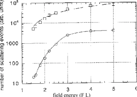
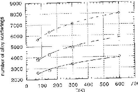
To quantify this picture we performed Monte Carlo simulations of the acceleration in a microscopic grain. We present, in Fig. 2, the growth of the scattering in a diamond nanocrystallite as a function of field. The grain scattering is the dominant type of scattering. It grows monotonically with the temperature and is roughly proportional to T1/5 (Fig. 3) and increases with the alloy fraction. The extension of the tail of the hot electron distribution is shown in Fig. 4. For Ei >EG/2, where Ei is the energy of a
particular stimulated electron and EG is the band gap, a population of charge carriers in
the quasi-band occurs. For the case of NEA, or low PEA, of the diamond surfaces, we may, to first order, identify the current density from the quasi-band with the field emission from the sample.
field energy (F L)
Fig. 2 Growth of the number of scatterings with field energy E = (F.L). L is here identified with the particle size r0. The upper curve corresponds to the total number of scatterings associated with all e-e, e-phonon, and e-alloy scattering processes. The lower curve corresponds to the number of scatterings associated with the e-alloy scattering process.
Fig. 3 Temperature dependence of alloy scattering in the range 75-600 K. Curves correspond to different concentrations: solid (x=0.04), long dash (x=0.1) and short dash (x=0.4), respectively.
Fig. 4 Concentration dependence of maximum energy (solid) and most probable energy (dash). Bars indicate the average width at half-maximum. The temperature T=300K.
I.1 Non-Tunneling Field Emission Current
We note that in the case of hot electron propagation the mobility and the diffusion coefficient are not related anymore by the Einstein relation, D=kBTµ/e, because the short-range electron propagation is not diffusive, but quasi-ballistic [8]. These coefficients constitute two independent characteristics of the electron propagation. Thus, we evaluate the I-V characteristics of the nanocomposite by calculating the fluctuation currents (which are ~ D) which are most directly related to the loss of electrons from the sample.
One distinguishes between the fluctuation current through the grain (which is indicative of the ohmic conductivity of the film),
∑
∆∆ ∝ i i i tot xt j 2 (3)and the fluctuation current in the band, which is assumed to be,
∑
> ∆ ∆ ∝ 2 / 2 ) ( G i E E i i i band xt E j ρ . (4)In Eq. (6), we define the density of states in the quasi-band by 2 / ) (Ei = A Ei−EG ρ (5) with 1 2 / ) ( − > =
∑
G i E E i E A ρ . (6)Here ∆xi=xi-<xi> is the instantaneous displacement from the average in the time interval ∆ti , the elapsed time for the electron to cross the grain.
I.3 Results
The fluctuation band current is plotted in Fig. 5. This current is now identified with the field emission current, because we consider escape into vacuum as barrier-free. As expected, the current through the band becomes significant when the field energy exceeds the energy gap between the Fermi level of the semiconductor and the bottom of the conduction band with Fr
band
j
0>EG/2. While the current jtot is ohmic with jtot~V, the band current jband has a highly nonlinear dependence on the applied bias voltage. In Fowler-Nordheim coordinates, the plot of jband(V) is approximately a straight line. We must emphasize that the origin of the "field emission" in this case has nothing in common with conventional field emission via tunneling. This new mechanism is, basically, the acceleration of quasi-free electrons of the weakly conducting nanocomposite film by the stray fields produced by an external bias on the edges of the semiconducting grain. Because of the presence of the wide band gap semiconductor with NEA or small PEA on some of its surfaces, a fraction of the more energetic electrons are emitted into vacuum instead of losing their energy in the metal. In contrast to conventional field emission, in this case the energy of the emitted electrons in vacuum is rather small.
1/V
Fig. 5 Plot of the band current in Fowler-Nordheim coordinates, at T=300K
In Fig. 6, we can deduce an important relationship between electron-alloy scattering and the high-energy tails of the energy distribution. We observe that about ~40% of electrons are promoted to the quasi-band for r0=300Å. We identify with this number an approximate grain size threshold for emission which we define as the field energy for which ~50% of electrons are promoted to the quasi-band due to the increased electron-alloy scattering.
Fig. 6 Dependence of the number of scattering events into the band (E>EG/2) on the grain size. Maximum and the width of the energy distribution are plotted on the secondary axis.
The electrons with sufficiently high energy to enter the quasi-band states can escape into vacuum without impediment (i.e., there is a small effective barrier). In Fig. 5, we are tempted, as in a conventional FN plot, to determine the work function from the slope of the analogous FN plot of the nanocomposite. This is, however, spurious because the energy parameter obtained from the slope of the I-V curve plotted in FN coordinates in Fig. 5 cannot be identified with the usual work function parameter in conventional tunneling field emission.
In Fig. 7 we demonstrate the dependence of the mobility in the sample on temperature in the range 75K<T<600K. We note that the mobility falls with increasing temperature, according to the approximate power law: µ=A(Fr0)T0.15, independent of whether the field energy is near, above or below the threshold for field emission. This is due to the fact that most phonon emission rates increase with increasing temperature. However, the temperature dependence of the diffusion coefficient D~jtot is not monotonic (see Fig. 8). It increases with the temperature below the threshold, decreases above the threshold and exhibits irregular behavior near the threshold. We speculate, that this may happen because of the interplay of the electron-alloy scattering, which is temperature independent and the electron phonon scattering, which becomes more efficient with energy. The overall behavior varies as T1/5 because electrons, with increased alloy scattering, tend to spend more time in the crystal and can therefore lose energy by other possible mechanisms. For smaller accelerations (or shorter samples), the diffusion-stimulating effect of elastic scattering overtakes diffusion-limiting effect of energy losses through emission of phonons and plasmons. For higher net energies (longer samples), energy losses tend to dominate.
Fig. 7 Electron mobility as a function of temperature. Solid line corresponds to below threshold case (r0 = 250 Å, Fr0=2.5 eV), long dash, to the threshold case (r0 = 300 Å, Fr0=3 eV) and the short dash—to the above-threshold case (r0 = 400 Å, Fr0=4 eV).
Fig. 8. Temperature dependence of the effective diffusion coefficient kBTµ (arb. units). Solid line corresponds to r0=250 Å, long dash—to r0 = 300 Å, and the short dash to r0 = 400 Å.
I.2 Conclusions: Nanocomposites
In this study, we have proposed a non-tunneling field-emission mechanism for nanocomposites which is an alternative to electron injection interfacial tunneling. This process has been described qualitatively by Geis [1] and Okano et al. [2], and treated quantitatively by Lerner et al. [12]. This mechanism is based on the hybridization of the MIGS with the states of the conduction band of the grains of the wide band gap semiconductor and subsequent acceleration of the quasi-free electrons by high electric fields, which are generated at the nanocrystals as the result of interfacial charge transfer and the applied electric field. It is suggested that this mechanism is responsible for the observed phenomena of low-threshold emission from the heterogeneous CVD diamond films as well as observed low field acceleration of the electrons emitted from Mo tips electrophoretically coated by powder-like diamond [13,14].
In reality, both mechanisms (that is, tunneling between conduction bands of the metal and wide band gap semiconductor and stray-field acceleration ) may co-exist in a single composite cold cathode emitter. It is important to note that the interband internal field emission is independent of temperature because all the characteristic energy parameters are much larger that kBT. By contrast, the acceleration by the stray fields and
subsequent scattering depends upon temperature through the phonon scattering rates and the grain scattering (~T1/5).
Another verifiable prediction of the present model is the energy spectrum. The stray-field induced field emission of the type described above is a relatively low energy process, which results in a broadened energy distribution. On the other hand, the elastic tunneling mechanism produces a narrow peak close to the field energy. Ideally, this should provide a way to distinguish between a tunneling and the non-tunneling stray field process. In practice, however, the independent measurement of the voltage drops in different layers of the composite emitter and in the vacuum region (between the film and anode) is difficult to obtain. Hence, distinguishing between these types of emission by examining the energy spectrum may not be feasible, and is a challenge to be addressed.
Finally, we illustrate in Table 1 that the low threshold field predicted for this new field emission mechanism is achieved with a low β-factor. In this table we summarize some estimates of the local threshold fields associated with different field emission processes. These values are obtained from model calculations of the I-V characteristics for each mechanism [8,12,15, 16]. It is important to note that in the case of internal field emission through a Schottky barrier, there are two contributions to the total (local) field, one is due to the charge transfer producing the Schottky barrier and the second is due to the applied field, which is the one listed in the table. One can then determine the β-factor for each process, which is required to produce field emission at low threshold macroscopic fields. As seen in Table 1, such a low threshold field is predicted for the non-tunneling stray-field mechanism proposed in this paper.
Table 1. Comparison of the calculated local threshold fields for different emission mechanisms. The field enhancement factor is estimated so as to provide the necessary local fields to initiate field emission at low macroscopic applied fields.
Type of Field Emission Local Threshold
Field (V/Å) Field Enhancement Factor (β) Metal-Vacuum Tunneling (few) x 0.1 ~1000
Internal Field Emission [M(S)] through a Schottky Barrier
(5-6) x 0.01 ~100
Stray-Field Acceleration in
a 15 nm Grain 2 x 0.01 30-50
II. New Analysis and Results of Microelectronic Cooling Using the Nottingham Effect in Field Emission.
One of the main limitations in the development of more dense and smaller microelectronic devices is the problem of removal of heat to limit the temperature increase due to Joule heating (e.g., in Si or GaAs technology, Tmax≤50ºC, with heat
dissipation ~ 1-5W/cm2). By heat dissipation or cooling we mean maintaining a given microelectronic device at a predetermined steady state operating temperature. For other applications, the cooling capacities required range from fractions of a watt to as much as 10 watts at operating temperatures that vary from cryogenic to ambient and above. There are also a significant number of applications that require fractional watt cooling capacities at very low temperatures (<10 K). Today, the two main cooler technologies are (i) mechanical coolers, and (ii) electronic coolers based on the Peltier effect. Electronic coolers associated with Peltier or thermoelectric coolers are commonly used for electronic chip cooling and even small portable commercial coolers. However, they produce only a moderate amount of cooling and have limited efficiency, due to the fact that the hot and cold junctions are thermally connected with the p and n type semiconductors. The efficiency also drops significantly as the temperature difference between the hot and cold junctions increases [17,18].
In the past, some of the proposed solutions to this problem are [17]:
• Thermoelectric devices. Bi2Te3 and other exotic materials show promise but
• Thermionic cathodes. They operate at relatively high temperatures and to-date have not been realized as practical coolers [17]. Below we describe a thermionic cooling device proposed by Mahan, which uses periodic barriers in a multi-layer geometry [19].
• Conventional Nottingham Coolers. Field emission into vacuum can cool cathodes but practical application was impeded by incorrect analysis of energy exchange process and choice of materials [20-22].
• Resonant Tunneling. Korotkov and Likharev have proposed possible cooling based on resonant tunneling in a planar thin-film structure using a-few-nm-thick wide-band gap semiconductor [23]. Green and Tsu [21] have also proposed cooling devices based on resonant tunneling. Although the resonant type of electronic cooler is very promising, it faces formidable fabrication challenges [21,23]
• Narrow bandgap p-type inverse Nottingham coolers. Figure of merit may be larger than thermoelectrics, but there is no practical device as yet. Tsu and Greene have proposed an inverse Nottingham cooler using a narrow bandgap p-type semiconductor [21]. For these cooler devices, the figure of merit may be larger than thermoelectrics. However, finding materials with requisite properties and difficulty in fabricating such a device has impeded development [23].
• Microjets, embedded heat pipes, etc., discussed in detail in reference 17.
We will restrict the analysis to thermionic and field emission cooling processes. We begin with a brief description of a proposal by Mahan for thermionic refrigeration. This illustrates the essential physics and material requirements for thermionic cooling. We will then briefly review the early studies on the feasibility of Nottingham cooling by field emission.
Mahan proposed a thermionic refrigerator process using N arrays of thermionic emitters [18]. This approach is illustrated below using the potential energy diagram by Mahan [18].
The multi-step thermionic emission process involves 1) electrons ballistically emitted over the barrier with thermalization in each successive electrode. This results in a small temperature and voltage drop per barrier. To obtain a coefficient of performance (or efficiency) of ~1 requires materials with work functions of ~ 10 meV, which to date have not been realized for practical application. Another approach using thermionic emission was proposed by others [24].
The use of a field emission process for refrigeration was first proposed by Levine [25] who did a model calculation of a vacuum field emission device operating as a “heat pump.” He computed the maximum rate of heat flow as a function of emitter temperature using the Fowler-Nordheim model and the classical heat transport equations. Rates in excess of 0.1 cal/s/cm2 [0.42 W/cm2] was predicted at room temperature if the emitter work function is less than 1 eV. The sensitive dependence of the cooling rate on the work function is not a consequence of Fowler-Nordheim theory but is a general result because of the important role of the tunneling barrier in this problem. It is important to note that the requirement for a low work function material was predicted on the original but erroneous assumption that the average value of the energy of the replacement electron entering the metallic emitter was equal to the Fermi energy. Furthermore, since the corrected theory of the replacement energy predicts values up to ~ 500 meV [26,27], extrapolation of Levine’s [25] and Brodie’s [20] calculations on Nottingham cooling in conventional metallic field emitters predicts very appreciable cooling rates.
We have recently proposed a new approach for an efficient, compact, low power consumption electronic cooler designed for applications in microelectronics, and operating from cryogenic to ambient and higher temperatures. The new paradigm involves cooling via electron field emission from diamond or III-nitride thin films deposited on metal or silicon substrates. This new cooler concept is based on the Nottingham effect, according to which electrons emitted from a cathode can, under optimized conditions, leave with an average energy greater than that of the replacement electrons, resulting in the cooling of the emitter [26]. As the electrons reach the other electrode (typically the anode), heat is transferred from the cathode to the anode. If the anode is thermally isolated from the cathode, the process leads to an efficient heat pump. The authors have previously shown that composite diamond films can be used to develop viable electronic coolers for a range of temperatures above ambient [27], with macroscopic cooling rates that range up to hundreds of W/cm2 depending upon the average energy of the replacement electrons, temperature and density of emitters on the metal substrate.
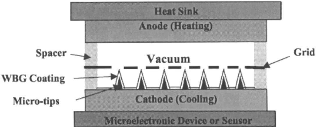
II.2 Model of Cooler
A schematic of a proposed cooling device is given in figure 9. The theory of operation of this device has already been described in detail by the authors in References 27, 35-37. The cooling or the energy exchange process begins with the absorption of heat from the "hot" source into the electron gas of the metal, with the subsequent transfer of these hot electrons from the metal into diamond by tunneling through the Schottky barrier, and their transport (ballistically or quasi-ballistically) through the diamond across a vacuum interface to a heat sink, where their energy is degraded. (Energy degradation in the heat sink can be done, for example, by using retarding potentials., with the subsequent removal of heat by radiation and convection processes.) Because of the ballistic transport, the heat carried by the electrons is essentially decoupled from the lattice and back flow to the device is minimal. With NEA or small positive electron affinity surfaces, the electrons can be emitted from the diamond film with little or no power for electron emission.
Fig. 9. Schematic of an integrated composite metal(S)/N-doped Diamond(WBG) thin film device for microelectronics cooling. Essentially, heat is injected through a thermal conductor (electrical insulator) into the substrate(cathode) producing an excited electron gas. After tunneling through the interface region (Micro-tips/WBG coating), these “hot” electrons are transported (ballistically or quasi-ballistically through the WBG coating)and emitted into the vacuum and then strike the anode which is in contact with the heat sink.
II.3 Energy Exchange in Field Emission
We describe here briefly the energy exchange process in field emission and how Nottingham inversion leads to a cooling process. Field emission is the quantum mechanical tunneling of electrons through the surface barrier produced by an applied electric field. During the process of field emission, energy exchanges take place between the emitted electrons and the cathode surface [25-35]. In addition, energy transfers between the replacement electrons from the external circuit and the cathode lattice become important at the electron densities present in field and thermal-field emission. If the average energy <εe> of the emitted electrons is less than that of the replacement
electrons, <εr>, the cathode tends to be heated during the emission. If <εe> is greater than
<εr>, the cathode tends to be cooled as predicted by Nottingham [28]. For emission at T =
0 K, all the energy states above the Fermi energy are empty. Hence, all emitted electrons have less energy than the Fermi energy. For T> 0 K, the higher levels become populated and contribute preferentially to the emission, causing an increase in the average heat removed per emitted electron. In most calculations of the Nottingham effect which use the conventional or classical theory, the energy of the replacement electron has been taken to be, under equilibrium conditions, the Fermi energy, εF, equal to the chemical
potential µ (this is the average value of the replacement energy proposed by Nottingham in 1941 [28]). Under steady state conditions for each electron emitted from a cathode, a replacement electron is supplied to the system from the external wire. In this dynamic exchange, energy states in the emitter are vacated by thermal excitation or tunneling and are reoccupied by electrons supplied from the external reservoir. A schematic diagram of the process for a metallic emitter is shown in Fig. 10. The replacement energy is a statistical average of the vacant states into which replacement electrons can be scattered. For example, some of the replacement electrons absorb thermal energy from the lattice and are excited into the energy states above the Fermi level. Using statistical mechanical analysis, Chung et al. [22] calculated the average energy of the replacement electrons, extending the suggestions by Fleming and Henderson [29] that one must take into
results in a value of <εr> less than εF by an amount, which, in general, exceeds several
hundred meV. This corrected value of the replacement energy significantly enhances the cooling rates [27].
Fig. 10. Schematic of field emission tunneling and replacement process. For simplicity, not all states that can tunnel are depicted as doing so. Furthermore, some states are depicted as empty because of thermal excitation.
II.4 Model Calculations of the Cooling Rate
Using the kinetic formulation for field emission, it can be shown that the power/area carried by the emitted current relative to the average energy of the replacement electrons from the external circuit, <εr>, is:
dW W D dE E f m E H a W r ( ) ( ) 2 ) ( 0 3 2
∫ ∫
∞ ∞ − > < − = h π ε (7)where W is the normal kinetic energy, -Wa denotes the bottom of the band, and all other
symbols have their usual meaning.
The WKB transmission coefficient, D(W), is
∫ + + + − − = 2 1 2 / 1 ) 0 ( 4 2 2 2 2 exp ) ( z z dz tic electrosta V z z e F E W m W D κ h (8)
where the quantum modified image potential is used and Velectrostatic is a Schottky barrier
consisting of the depletion layer charge contribution and the applied fields. The quantity κ is the dielectric constant of diamond. Using Eq. (8), H is,
dW z z dz tic electrosta V z z e F E W m dE E f m E H a W r ∫ + + + − − × > < − =
∫ ∫
∞ ∞ − 2 1 2 / 1 ) 0 ( 4 2 2 2 2 exp ) ( 2 ) ( 0 3 2 κ π ε h h . (9)The details of the determination of the Schottky barrier for a model spherical pointed tip are given in References 16-18. To obtain the potential barrier, the solution of the radial Poisson equation is obtained subject to the appropriate boundary conditions in the barrier region. It is important to note that the cooling rates determined by equation (9) are a function of temperature, and the geometry of the device through the transmission coefficient. By selecting an appropriate portion of the band structure and using the geometry-dependent potential barrier, a filtering effect is obtained which enhances the cooling rates by restricting the tunneling of electrons from states below the Fermi energy [35-37].
II.5 Calculated Cooling Rates
Calculations of the cooling rates have been done as a function of applied voltage across the device and the tip radius for a fixed Nitrogen-doping density (taken to be 1019/cm3) in the diamond film. All other electronic and physical parameters are the same as in Ref. [27]. Figs. 11 and 12 depict the local cooling rates (i.e., the cooling rates at the apices of the tips) for T=500 K, as a function of applied voltage with values of the replacement energy ranging from 25 meV to 100 meV below the Fermi energy. Using the same formalism, cooling rates can be calculated for any temperature in this range and down to 10 K and below. The radius of curvature of the spherical metallic tip is taken to be Rt=10
nm, a relatively sharp tip. Results for cooling rates in a temperature range from ambient to cryogenic (i.e., T=100K) using a blunt tip (i.e., Rt=50 nm) are presented in Ref. [38].
It can be seen from Ref. 38 that the local cooling rates at all temperatures are appreciable even for the relatively small corrections to the replacement energy, <εr > used above, the
choice of which tends to set lower bounds to the cooling rates. As expected, the cooling rates are a function of temperature. The higher the temperature, the larger the population of electrons in higher energy states and, hence, the larger the amount of energy removed per electron by the emitted electrons.
Calculations also show that the maximum cooling rates are a strong function of the tip radius, yielding larger local rates at lower voltages (lower power) for smaller values of R. This is due to the fact that the local field is enhanced for sharp tips and falls off rapidly with distance, preferentially thinning the barrier for electrons in the higher energy states compared to electrons below the Fermi energy. As the radius of curvature increases, the field is more uniform, and this preferential thinning is reduced, leading to a reduction in the tunneling current. In Figure 13, the local cooling rates are shown as a function of Rt with the replacement energy taken as equal to the Fermi energy (i.e., the
Fig. 11. The local cooling rate per area for a single tip as a function of applied voltage (across the device to be cooled) for different values of <εr>=εF-∆εr. Curves (C)-(F) correspond to values of ∆εr=25,50,75, and 100 meV, respectively. The temperature, T=500K, and the radius of curvature Rt=10 nm.
Fig. 12. An expanded view of the curves for the local cooling rate per area for a single tip as a function of applied voltage (across the device to be cooled) for different values of <εr>=εF-∆εr. In this graph we only show curves (C)-(D), which correspond to values of ∆εr=25,50 meV, respectively. The temperature, T=500K, and the radius of curvature Rt=10 nm.
Fig. 13. The local cooling rate per area for a single tip as a function of applied voltage (across the device to be cooled) for different values of radius of curvature of the tip. The average replacement energy, <εr>=εF. The temperature is T=500K.
It is important to note that it is the cooling rate averaged over the macroscopic area that is experimentally accessible and of practical interest. This is the product of the local cooling rate/area, the effective area per tip, and the tip density. In the calculations presented here, the tip is taken to be a hemisphere, where the effective area is determined by assuming that the actual emission is concentrated in a cone of about half angle 10º centered on the apex [39]. However, we have chosen a half-angle of 20º because a more recent analysis indicates that these estimates of the local angular current dispersion may be on the conservative side [40]. The resultant diminution of the current per tip reduces the cooling rates. The adjusted macroscopic cooling rates are presented in Table I for the radius of curvature of the tip of 50 nm. In the calculations we have continued to use relatively conservative values for the corrections to the replacement energy. The cooling rates are a strong function of this parameter and would be orders of magnitude larger for values between 300 and 500 meV which are predicted in our calculations. This is dramatically illustrated by noting that at T=500 K, the cooling rates for ∆εr=0 and 100
meV differ by 3 orders of magnitude. Similar results are evident for T=100 K when ∆εr
Table I. The adjusted macroscopic cooling rates for different values of the replacement energy <εr>=εF- ∆εr, with Rt=50nm, and a tip density of 107/cm2.
Temperature K ∆εr meV 0 25 50 75 100 1000 H W/cm2 13.0 23.7 43.5 80.0 145 500 H W/cm2 1.24x10 -3 8.41x10⁻³ 5.73x10⁻² 0.333 1.64 300 H mW/cm2 1.19x10 -5 1.47x10⁻³ 1.51x10⁻¹ 5.85 102 100 H mW/cm2 _______ _______ _______ 0.119 10.4
II.6 EFFICIENCY OF A COOLING DEVICE
For completeness we briefly describe the ideal efficiency of such a device. The operational definition of the cooling efficiency is given by [17,19]:
V J J P H input power time removed heat Qh in = ∆ = = . / . η (10)
where JQh is the heat current/area or rate of energy removal/area from the system, J is the
electrical current density, and ∆V is the applied voltage. We note that Eq. (10) is equivalent to the coefficient of performance of a refrigerator. Hence, it can be used to determine the cooling efficiency of either a hot body (i.e., removing heat from a hot body and transferring it to a heat sink) or a cold body (i.e., a refrigerator or “heat pump”). For the case of a Carnot refrigerator, which involves the heat removal from a cold body, Eq. (10) reduces to: T T T T T P H input power time removed heat h c h h in = − = ∆ = = . / . η (11)
where Th and Tc refer to the temperatures of the hot and cold reservoirs, respectively. It is
worth noting that a high efficiency for a Carnot refrigerator does not necessarily imply large cooling rates. In fact, cooling rates may be small, if the value of ∆T is small.
For a thermoelectric cooler , JQh is given by, T
K STJ
JQh = − ∆ (12)
where S is the Seebeck coefficient, T the absolute temperature, and ∆T is the temperature difference between the hot and cold “reservoirs.” In order to take into account the heat currents in the pure field emission process, the heat current equation must include the Nottingham exchange process, which takes into account explicitly the energy difference between the tunneling (or emitted) electrons and the replacement electrons. Then the analogous form of Eq. (12) for the field emission case is
< >−< > = e J JFE e r Qh ε ε . (13)
Physically, Eq. (13) is the flux density of the heat carrying electrons times the average energy exchange per electron. Thus, using Eq. (10) the cooling efficiency (or coefficient of performance) for the Nottingham effect is:
∆ > < − > < = V e r e FE ε ε η (14)
This is interpreted as the heat removed per electron divided by the work done on an electron by the battery.
To achieve high cooling efficiencies, the device should be operated at low T and low voltage. This is due to the fact that at low temperatures, there is a small population of electrons above the Fermi energy and most of the tunneling current comes from electrons near the Fermi level. As the voltage is increased, states lower in energy contribute more to the tunneling current. For all temperatures, as the voltage is increased beyond a certain value, the barrier is thinned sufficiently so that significant numbers of electrons are emitted from states well below the Fermi energy. At some voltage, the average energy of the emitted electrons is less than that of the replacement electrons and the cathode is heated.
To estimate the efficiency, we refer to Fig. 13 which shows the local cooling rates as a function of tip radius with the classical Nottingham replacement energy, <εr>=εF.
(Recall that this represents a lower bound on the cooling rates.) Since the maximum cooling rate shifts to lower applied voltages as the radius of curvature of the tip decreases, the efficiency increases with decreasing tip radius. As we have indicated, the corrected value of the replacement energy can be several hundred meV or more less than the Fermi energy. Then the energy exchange in Eq. (14) can be up to 500 meV or greater (at fields in the field emission range, i.e., F~0.2-0.7 V/Å). For an applied voltage of ∆V~1V, the efficiency ηFE≥0.5 or 50%. This number corresponds to a value of ZT≥1.3
for thermoelectrics, values which have not yet been achieved for practical thermoelectric devices.
These initial studies suggest cooling rates which can meet the requirements of thermal management for current microelectronic technology. Thus, refinement of the theory and modeling of Nottingham coolers (both field emission and thermionic) seem warranted. This will involve a corrected statistical mechanical theory of Nottingham cooling in both narrow and wide band gap semiconductors. In addition, detailed analysis of electrical and heat transport must be done to account for the additional energy exchanges due to Joule heating, radiation, and convection. The ultimate goal is to determine the feasibility of applying the Nottingham cooling paradigm to cryogenic temperatures of less than 100 K, where device heat removal requirements can be significantly less than milliwatts.
III. Study of Field Emission, Transport, and Band Structure Using the Transfer-Matrix Scattering Formalism
III.1 Introduction
Among carbon-based materials, diamond and nanotubes exhibit field emission characteristics, which can be very useful for applications. These include low extraction field, high current density and long operating time [41-43]. In general, the current voltage characteristics of the nanotubes follow a Fowler-Nordheim type tunneling law. To study field emission from both metallic and semiconducting nanotubes, Mayer et al. [44-46] have developed a scattering formalism, which goes beyond the simplified
one-dimensional kinetic treatment used by Fowler and Nordheim and most subsequent analyses. By contrast, Mayer et al. [44-46] used a transfer- matrix formalism which incorporates three dimensional aspects of the atomic structure and the field emission tunneling process. Using this formalism, they have investigated field emission and FEED from metallic (5,5) and semiconducting (10,0) capped and open single walled nanotubes (SWNT) [47-49], the effect of absorbates on field emission and FEED from SWNT [50], field emission from multi-walled nanotubes (MWNT) [51], and other properties involving radiation [52,53]. These results will be briefly reviewed in light of application as high current, low voltage electron sources.
III.2 Theory
The geometry considered in this paper is depicted in Fig. 14. The nanotube is located between a metallic substrate (Region I, z§ -Na) and the field-free vacuum (Region III, z¥ D). The intermediate region consists of a field-free region -Na§z§0, which contains N periodic repetitions of a basic unit of the nanotube, and Region II 0§z§D), which contains the part of the nanotube subject to the extraction field. This field results from an electric bias V that is established between the two limits of Region II. The periodic repetition of N basic units of the nanotube in a region preceding that containing the extraction field reproduces appropriate band structure effects in the energy distributions. Due to the nanometric dimensions of both the nanotube and the cathode-anode distance D used in our simulations, the applied electric field V/D (which is in the order of a few volts per nanometer here) should be regarded as a local field, i.e. already magnified by a micron-long nanotube body, in order to account for experimental fields being typically of a few volts per micron.
Fig.14. Schematic diagram of the geometry of the nanotube field emission process. Region I (z≤-aN) is a perfect metal. The intermediate region, -a N≤z≤0, contains N repetitions of a basic unit of the (5,5) nanotube. Regions II, 0≤z≤D, contains the part of the nanotube subject to the electric field. Region III, z>D, is the field-free vacuum region. The arrows in the Regions I and III symbolize the scattering solutions, with a single incident state in Region I and the corresponding reflected and transmitted states (whose coefficients are contained in the transfer matrices t-+ and t++, respectively).
The potential energy in Region II is calculated by using techniques of Ref. [53], with a pseudopotential for the ion-core potential (the expression given in Ref. [53] for the l=1 states). This choice of the l=1 pseudopotential is justified by the fact that the electronic properties associated with the transport of current in nanotubes essentially come from π-orbitals. The electronic density associated with the four valence electrons of each carbon atom are represented here by the sum of two Gaussian distributions (whose parameters are given in Ref. [49]). These electronic densities are displaced from the nuclear positions according to the polarization of the corresponding carbon atom. The dipoles pj are calculated [47] by taking account of the extraction field, dipole-dipole
interactions and the anisotropic polarizability [46] of the carbon atoms. The electronic exchange energy is evaluated by using the Local Density Approximation 43CXρ1/3,
whereρ is the local electronic density and
( )
3 1/30 2 4 3 4πε π e CX =− .
To compute electron scattering from the metallic substrate (Region I) to the vacuum (Region III) taking account of three-dimensional aspects of the potential barrier in the intermediate regions, we used the transfer-matrix technique developed in previous publications [44-46]. In this formulation, the electrons involved in the transport remain localized inside a cylinder of radius R in the regions preceding the vacuum Region III (R is chosen large enough so the field-emission results are independent of its particular value). The wave function is expanded in terms of basis states in Region I as
) ) ( exp( ) exp( ) , ( , 22 , , , Am jJm km j im i m E Vmet z I j m = ± − Ψ ± h ϕ ρ in region I and ) exp( ) exp( ) , ( , 22 , , , Am jJm km j im i mED D j m = ± h
Ψ ± ρ ϕ in the anode plane z=D,
where the are normalization coefficients, are Bessel functions, are transverse wave vectors which are solutions of ,
j m A , Jm , , j m j m k , 0 ) (k R =
Jm E is the electron energy and is the potential energy in the supporting metal. The signs refer to the propagation direction relative to the z-axis, which is oriented from the Region I to the Region III. The transfer-matrix methodology then provides scattering solutions for the reflected states Ψ and transmitted states corresponding to a single incident state from the metal Ψ (see Fig. 14 for a schematic representation). Total current densities result from the contribution of all solutions associated with propagating incident states in the supporting metal. The two structures considered in this work are the armchair (5,5) metallic and zigzag (10,0) semiconducting nanotubes.
met V ± − , , I j m + , , j − , , D j m Ψ I m
To obtain a representation of the bandstructure of the (5,5) carbon nanotube, we determine the combinations of basis states whose value is preserved (except for a multiplicative factor C) after propagation through a basic unit of the nanotube. The combinations for which |C|=1 correspond to propagative states. If a is the length in the z-direction of the basic unit, the permitted wave vector values kzfor a given energy E are solutions of C =eikzz (the restriction of
z
k between –π/a to +π/a is automatic). For a given problem, this technique provides a particular representation of the band structure, since its complex three-dimensional structure is projected on the kzaxis. This is a consequence of solving the problem of the propagation of a wave function in
three-components (through the use of basis functions for the representation of the transverse behavior of the wave function). [47] The present technique is, however, appropriate to the study of carbon nanotubes, since band structures are usually represented according to the same kz coordinate.
The band structure for the (5,5) nanotube is given in Fig. 15. The permitted kz values are displayed horizontally for each value of the energy E. These energy values are relative to the Fermi level, whose position is fixed from the middle of the metallic plateau region presented in Fig. 16. The Fermi energy is determined to be 5.25 eV below the vacuum level (which corresponds to the highest energy represented in the figure).
Fig. 15. Representation of the band structure of a (5,5) carbon nanotube. Each point is associated with a combination of basis states, which is merely multiplied by a factor
after propagation through a basic unit of the nanotube (whose length a=0.246 nm).
a ikz
e
The two horizontal lines in Fig. 15 delineate the range of energies (from –2 to 0.2 eV relative to the Fermi level), which are considered in the simulations of the field emission.
The band structure is typically that of a metal. As expected, the number of bands increase as the energy approaches the vacuum level, where the states are more representative of freely propagating electrons. Near the Fermi energy the bands are linear with discontinuities, which affect the total-energy distributions that will be discussed later. This linear behavior is interrupted when the distance in energy from the Fermi level exceeds 1.4 eV as then new bands appear, thus marking the limits of the metallic plateau region presented in Fig. 16.
We note that our calculated band structure does not exhibit the distinctive feature of crossing at the Fermi energy, which is exhibited in tight-binding calculations. Our calculation of the band structure differs from the tight-binding calculations [54] in that it uses a scattering formalism with the tested Bachelet pseudopotential and the local density approximation.
We plot in Fig. 16 the total-energy distribution of electrons in the plane z=0. The supply function is determined by the free-electron metal in Region I (which for the purpose of reflecting the properties of an infinite nanotube, is given the same work
function of 5.25 eV). To enable the states with energy higher that the Fermi level µ to be visible in the figure, the Fermi-Dirac exponential damping factor is not included although it is taken into account in the field emission simulations. The three curves correspond to N=16, 32, and 64 periodic repetitions of a basic unit of the nanotube between the supporting metal in Region I and the plane z=0. The central metallic plateau ends approximately at 1eV on both sides of the Fermi level. There are oscillations in the energy distributions whose number increases proportionally to the number N of basic units. These oscillations are the result of standing waves. It is expected that the number of oscillations increases with the length of the nanotube and indeed the calculations predict this. For a 16-nm long nanotube (64 basic units), they are typically 0.2 eV apart in the vicinity of the Fermi level. The discontinuities in the band structure of Fig. 15 are reflected by irregularities in the energy distributions, which are more pronounced at – 1.55, -1.4, 10.75, 0.12, 1.1, and 1.25 eV relative to the Fermi level. At this last value, a number of new bands appears in the band structure so the number of states in the total-energy distribution grows proportionally. The fact that only two branches associated with propagative solutions exist at the Fermi level may explain why field emission beams obtained experimentally from a variety of nanotubes exhibit strong angular dependence.
Fig. 16. Total energy distribution of incident states at z=0 for N=16 (solid), 32 (dashed), and 64 (dot-dashed) periodic repetitions of a basic unit of the (5,5) carbon nanotube.
The total-energy distributions of the incident and transmitted states are illustrated in Fig. 17. The four curves correspond to the incident distribution at z=0 (where the Fermi-Dirac distribution factor is now included) and to the transmitted distributions at z=D for applied fields of 2., 2.5, and 3 V/nm. The distribution of incident states exhibits a sharp peak at the edge of the metallic plateau, which is related to the van Hove singularity [54] associated with the closure of a band at –1.4 eV relative to the Fermi level (See the bands denoted by arrows in Fig. 15). The discontinuities in the band structure also explain the irregularities observed at –1.55 and –0.75 eV in the energy distribution. The other oscillations in the distributions come from standing waves in the nanotube (i.e., those already observed in Fig. 16).
When plotted in Fowler-Nordheim coordinates, the current characteristics gives approximately a straight line, whose slope indicates a field enhancement factor of 3.8 comparable with the small aspect ratio [L/D≈2.5] of the part of the nanotube subject to the field in our model. Considering a micron-long body would meet both experimental
values of the enhancement factor that is typically between 500 and 800 for multi-wall nanotubes [42] and around 3000 and above for single-wall nanotubes [41] and experimental values of the extraction field [55].
To study the field emission from a semiconducting (10,0) carbon nanotube, we used the same transfer-matrix formalism and model described above. The geometry is the same as in Fig. 14, except for the position of the atoms. It is well known from tight-binding models [56] and recent calculations by Mayer et al. [48] that the electronic states of the (10,0) nanotube are characterized by a gap in its energy distribution. This gap appears clearly after only a few repetitions of a basic unit of the nanotube, as can be observed by studying the energy distribution of states in the plane z=0 as the number N of these basic units is progressively increased.
Fig.17. Normalized total-energy distribution for an open (5,5) nanotube of the incident states at z=0 (solid) and ot the transmitted states at z=D for applied fields of 2 (dashed), 2.5 (dot-dashed) and 3 V/nm (dotted) The mximal values are respectively 0.23x10⁻³, 0.11x10⁻⁹, 0.87x10⁻⁷, and 0.81x10⁻⁶ A/eV, respectively.
To illustrate this fact, we plot in Fig. 18 the total-energy distribution of electrons in the plane z=0, after propagation through N=16, 32, and 64 basic units of the nanotube. The sharpness of the gap is a consequence of all states being evanescent in this energy range. The energies are relative to the Fermi level, which for an intrinsic case is at the middle of the gap 5.7 eV below the vacuum level.
Fig.18. Total energy distribution of incident states at z=0 for N=16 (solid), 32 (dashed), 64 (dot-dashed) periodic repetitions of a basic unit of the (10,0) carbon nanotube.
The gap is well pronounced for the three values of N used in Fig. 18 and its width is approximately 1.35 eV. The deepening of the gap increases with the number N of basic units. The two sharp peaks at the edges of the gap in Fig. 18 are due to the van Hove singularity associated with the closure or opening of bands [54]. As with the (5,5) nanotube, the oscillations are related to standing waves that appear in the N units of the nanotube at given energy values. The number of these oscillations is expected to increase with the length of the nanotube and indeed the calculations predict this.
For the study of field emission, we now focus on the total-energy of the electrons arriving at the anode at z=D. The extraction field results from an electric bias of 12 V, which is established between the planes z=0 and z=D (anode, see Fig. 14). Different values of the field are obtained by changing the distance D. For these simulations, the field-free region z≤0 includes N=16 units of the (10,0) carbon nanotube (i.e., 640 carbon atoms), which are connected to 4 units (i.e., 160 carbon atoms) in the region z≥0 where the extraction field is present. The first and last atoms in this region are located respectively at z=0.071 and 1.633 nm (relative to the plane z=0 separating the parts of the nanotube inside and outside the field region). The tube radius is 0.381 nm.
The total-energy distributions of the field-emitted electrons are presented in Fig. 19. The three curves correspond to applied electric fields of 2, 2.5, and 3 V/nm. The total-energy distribution of electrons in the plane z=0 is reproduced for comparison.
Fig.19. Normalized total-energy distribution for an open (10,0) nanotube of the incident states at z=0 (solid) and othe transmitted states at z=D for an applied electric field of 2 (dashed), 2.5 (dot-dashed), and 3 V/nm (dotted). The maximal values are 0.15x10⁻³, 0.40x10⁻¹⁹, 0.17x10⁻¹⁷, and 0.37x10⁻¹³, respectively.
The peak associated with a van Hove singularity at the edge of the gap and the gap itself are at a fixed position for all field values. This constant position is a consequence of the band structure effects responsible for the gap and the van Hove singularity being calculated in the field-free region z≤0.
The unnormalized values as well as the width of the distributions associated with the transmitted states increase with the extraction field, in agreement with elementary field-emission theories [39]. When plotted in Fowler-Nordheim coordinates, the current characteristics give approximately a straight line, whose slope indicates [1] a field enhancement factor of 2.5 consistent with the small aspect ration (L/D≈2.5) of the part of the nanotube subject to the field in our model. As in the case of the metallic (5,5) nanotube, considering a micron-long body would meet both experimental values of the field enhancement that is typically between 500 and 800 for multiwall nanotubes [41] and around 3000 and above for single-wall nanotubes [42] and experimental values of the extraction field [55].
Using the same methodology, we have also done three-dimensional calculations of field electron energy distributions from open hydrogen-saturated and capped metallic (5,5) carbon nanotubes. The total-energy distributions calculated for the open hydrogen-saturated structure are illustrated in Fig. 20. The four curves correspond to the incident distribution at z=0 and the transmitted distributions at z=D for local electric fields of 2, 2.5, and 3 V/nm. These fields should be considered as already amplified by a micron-long body to account for the difference by 3 orders of magnitude with fields applied macroscopically [57]. The sharp peak at the edge of the metallic plateau in the distribution of incident states is due to a van Hove singularity [54]. The other oscillations are related to standing waves in the structure. The separation between these oscillations is inversely proportional to the length of the nanotube and is typically 0.2 eV in the vicinity of the Fermi level for a 16 nm long nanotube (64 basic units instead of 16 here).
Fig.20. Normalized total-energy distribution for an open hydrogen-saturated (5,5) carbon nanotube of the incident states at z=0 (solid) and ot the transmitted states at z=D for an applied electric field of 2 (circles), 2.5 (triangles) and 3 V/nm (squares). The maximal values are 0.23x10⁻³, 0.14x10⁻⁷, 0.11x10⁻⁴, and 0.77x10⁻⁴A/eV, respectively.
The total-energy distributions obtained with the closed (5,5) nanotube are present in Fig. 21, where the distribution of incident states is again comparted with those of the transmitted states when the local field is 2, 2.5, and 3 V/nm, respectively. The peak distributions are essentially similar to those obtained with the open structure (the overlap of peaks at 3 V/nm is, however, avoided here). These results thus illustrate the dominance of the part of the nanotube supporting the apex (on which depends the supply function of electrons facing the field region). There is however a sharp additional peak (which appears clearly in the curve associated with the 3 V/nm electric field 0.3 eV below the Fermi level). This peak can be interpreted as the result of a resonant-tunneling process [58] through the atoms of the half-C60 cap. The field enhancement factor derived
from the Fowler-Nordheim plot is 3.7, i.e., slightly larger than the previous 3.4 value and consistent with the higher aspect ratio.
Fig. 21. Normalized total-energy distribution for a closed (5,5) carbon nanotube of the incident states at z=0 (solid) and ot the transmitted states at z=D for an applied electric field of 2 (circles), 2.5 (triangles) and 3 V/nm (squares). The maximal values are 0.23x10⁻³, 0.57x10⁻¹¹, 0.27x10⁻⁸, and 0.39x10⁻⁷A/eV, respectively.
These results can be compared with those obtained with an ideal open (5,5) structure (i.e., without hydrogen saturation) 9210. The conclusions are that currents
than those obtained from the closed structure and that hydrogen saturation of the open structure multiply the extraction current by an additional factor of 200. Calculations by Adessi et al. [59] confirm that currents extracted from open structures are higher than from closed ones. Field penetration is one factor responsible for these current enhancements, since it reduces the height of the tunneling barrier. Field penetration is less pronounced in the closed structure, where the screening of the electric field is more efficient. However, the polarizability of hydrogen being smaller than for carbon, field penetration is more pronounced in the saturated structure. Another factor is the orientation of the polarization of the last atoms of the structure, which tends to reduce the thickness of the potential barrier when it is opposite to the direction of the field. For a carbon-hydrogen distance of 0.11 nm (value for methane) both the hydrogen and the last layer of carbon atoms are polarized opposite to the field, thus explaining this high enhancement factor of 200 (which is consistent with experimental observations [60] and hence led to the use of this value of 0.11 nm). Our results are strongly dependent on the carbon-hydrogen distance. Considering, for example, a value of 0.108 nm (value for benzene) results in an enhancement factor of only 3 (due to the last layer of carbon atoms being then oriented in the direction of the field). These transfer-matrix calculations of field emission from (5,5) carbon nanotubes thus strongly indicate that open hydrogen-saturated structures are better emitters than unhydrogen-saturated open or closed ones.
We also consider simulations of field emission from multi-wall nanotubes. The structures considered were the metallically ideal open single wall (5,5), (10,10), and (15,15) structures and the wall (5,5)@((10,10)@(15,15) nanotube. The two multi-wall structures considered were the flat and convex terminations shown in Figs. 22 and 23, respectively..
Fig. 22. Potential energy distribution (section in the xz-plane) corresponding to an opend (5,5)@(10,10)@(15,15) nanotube with flat termination, a cathode-anode spacing of 4.8 nm and a bias of 12 V.
Fig.23. Potential-energy distribution (section in the xz-plane) corresponding to an open (5,5)@(10,10)@(15,15) nanotube with convex termination, a cathode-anode distance of 4.8 nm and a bias of 12 V.
We first considered the single wall structures (5,5), (10,10) and (15,15). The total energy distributions of the electrons that are emitted from these structures are shown in Fig. 24. The distributions are similar and exhibit peaks at the same positions. These peaks are related to stationary waves in the structure. The fact that they appear at the same position is due to the fact that the three structures have the same length (and the same internal potential energy). The currents are respectively 0.298x10⁻⁷, 0.205x10⁻⁷, and 0.124x10⁻⁷ A. Considering that the radii are 1,2, and 3 times 0.339 nm, we see that the current extracted from these carbon nanotubes decreases with the radius and this decrease is essentially linear. This reduction of the current is due to the decrease of the field amplification factor as the radius increases, and aspect ratio decreases.
Fig.24 . Total-energy distribution of electrons field emitted from single-wall (5,5) (solid), (10,10) (dashed) and (15,15) (dot-dashed) nanotubes, respectively. The extraction field is 2.5 V/nm.