HAL Id: hal-02923017
https://hal.archives-ouvertes.fr/hal-02923017
Submitted on 26 Aug 2020
HAL is a multi-disciplinary open access archive for the deposit and dissemination of sci-entific research documents, whether they are pub-lished or not. The documents may come from teaching and research institutions in France or abroad, or from public or private research centers.
L’archive ouverte pluridisciplinaire HAL, est destinée au dépôt et à la diffusion de documents scientifiques de niveau recherche, publiés ou non, émanant des établissements d’enseignement et de recherche français ou étrangers, des laboratoires publics ou privés.
Nucleation and lateral growth kinetics of the NiSi phase
at the epitaxial θ-Ni2Si/Si interface
Mike El Kousseifi, Khalid Hoummada, Federico Panciera, Christian Lavoie,
Dominique Mangelinck
To cite this version:
Mike El Kousseifi, Khalid Hoummada, Federico Panciera, Christian Lavoie, Dominique Mangelinck. Nucleation and lateral growth kinetics of the NiSi phase at the epitaxial θ-Ni2Si/Si interface. Acta Materialia, Elsevier, 2020, 198, pp.100-110. �10.1016/j.actamat.2020.07.062�. �hal-02923017�
1
Nucleation and lateral growth kinetics of the NiSi phase at the epitaxial
-Ni
2Si/Si interface
M. El Kousseifi1, K. Hoummada1, F. Panciera1,†, C. Lavoie2, D. Mangelinck1*
1 IM2NP, Aix Marseille Université-CNRS, UMR 7334, Faculté de Saint Jérôme, 13397 Marseille, France 2 IBM Thomas J. Watson Research Center, Yorktown Heights, New York 10598, USA
†Current address: Université Paris-Saclay, CNRS, Centre de Nanosciences et de Nanotechnologies, 91120, Palaiseau, France.
Abstract
The first stages of the growth of the NiSi phase at the expense of θ-Ni2Si have been studied mainly by in-situ XRD measurements and atom probe tomography (APT) analysis. In-situ XRD isothermal annealing at different temperatures were performed on several samples in order to monitor the phase formation sequence, the time at which NiSi phase begin to form and its growth kinetics. These results show that while the phase formation sequence is the same, the time for the beginning of formation of NiSi varies from one sample to the other under the same isothermal temperature and experimental conditions. Comparing these findings with nucleation and growth models, the growth of the NiSi phase at the expense of θ-Ni2Si is controlled by nucleation compared to diffusion in the case of δ-Ni2Si as the first phase. The kinetics for the nucleation and lateral growth of the NiSi phase were deduced and the implications for the formation of this phase and for contacts are discussed.
Keywords: Nucleation; Thin film; Growth kinetics; In situ x ray diffraction; Nickel silicide
2
1. Introduction
Ni-based self-aligned silicides are widely used as contacts and interconnections in ultra-large-scale
integrated circuits [1]. They are obtained by a solid-state reaction between a Ni thin film and a Si
substrate. This reaction leads usually to the formation of δ-Ni2Si as the first phase followed by NiSi
after the complete consummation of Ni, and NiSi2 phase at higher temperature [2]. Among these, NiSi
is the phase of interest for its low resistivity as a contact material for CMOS devices. Despite its
advantages, NiSi suffers from severe agglomeration above 650°C and it transforms into the more
resistive NiSi2 phase above 800°C [3]. It has been demonstrated that the addition of a small amount of
alloying element to Ni film, such as Pt, Pd, Mo or Re, reduces the agglomeration of NiSi and prevents
its transformation into NiSi2 [4,5]. Therefore the addition of 5 at.% Pt was first used and the Pt
concentration has been increased in the Ni film from 5 at.% to 10 at.% for applications in
microelectronics [6–8]. The addition of alloy elements can modify the phase sequence and in particular
it has been observed that during the reaction of Ni (10 at.% Pt) with Si (100), θ-Ni2Si replaces δ-Ni2Si
as first phase [9]. In this case θ-Ni2Si grows in epitaxy with the Si substrate prior to the formation of
NiSi [10]. The composition of the intermixing layer formed at interface during deposition was found
to control the nature of the first phase and to lead either to -Ni2Si or -Ni2Si [11]. The growth of NiSi
at the expense of the δ-Ni2Si phase has been extensively studied with results showing that the NiSi
growth is controlled by diffusion of Ni as the fastest diffusion species [12–14]. In addition, it was
shown that there is a time delay between the formation of the NiSi phase and the end of the growth of δ-Ni2Si that was attributed to the strain relaxation in δ-Ni2Si phase. Furthermore, it was demonstrated
that this time delay follows Arrhenius behaviour with activation energy around 1.2 and 1.7 eV for pure
Ni and Ni(5 at.% Pt) respectively [15]. However, the growth of NiSi at the expense of θ-Ni2Si and
especially its first growth stages is not well understood. Indeed, in contrast to the extensive work concerning the growth of NiSi at the expense of δ-Ni2Si, only a few studies have been conducted to
3 epitaxial θ-Ni2Si/Si interface was evidenced by TEM [16]. The experimental shape of isolated NiSi
precipitates resulting from the lateral growth of NiSi at the θ-Ni2Si/Si interface was in accordance with
several models [16,17].
In this work, the nucleation and the lateral growth kinetics of NiSi phase at the epitaxial θ-Ni2Si/Si
interface have been investigated using in situ X-ray diffraction (XRD) and atom probe tomography
(APT) measurements. Several isothermal annealing (in-situ XRD) coupling with models have been
used in order to calculate the activation energy for NiSi nucleation and lateral growth kinetics.
2. Experimental
10-nm-thick Ni (10 at.% Pt) films were deposited by magnetron sputtering on (100) Si substrates. The
(100) Si substrates were cleaned with diluted HF prior to loading into the sputtering chamber. The
deposition was performed in a sputtering deposition setup with a base pressure of 10−8 Torr using a
99.99% pure Ar gas flow and a 99.99% Ni(Pt) target. The wafer was rotated during the deposition to
improve the homogeneity of the layer. Then, the reaction between the Ni(Pt) film and the substrate
was followed by in situ XRD. For XRD measurements, a Cu tube and a θ-θ geometry were used in a
a Panalytical X-Pert Pro MPD diffractometer. The samples were loaded into the XRD chamber (Anton
Paar TTK450), which is equipped with a heating stage and maintained under an ambient vacuum of
approximately 10−5 mbar. In the XRD chamber, the sample was hoeld by two stainless steel plates on
a metal block sitting on a heather and inside which a thermocouple was embedded. In situ isothermal
XRD analyses were performed by increasing the temperature from room temperature to the chosen
temperature at a rate of 30°C/min and by continuously recording the XRD spectra at this temperature
for a given time.
TEM measurements (TITAN microscope equipped with an image Cs-corrector and operated at 300 kV) were performed by cross-sectional views on samples prepared by a focused ion beam dual beam instrument (FIB, FEI Helios600 NanoLab) along the direction (110) of Si after deposition of a protection layer
4 The APT specimen preparation was performed using a Helios dual-beam Focused ion beam (FIB)
equipped with a micromanipulator and with a gas injection system (GIS) for Pt deposition. Several
steps are needed for the APT specimen preparation by FIB as described elsewhere [18,19]. The APT
analyses were carried out in a LEAP 3000X HR instrument. The laser pulsing rate was set at 100 kHz
and the detection rate was kept at 0.002 event/pulse by increasing the applied voltage. The samples
were analyzed under the following conditions: pressure in the range of 10-11 Torr, temperature of 25
K and laser energy of 0.5 nJ. These analysis conditions were applied to all the analyzed samples.
3. Results
Figure 1.a presents the in situ XRD measurement (intensity as a function of diffraction angle and time)
showing the phase formation sequence during an isothermal annealing at 215 °C for the 10 nm Ni(10
at.% Pt)/Si (100) sample. It can be summarized by the following. The consumption of the Ni(10 at.%
Pt) film (XRD peak at 44°) is associated to the formation of the θ-Ni2Si phase. θ-Ni2Si grows in epitaxy
with the Si substrate, which explains the absence of XRD peaks until the detection of NiSi phase [10].
Then, the formation of the textured NiSi phase (200) at the expense of θ-Ni2Si is observed with a single
XRD peak at 56.2°. From the in situ XRD data, the variation of the normalized integrated intensities
with time are reported for Ni consumption and NiSi formation in Figure 1.b (1st annealing). This
experiment was repeated several times under the same conditions (as deposited sample, atmosphere
and temperature) and the results are presented in Figure 1.b. The integrated intensity of a XRD peak
can be considered to be proportional to the volume of the corresponding phase in the absence of change
in the texture of the phase.
In all experiments at the nominal temperature of 215°C, the time for the complete Ni consumption (i.e. the formation of θ-Ni2Si) was found to be reproducible within a range of 50 min while the beginning
5 the NiSi phase is detected, the time to complete the NiSi growth is roughly the same showing that the
formation kinetics is roughly similar at the nominal temperature of 215°C.
Figure 1: In-situ XRD diagram (λ= 1.54 Å) during isothermal annealing at 215 °C on 10 nm Ni(10 at.% Pt)/Si(100) sample. (a) XRD intensities as a function of diffraction angle measured during the heat treatment (b) Variation of the
normalized integrated intensity of the XRD peaks as a function of time during four isothermal annealing at the same nominal temperature (215 °C).
Isothermal experiments at other temperatures (180, 200, 230, and 250 °C) have also been performed
in order to deduce the growth kinetic and to shed light on the variability of the start of NiSi formation.
Figure 2 shows the normalized integrated intensities of XRD peaks as a function of time for the Ni
consumption and NiSi formation during several isothermal annealing at 200 and 230 °C. The Ni
6 100 min at 200 °C, 50 min at 215 °C and 15 min at 230 °C. The beginning of the NiSi formation
appears to occur at different times for each isothermal annealing. The difference between the end of
Ni consumption and the beginning of NiSi formation will be now defined as the time delay for NiSi
formation. For example, at 230 °C, the time delay for NiSi formation varies between 2 and 75 min.
Figure 2: Results obtained by in-situ XRD diagram (λ= 1.54 Å) during two isothermal annealing on 10 nm Ni(10 at.% Pt)/Si(100) sample. The variation of the normalized intensity of the XRD peaks as a function of time after two isothermal
annealing a) at 200 °C and b) 230 °C.
From these results, the average time delay has been estimated for each temperature. This average time
delay decreases with temperature (~ 30 min for 230 °C, 150 min for 215 °C and 600 min for 200 °C).
It appears that with the temperature increase, the slope representing the growth of NiSi becomes steeper
which means that the growth kinetics has accelerated, as expected. We also notice that for a given
7 suggests that the variation in nucleation time could be due to a small difference in temperature between
different experiments. This hypothesis will be verified in the discussion.
In order to better understand the origin of these time delays, transmission electron microscopy (TEM)
and atom probe tomography (APT) have been used to characterize the nanostructure and composition
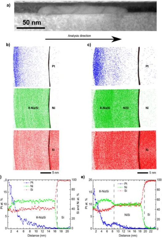
of the sample. Therefore, another in-situ XRD annealing at 215°C has been performed and stopped after the first appearance of the characteristic peak of NiSi at 2θ equal 56°. Then, TEM and APT were used after the annealing to characterize the sample. Figure 3.a is a TEM cross section showing a typical
NiSi precipitate at the θ-Ni2Si/Si(100) interface. It was shown previously [16,17] that these precipitates
are due to the lateral growth of NiSi at the epitaxial θ-Ni2Si/Si(100) interface, with the existence of a
low density of NiSi nuclei at the interface. Figure 3. b and c show two APT volumes that correspond
to the analysis performed on this first stage of the NiSi growth. The analysis direction is perpendicular
to the surface and the interfaces and each element (Ni, Si and Pt) is represented by a color. The black
line in all the slices corresponds to the interface Ni silicide/Si substrate and it was marked with an
iso-concentration of 70 at.% Si. It was noted that the Ni distribution in Figure 3.b is homogeneous (Ni
silicide) in the first obtained volume, which indicates the presence of one phase. The Ni silicide with
a thickness of 17 nm shows a constant Si concentration of 40 at.% (Figure 3.b) that is a signature of the θ-Ni2Si phase. In contrast, observing the Ni and Si distribution in the second volume (Figure 3.c),
two contrasts can be observed in the Ni silicide layer indicating the presence of two phases. The
composition of these phases was obtained by APT concentration profile (Figures 3.d and 3.e) indicating the presence of θ-Ni2Si and NiSi phases. This concentration profiles shows clearly the
formation of NiSi at the epitaxial θ-Ni2Si/Si interface. During the reconstruction of the APT volumes,
the total depth was calibrated using the TEM images: this results in an agreement between TEM
(Figure 3.a) and APT (Figures 3d. and 3e) for the thicknesses of θ-Ni2Si and NiSi. The Pt redistribution
during the formation of θ-Ni2Si and NiSi phases is presented in Figure 3.c and 3.d. Generally, Pt
8 accumulated on the surface of the phase [10]. During the NiSi growth, the Pt accumulation is located
at the interface separating the two phases indicating the low Pt diffusion in NiSi.
* a high resolution figure is provided as a separated file since it is very large
Figure 3: TEM and APT characterization after isothermal annealing at 215 °C using an in-situ XRD measurement stopped after the first appearance of NiSi phase: a) TEM cross section showing a precipitate of NiSi at the epitaxial
θ-9
Ni2Si/Si(100) interface. b) and c) 5 nm thick slices of two APT volumes showing the distribution of Pt (blue dots), Ni
(green dots) and Si (red dots) atoms. Only θ-Ni2Si is present in b) while NiSi is also present in c). The silicide/Si
interface is shown with an iso-concentration of 70 at.% Si. d) and e) 1D concentration profiles corresponding to the APT volume in b) and c): the profile was taken along the z direction perpendicular to the θ-Ni2Si/Si interface.
The APT results are in accordance with the TEM results [16,17] and show that the NiSi does not form a uniform layer at the interface θ-Ni2Si/Si, but precipitates dispersed at this interface. Indeed only 2
out of 36 APT volumes measured on the same sample have shown the presence of NiSi: this is also in
agreement with the density of precipitates measured by TEM (1 nucleus/µm²).
4. Discussion
4.1. Lateral growth kinetic
In thin film, the lateral growth of the nuclei is the step that follows their nucleation and it takes place
until a continuous layer is formed [20–27]. Before examining the nucleation of NiSi at the epitaxial -Ni2Si/Si interface, it is worth exploiting the XRD data to investigate the lateral growth of the NiSi
phase. Indeed, the XRD intensity is proportional to the volume fraction of the phase and the slopes
corresponding to the NiSi growth in Figure 1 and 2 are thus representative of the kinetics of the lateral
growth of NiSi. The methodology used to determine the kinetics of this lateral growth will now be
presented.
Coffey et al [20] have developed a kinetic model to describe the lateral growth of the nuclei taking in
consideration the two-dimensional growth along the plane of the initial interface up to coalescence of
the product phase. This model assumes that the nucleation barrier is low and that a fixed density of
nucleation sites (n) exists at the interface. Moreover, these nuclei are chosen to have cylindrical shape
with an initial thickness (L0) and radius (r0). Indeed, this simple shape (cylindrical particles) assumed
10 previous work [16,17]. The original Coffey’s model [20] assumes that the lateral growth rate of these
nuclei is limited by the reaction at the interface and can be expressed as follows:
𝑑𝑟
𝑑𝑡 = 𝐾𝐿𝐺 = 𝐾𝐿𝐺0𝑒𝑥𝑝 ( −𝐸𝐿𝐺
𝑘𝐵𝑇) Eq. 1
where kB is the Boltzman constant and T the temperature. KLG0 and ELG are the pre-exponential factor
and the activation energy corresponding to the velocity of the precipitate interface.
Coffey et al [20] expressed the volume fraction of the growing phase, XV, as :
𝑑𝑋𝑉 𝑑𝑡 = 𝐿 𝐿𝑚𝑎𝑥 𝑑𝑋𝐴 𝑑𝑡 + 𝑋𝐴 𝐿𝑚𝑎𝑥 𝑑𝐿 𝑑𝑡 Eq. 2
where XA, L, and Lmax are the area fraction, the thickness, and the maximum thickness of the growing
phase. In the initial Coffey’s model, the thickening of the growing phase, dL/dt, is assumed to be
controlled by diffusion. In order to improve the model, we considered in ref. [24] both interfacial
reactions and atom diffusion through the growing NiSi layer: i.e. the Deal and Groves linear-parabolic
growth law in its integral form [28].
𝑑𝐿 𝑑𝑡 = 1 𝐿 𝐾⁄ 𝐷′ + 1 𝐾 𝑅′ ⁄ 𝛥𝐺 𝑘𝐵𝑇 Eq. 3
where G is the driving force for the growth, Kr is the average effect of reactions at both interfaces of
the nuclei and KdD is the effective effect of both Ni and Si diffusion in NiSi layer during growth.
However due to the difficulty of finding parameters related to the reaction effect on the growth of the
NiSi phase at the interface and in order to limit the number of fitting parameters, the reaction term Kr
11 temperature of the ratio G/kBT should be low compared to the exponential variation of 𝐾𝐷′ and thus G/kBT was considered as constant. The term 𝐾𝐷 = 𝐾𝐷′ ∆𝐺 𝑘⁄ 𝐵𝑇 will thus be used in Eq.3.
As mentioned before, Fig. 1 and 2 show that for a given temperature the slope of samples that nucleate
earlier is steeper than samples that nucleate later. This suggests a small difference in temperature
between different experiments. In order to test this hypothesis, all the in-situ XRD measurements (11 measurements) were fitted using the Coffey’s model with the assumptions described above and a single set of kinetics (KLG0, ELG, KD0, ED) and physical (L0, r0, n) parameters. For each experiment, the starting
value of the temperature for the simulation was taken as the nominal temperature and was then slightly
changed in order to match the simulated and measured XRD intensity. In the simulation, it was
assumed that the lateral growth starts after the incubation time for nucleation corresponding to the time
delay defined before.
As there are a relatively large number of parameters in the model, we try to fix a maximum of them:
the physical parameters (volume variation, density of nuclei (n), nuclei thicknesses and the thickness of the θ-Ni2Si at the beginning of the NiSi growth) were taken from TEM/APT experimental data and
literature [16,29–31]. In particular the TEM analyses from our previous work [16] show a low density
of nuclei (10-6 site/nm2) with an average thickness of about 15 nm. The thickness of the θ-Ni
2Si at the
beginning of the NiSi growth was measured to be 17 nm [16]. The volume variation associated to the formation of NiSi from θ-Ni2Si was taken as 1.24 taking into account the atomic volume of the phases
and the uniform concentration of 40 at.% Si in θ-Ni2Si [32]. The activation energy for the thickening
of NiSi by diffusion of the Ni and Si elements, ED , was taken from reference [12] where Ed was found
to be 1.65 eV but it was needed to change the pre-exponential factor, KD0, from the literature value of
2 cm2/sec [12] to a value of 15 cm2/sec. This change is relatively small since the pre-exponential factor
might be very sensitive to small change in the activation energy [33,34]. This change could be due to
12 boundary diffusion. However this is not really supported by the strong texture observed for NiSi (Fig.
1) that may be inherited from the epitaxial θ-Ni2Si [35] and should lead to large grains. The smaller
film thickness could also give a greater contribution of the reaction term in Eq. 3, and/or to other
factors. Moreover the presence and the redistribution of Pt (Fig. 3) can also change the kinetics [36].
The experimental and simulated volume fraction of NiSi are shown in Fig. 4 for the three different
isothermal temperatures (200, 215, 230°C). The experimental XRD data were fitted with the Coffey’s
model and the parameters defined above. As mentioned before, the temperature for the simulation was
slightly changed from the nominal value and the lateral growth was assumed to start after the
incubation time for nucleation. The very good agreement between the experiments and the simulations
has allowed to extract the unknown parameters (KLG0 and ELG) involved during the lateral growth of
NiSi at the θ-Ni2Si/Si interface:
𝐾𝐿𝐺 = 2 ± 1 1010𝑒𝑥𝑝 (−1.75 ± 0.05 𝑒𝑉
𝑘𝐵𝑇 ) 𝑐𝑚 𝑠⁄ Eq. 4
These simulations have shown that the main part of the XRD intensity (# to volume fraction) is mainly
related to the lateral growth (up to an intensity of about 80%) while the thickening by diffusion
concerns mainly the remaining part (from 80 to 100%). The determined values of the pre-exponential
factor, KLG0, and the activation energy, ELG, for the lateral growth of the NiSi phase are thus more
accurate than the ones for diffusion parameters (KD0, ED). Moreover, changes in the diffusion
parameters are not strongly influenced by the values of the KLG0, ELG. The value of KLG0 and ELG
appears to be relatively large. Although a large value of the pre-exponential factor could be related to
a large value of the activation energy [33,34], it is interesting to compare them to other cases where
lateral growth has been measured. The Coffey’s model was first developed to interpret differential
scanning calorimetry (DSC) measurements performed on free-standing multilayers of Nb/Al or
Ni/a-Si [20]: it evidenced the nucleation and lateral growth of, respectively, the -Ni2Si and NbAl3 in these
13 velocity (𝑛 𝐾𝐿𝐺02 ) for each of these phases. Note that only the product of these two parameters can be
determined with the Coffey’s model and DSC measurements but not each parameter individually. The pre-exponential factor in Eq. 4 is thus dependent on the nucleation density. The modified model
considering nucleation and lateral growth as well as normal growth controlled by diffusion and
interface reaction was more recently used to determine the velocities characterizing the lateral growth
of -Ni2Si and Pd2Si from DSC measurement [24]. The parameters determined used in these different
works are reported in Tab. 1.
Figure 4: Simulation using the modified Coffey’s model of the experimental XRD intensity that are proportional to the volume fraction of the NiSi phase. a) Experiments performed at the nominal temperature Tnom= 200°C b) experiments
performed at Tnom = 215°C c) experiments performed at Tnom = 230°C d) comparison of the different temperatures. The
experiments are indicated by symbols and the simulation by continuous lines. The temperature indicated in the legend are the temperature used for the simulation
14 Figure 5.a compares the lateral growth velocity obtained for NiSi to the ones obtained for -Ni2Si and
Pd2Si [24]. The velocities have similar values in the temperature range typical of the silicide growth
in thin film. However, the variation with temperature is larger for the velocity of NiSi which is lower
at low temperature than the one for -Ni2Si. This may explain partly why -Ni2Si is formed before
NiSi during thin film reaction since the lateral growth will be slower for NiSi. Unfortunately, there is
no data available for the lateral growth of θ-Ni2Si the first phase that forms in the Ni(10at%Pt)/Si
system. This data could allow a better understanding of the reaction between Ni(10at%Pt) thin film
and the Si substrate.
System Phase L0 (nm) n (sites/nm2) KLG0 (cm/s) 𝑛𝐾𝐿𝐺0
2 (s-2) ELG (eV) Ref. Ni/Si Ni2Si 10 - - 1028 1.5 [20] Nb/Al Ni2Si 30 - - 3 1020 1.5 [20] Pd/Si Pd2Si 5 500*10-6 15 1 1013 0.85 [24] Ni/Si Ni2Si 7 30*10-6 13 5 1011 0.85 [24]
Ni(10at.% Pt)/Si NiSi 15±2 1±0.5*10-6 2±1 1020 4±2 1028 1.75±0.5 This work
Table 1: Values of the parameters for the lateral growth obtained in this study compared to the values obtained in literature for Pd2Si, Ni2Si and NbAl3 [20,24]. In ref [20], only the product 𝑛𝐾𝐿𝐺02 is given.
To compare the lateral growth of these different phases, it may be more relevant to compare the volume
of phase formed by lateral growth which is proportional to the product of nucleation site density
(density of growing precipitates) by the square of the lateral growth velocity (proportional to the
surface of the precipitates). Fig. 5.b. shows that there are several orders of magnitude between these
products for the different phases. Fig. 5 also emphasizes that, at low temperature, not only the velocity
but also the density of nucleation sites are lower for NiSi compared to -Ni2Si. This low nucleation
15 temperature) delay between the θ-Ni2Si formation and the NiSi formation. It could be linked also to
the microstructure of the θ-Ni2Si phase since nucleation is expected to occur at triple junction or
quadruple point (intersection between the substrate and a triple junction of three grains). Whatsoever,
the values obtained in our study (Tab. 1 and Fig. 5) should be more reliable since the morphological
parameters were obtained by TEM [16]. The difference between the parameters may be linked to
different techniques (DSC versus XRD), to different samples (multilayer versus thin film), and to
different intrinsic properties of the intermetallics.
Figure 5: Arrhenius representation of the kinetics parameters for the lateral growth a) Velocity for silicide b) Product of nucleation site density by the lateral growth velocity for NiSi compared the other intermetallic compounds [20,24].
The good accordance between the experiments and the simulation could indicate that the NiSi lateral growth is well described by the Coffey’s model and that its kinetics is limited by the interface mobility (Eq. 1). However the Coffey’s model is very simple and more complex models [16,17,37–40] have
been developed for the lateral growth but they require several parameters (interface energies, diffusion
along interfaces) that are not known and/or very difficult to measure [16,17,37–40].
The NiSi lateral growth kinetics appears to be faster than the normal growth that is usually limited by
16 between the height and the length of the precipitates because the precipitates do not have the time to
thicken during their lateral growth.
More precisely, the thickness of the precipitate during lateral growth should depend on the inverse of
the lateral growth velocity [16,17,37–40]: i.e. the larger the velocity the lower the characteristic
thickness for lateral growth. Moreover this velocity is proportional to the driving force for the
formation of phase while the thickness is inversely proportional to this driving force [37]. Since the
driving force for the second phase (NiSi) should be lower than the driving force for the first phase
(θ-Ni2Si or δ-Ni2Si) [13], the velocity is expected to be lower and the thickness higher for NiSi than for
the other silicides (Tab. 1). Moreover, a lower driving force should lead to a more difficult nucleation
and an increased incubation time as will be discussed next. A difficult nucleation means also a lower
nucleation site density: a lower nucleation site density gives more time for the precipitate lateral growth
before impingement occurs and thus increases the aspect ratio of these precipitates.
The lateral growth ends up when the growing phase (NiSi) forms a continuous layer since a continuous
layer can only grow by normal growth. Thus the lateral growth concerns only the limited part of the
layer, i.e. a slab with a thickness about equal to the characteristic thickness for lateral growth (around
10 nm), while the growth above this thickness occurs by normal growth. For large film thicknesses,
the normal growth will control the growth over a large proportion of the growing phase. Conversely,
for small film thickness (i.e. in the rage of the characteristic thickness for lateral growth), a large part
of the layer will be formed by lateral growth. In our study, the film thickness (10 nm of metal ~ 17 nm
of θ-Ni2Si/Si) is about the NiSi precipitate thickness during lateral growth (around 15 nm). Most of
the NiSi volume (about 70%) is thus formed by lateral growth since only a few nm of θ-Ni2Si is left
after this growth step. More generally, for a given thickness of metal, the volume fraction of new phase
17
4.2. Nucleation kinetic
The time delays observed before the formation of NiSi could correspond either to an incubation time for the NiSi nucleation at the θ-Ni2Si/Si(100) interface or to the stress relaxation of θ-Ni2Si.
Mangelinck et al [15] observed a time delay between the formation of NiSi and the end of the growth of δ-Ni2Si that follows an Arrhenius behaviour with activation energy around 1.2 and 1.7 eV for pure
Ni and Ni(5 at.% Pt) respectively. This time delay was related to the strain relaxation in the δ-Ni2Si
phase [15]. Indeed, even if the stress/strain behaviour is complex during the silicide growth [41], the
stress development due to volume change is concomitant with the stress relaxation during the growth
while only stress relaxation takes place when the growth is finished by full consumption of the metal
[42]. This last relaxation was found to be correlated to the time delay: i. e. it was found that the growth
of NiSi occurs only when the stress relaxation in the δ-Ni2Si is completed [15]. A similar behavior
might be at the origin of the time delay between θ-Ni2Si and NiSi. However, θ-Ni2Si phase is not easily
detectable with XRD and it is thus difficult to measure its stress relaxation.
Previous studies [12,43] have shown that NiSi has no difficulties to nucleate at the -Ni2Si/Si
interface and that its growth is controlled by Ni diffusion. However, for Ni(10%Pt), the NiSi growth
occurs at the epitaxial θ-Ni2Si/Si interface. This interface being epitaxial, its energy should be low and
render the nucleation of new phases more difficult. This is in accordance with the observation of NiSi
precipitates. Indeed, our APT analyses and previous TEM measurements [16,17] performed on the
same samples, show a low density of NiSi nuclei at the θ-Ni2Si/Ni interface instead of the formation
of a complete layer of NiSi during its growth. This low density of NiSi nuclei distributed at the
interface suggests a difficulty in the NiSi nucleation.
To better explain these observations, we will now consider all the results gathered on the NiSi nucleation at the θ-Ni2Si/Si interface and compare it to the one at the δ-Ni2Si/Si interface. We first
18 nucleation barrier (∆G*) on the variation of the interfaces energies (∆σ) and the change in volume
energy - driving force - (∆G) of the newly formed phase.
∆𝐺∗ ∝ (∆𝜎)3
(∆𝐺)2 Eq. 5
Figure 6: Schematic of NiSi nucleation at the expense of θ-Ni2Si or of δ-Ni2Si phase.
For a general case of NiSi nucleation at the first phase (FP)/Si interface, we can write:
∆𝐺∗ ∝(𝜎𝑁𝑖𝑆𝑖 𝑆𝑖⁄ + 𝑎1𝜎𝑁𝑖𝑆𝑖 𝐹𝑃⁄ − 𝑎2𝜎𝐹𝑃 𝑆𝑖⁄ − 𝑎3𝜎𝐺𝐵) 3
(𝐺𝑁𝑖𝑆𝑖−1 − 𝑥1 − 𝑥𝑁𝑖𝑆𝑖 𝐹𝑃 𝐺𝐹𝑃)
2 Eq. 6
where σ NiSi/Si and σ NiSi/FP are the energies of the newly created interfaces NiSi/Si and NiSi/FP
respectively and 𝜎𝐹𝑃 𝑆𝑖⁄ and 𝜎𝐺𝐵 are the energies of the vanishing interface between FP and Si and the
grain boundaries energy in FP phase respectively. 𝐺𝑁𝑖𝑆𝑖i and 𝐺𝐹𝑃 are the volume energy of NiSi and FP respectively.
It has been shown that the driving force (∆G) for the NiSi formation from θ-Ni2Si or -Ni2Si phases
in contact with silicon are similar [44]. Moreover, the coherent nature of the interface between θ-Ni2Si
and the Si substrate with the epitaxial relationship [10] implies a low interface energy. Thus, the term σFP/Si is low in the case of θ-Ni2Si as the first phase. Consequently, this increases the nucleation barrier
19 case of δ-Ni2Si as the first phase, the interface between the δ-Ni2Si phase and the Si substrate is
incoherent which means that the energy σFP/Si is relatively high. High energy of the initial interface
implies a decrease of the nucleation barrier for NiSi. Therefore, NiSi can nucleate more easily at the δ-Ni2Si/Si substrate interface than at the θ-Ni2Si/Si interface (Figure 6).
In addition, the presence of defects can modify the energies and since the nucleation barrier for NiSi is high at the θ-Ni2Si/Si interface, the nucleation is expected to occur on the defects that exist at the
interface. The nucleation sites are thus expected to be the grain boundaries of triple lines between the θ-Ni2Si grain boundaries and the θ-Ni2Si/Si interface or the misfit dislocations misfit at the interface.
The presence of grain boundary (triple line) in θ-Ni2Si phase should thus decrease the nucleation
barrier leading to higher probability for NiSi to nucleate. However, no grain boundary was observed
during TEM or APT analysis (attempts to perform EBSD were also unsuccessful due to the limited
film thickness) meaning that the grain size of θ-Ni2Si is very large in accordance with the epitaxial
relationship. There should thus be only a low number of nucleation sites available. The difficulty to
nucleate on a coherent interface and the low number of nucleation sites make the density of NiSi nuclei very low in the presence of θ-Ni2Si. Conversely, the grain size of the δ-Ni2Si phase is small as shown
by APT analysis over several samples in which several grain boundaries were successfully analyzed
[45,46]. The small grain size means that a high density of grain boundaries exists allowing a lowering
of the nucleation barrier for NiSi and a higher probability for nucleation at the expense of δ-Ni2Si.
Thus, these time delays occurring before NiSi formation should be due to a difficulty in the nucleation
of the NiSi phase at the θ-Ni2Si/Si epitaxial interface.
When the nucleation barrier is high enough compared to the thermal energy kBT, there is a transient
regime before the system reaches its steady state [47]. This regime is characterized by an incubation time “tinc” that can be written for homogeneous nucleation using different approximations as [47]:
𝑡𝑖𝑛𝑐 = 𝜃0 1
𝜋𝑍2𝛽∗ = 𝜃0
𝐴𝑘𝐵𝑇(𝛥𝜎)3
20 where Z is the Zeldovich factor,G the change in free energy (driving force), the interface free energy and A a geometric factor. The factor θ0 depends on the chosen approximation and is close to 1
[48].
β* is the rate at which a critical cluster grows. β* can have two expressions depending on the growth limiting process: i.e. the reaction at the interface to attach the atoms on the critical cluster, or the
long-range diffusion of solute atoms. Both expressions for β* contains thermally activated term (reaction at
the interface or diffusion) and they can be written in the form of Arrhenius expression. If the long-range diffusion of solute atoms is the limiting process, the expression for β* is:
𝛽∗ = 4𝜋𝑟∗𝑥𝑖0
𝑦𝑖0
𝐷𝑖
𝛺 Eq. 8
where 𝑥𝑖0 and 𝑦
𝑖0 are the respective atomic fraction of the jumping atoms in the metastable parent phase
and the stable nucleating phase. The critical radius for nucleation, r* , is proportional to 𝛥𝜎 𝛥𝐺⁄ . Therefore, the expression for tinc, can be written as
𝑡𝑖𝑛𝑐 = 𝜃0𝐴′𝑘𝐵𝑇(𝛥𝜎)2 (∆𝐺)3𝐷
𝑖 = 𝑡𝑖𝑛𝑐0𝑒𝑥𝑝 (
𝐸𝑎
𝑘𝐵𝑇) Eq. 9 since Di should follow an Arrhenius behavior: Di = D0 exp (-Ea/kBT).
As usually assumed, 𝑡𝑖𝑛𝑐0 may be considered as independent of T the variation of 𝛥𝜎, ∆𝐺 and 𝑘𝐵𝑇 with T is usually negligible compared to the exponential term variation. The logarithm of the
incubation time should thus present a linear behavior as a function of the reciprocal temperatureand
should increase with decreasing temperature.
The in situ XRD data allows determining the incubation time for all the experiments at different
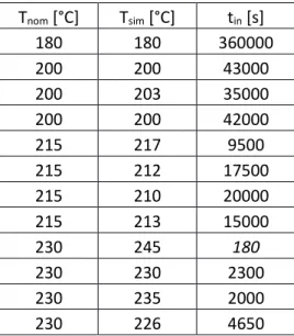
temperatures (180, 200, 215, and 230°C) and these values are reported in Tab. 2. As expected, the
21 Tnom [°C] Tsim [°C] tin [s] 180 180 360000 200 200 43000 200 203 35000 200 200 42000 215 217 9500 215 212 17500 215 210 20000 215 213 15000 230 245 180 230 230 2300 230 235 2000 230 226 4650
Table 2: Incubation time (tinc) obtained from the in situ XRD measurements. Tnom is the nominal temperature.
Tsim is the simulated temperature used to fit the lateral growth of NiSi. The errors bars for temperature and
incubation time were estimated from the fit the lateral growth to be respectively ±2°C and ±1% . For Tsim=
245°C, the value of tinc is lower than the time for a XRD scan leading to a large error.
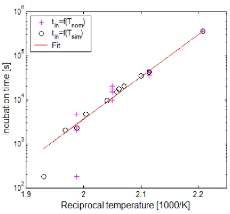
Figure 7 presents the variation of the logarithm of the incubation time as a function of the inverse of
temperature. Two types of temperatures have been used in Fig. 7: either the nominal ones or the ones
used for the simulation of the lateral growth. If the nominal temperature is taken into account, a large
spread of the incubation time is obtained. This spread could correspond to fluctuation in nucleation
that is expected in the classical nucleation theory. However if the incubation times are reported as a
function of the simulated temperature, the spread becomes negligible and a linear relationship is
obtained in the Arrhenius curve as expected from Eq. 9. This is a strongly suggest that the real
temperature are closer to the simulated ones than to the nominal ones. Figure 7 shows thus that the
variation of the logarithm of the incubation time as a function of the inverse of temperature follows a
linear relationship. The activation energy for NiSi nucleation kinetic at the θ-Ni2Si/Si interface
deduced from the fit of these data (Tab. 2) is found to be 1.9 eV and the pre exponential factor tinc0 =3
22 𝑡𝑖𝑛𝑐 = 3 ± 1 10−16𝑒𝑥𝑝 (
1.9 ± 0.05 eV
𝑘𝐵𝑇 ) 𝑠 Eq. 10
Note that a higher activation is obtained (2.2±0.1eV) if the nominal temperature is used instead of the
temperature determined in the lateral growth simulation.
Figure 7: Incubation time as a function of the inverse of temperature. Either the temperature determined in the simulation of the lateral growth (black circles) or the nominal temperature (pink crosses) has been used. The line
corresponds to the exponential fit. The value of 180s for the first annealing at 230°C (Tab. 2) was not taken into account for the fit because of its large uncertainty.
It is worth mentioning that during the incubation time, atoms fluctuation occurs until the formation of
a nucleus with a size larger than a certain threshold. This atoms fluctuation is greatly affected by
temperature changes and a small change in temperature may induce an important variation in the
23 due to the slight variation of temperature during the experiments that were revealed by the change in
lateral growth kinetics (Fig. 4). Even a change of a few percent in the temperature can induce a large
change in the incubation time (Fig. 4 and Tab. 2). This variation of the incubation time is easier to
observe at low temperature since the incubation time is larger: for example, a change of 7°C (from 210
to 217°C) can more than double the incubation time (Tab. 2 and Fig. 7). Our results show that a little
variation in temperature impacts more drastically the reaction kinetics when it is controlled by
nucleation than when it is controlled by diffusion (Fig. 4). This may be of great importance for the
contacts in microelectronics since difference in temperatures may arise due to non-uniformity along
the Si wafer during the heat treatments used to form the contacts. Furthermore, in transistors, Si is
doped with different dopants and doping levels depending on the regions (source, drain, gate). These
dopants can change the formation of NiSi and may have also an impact on the nucleation of NiSi
[7,49]. Similarly the addition of Ge or C used to modify the carrier mobility of the Si semiconductor
may affect the nucleation. As nucleation is expected to occur at defects such as triple line or junction
between triple line and Si interface, it could also depend on the local microstructure (grain size, texture…).
However one should emphasize that our measurements were done at low temperature compared to the
heat treatments performed to fabricate the contacts through the microelectronics processes. Indeed
rapid thermal annealing (RTA) or nanosecond laser annealing (NLA), i.e. heat treatments at high
temperatures for (very) short times, are usually performed in microelectronics. Our low temperature
measurements allow to reveal and measure the incubation times that are relatively large at low
temperature due to the exponential variation but should be much lower at high temperatures. For
example, the incubation will be less than one second accordingly with Eq. 10 at 350°C. For RTA or
NLA, the incubation time may thus not be detected and could have a lower or negligible impact.
At high temperature heat treatment such as RTA or NLA, the mechanisms associated to nucleation
24 the θ-Ni2Si phase is metastable at temperature below 825°C in the Ni-Si system, the driving force
should be lower (and thus not in favor of the NiSi nucleation) but other factors such as the presence of
Pt or the metal to Si concentration ratio could have a reverse effect on the driving force. Nucleation may also change from heterogeneous (i.e. on defects at the θ-Ni2Si/Si interface) to homogeneous (i.e.
at any place of the θ-Ni2Si/Si interface) since, at high temperature, larger fluctuations may allow the
higher energy configurations needed for homogeneous nucleation.
The equation developed for the nucleation incubation time (Eq. 9) is based on the classical nucleation
theory for homogeneous nucleation and is only a crude estimation for the present case where nucleation
occurs on defects at an interface between a silicide et Si. Nevertheless, the exponential law with an
activation energy of 1.9 eV (Eq. 10) is a good fit to the incubation times determined experimentally.
This law should thus allow a better control of the contact formation in microelectronics.
In the classical nucleation theory, the incubation time is required for large enough fluctuation to
overcome the nucleation barrier around nucleation site and thus to obtain nuclei with a size larger than
the critical size. However the time delay for NiSi nucleation may come from some other relaxation
process that could be mechanical and/or diffusive. The possible relaxation processes will be now
examined.
As discussed before, the relaxation of stress was already found to play an important role in the time
delay between the end of the growth of δ-Ni2Si and the formation of NiSi [15]. Arrhenius behaviors
with activation energy around 1.2 and 1.7 eV were found for the time delay in case of pure Ni and Ni(5
at.% Pt) respectively [15]. The time delay was clearly related to the strain relaxation in δ-Ni2Si since
the formation of NiSi occurs only when the strain in δ-Ni2Si is relaxed [15]. However the stress/strain
behavior is complex during the silicide growth [41] [42] and no clear explanation was found for the
link between strain relaxation and the formation of NiSi. Indeed if stress in the nucleating (or growing)
phase (NiSi) may explain difficulty of nucleation (or growth), it is much more difficult to understand
25 time delay between θ-Ni2Si and NiSi (Ea=1.9 eV) is not far the one found for Ni(5 at.% Pt) (Ea=1.7
eV): this might suggest a similar behavior: i.e. the time delay between θ-Ni2Si and NiSi might thus be
related to the stress relaxation in θ-Ni2Si. However, θ-Ni2Si phase is not easily detectable with XRD
and it is thus difficult to measure its stress relaxation. Further investigations with more complex XRD
techniques such as pole figure or 3 dimensional mapping of the reciprocal space may clarify this point.
The stress relaxation in silicides is usually attributed to a creep mechanism that is related to the
diffusion of the less mobile species, Si in the Ni silicide. The increase in activation energy between
pure Ni and Ni(5 at.% Pt) might come from the role of Pt on the diffusion of Si or even to the need of
the diffusion of Pt during creep. The larger activation energy found in our study (Ea=1.9 eV) might
thus be a consequence of the higher content of Pt (10 at.%).
Another explanation for the time delay might be linked to the effect of Pt on the interfacial energy
change. The nucleation of NiSi would be easier if the effect of Pt is to decrease the change in interface
energy (Eq. 6) and thus either increase the energy of the θ-Ni2Si/Si interface or decrease the energy of
the NiSi/Si or θ-Ni2Si/NiSi interface. The redistribution of Pt has been studied in details in [8]: during
the growth of θ-Ni2Si, Pt is incorporated in θ-Ni2Si due to its large solubility but diffuses much less
than Ni in θ-Ni2Si [8]. As a result, at the end of the θ-Ni2Si growth, the Pt concentration is high close
to the surface and decreases almost exponentially with depth in θ-Ni2Si [8]. During the time delay, Pt
should thus diffuse from the θ-Ni2Si surface to the θ-Ni2Si/Si interface to reduce its own concentration
gradient. One may thus expect an increasing content of Pt at the interface between θ-Ni2Si and Si
during the time delay. The Pt profile in θ-Ni2Si when NiSi nucleates, i.e. after the time delay, (Fig.
3.d) is in agreement with the redistribution observed previously [8]. However the concentration of Pt
at the θ-Ni2Si/Si interface is still very low: about 0.1% as shown in Fig 3.d). This could be due to a
limited diffusion of Pt but it is possible that locally (especially at the intersection between the
θ-Ni2Si/Si interface and the θ-Ni2Si grain boundary or triple junction) the Pt concentration is higher.
26 segregation of Pt at the interfaces was observed (Fig. 3) that could change the energies of these
interfaces. Secondly, for the epitaxial relationship between θ-Ni2Si and Si, i.e. (1 1 -2 0) θ-Ni2Si //
(220) Si, the misfit is slightly negative and varies from -0.9 to -0.1% depending on the composition of θ-Ni2Si in the case of pure Ni. As Pt is expected to increase the lattice parameter of θ-Ni2Si because
of its larger size that Ni, a higher Pt content should decrease the misfit and thus give a better epitaxy.
It would thus result in a decrease of the θ-Ni2Si/Si interface energy and thus an increase of the
nucleation barrier rather than the expected decrease. Moreover to induce a change in the misfit the
concentration of Pt at the θ-Ni2Si/Si interface should be more consequent than the 0.1% found in Fig
3.d. Note that it can be locally the case as already mentioned. The redistribution of Pt may thus not be
directly at the origin of the time delay. It has also been shown that the presence of Pt change the texture
of the Ni silicide [50] that is a complex combination of epitaxy, axiotaxy, as well as fiber and random
components [35]. However it is not clear how the redistribution of Pt can change the texture and how
this can be related to the time delay.
Another relaxation mechanism could be related to the non-stoichiometry of the θ-Ni2Si phase. Indeed
for nucleation to occur, the composition of the nucleating phase has to be reached locally [11]. The
incubation time may be related to the time needed for the local composition to reach the one of NiSi.
This time could be related to diffusion of Ni, Pt and/or Si in θ-Ni2Si and their dependency of
composition of the θ-Ni2Si.
All these mechanisms and their combination could be at the origin of the time delay but it is difficult
at this stage to attribute the observed time delay to one (or several) of these mechanisms or to a classical
(heterogeneous or homogenous) nucleation mechanism. More experiments with advanced
characterization in order to better characterize these time delay should give a better understanding. A
specific point might be to determine the fluctuation of nucleation events within a given sample in
comparison to the one between several samples prepared in the same way. Another important point
27 lines… More fundamentally it is important to understand the nucleation at an interface between different materials. Whatsoever our results provide insights on these topics by determining how the
incubation time varies with temperature. The obtained activation energy (1.9 eV) is in agreement with
the well-known semi-empirical rule saying that nucleation is suppressed for nucleation barrier higher
than about 60-70 kBT and has reasonable rate for nucleation barrier of about 30 kBT. Indeed, it
correspond to a value of about 40 kT. Alternatively, the value of the activation energy could correspond
to the relaxation mechanism detailed above. The determination of the physical meaning of tinc0 and Ea
will require more investigations especially in term of simulation and modeling.
5. Conclusion
To conclude, several in situ XRD isothermal annealing were performed on the 10 nm Ni (10 at.% Pt)/
Si (100) in order to investigate the formation of NiSi at the epitaxial θ-Ni2Si/Si interface. These results
show an incubation time before the beginning of NiSi formation which varies with temperature. These
variations appeared to be related to nucleation difficulty of the NiSi phase at the epitaxial θ-Ni2Si/Si
interface with a low energy. The activation energy for NiSi nucleation at the expense of θ-Ni2Si was
estimated 1.9 eV by plotting the variation of the incubation time as a function of the inverse of the
temperature. The NiSi growth determined by in-situ XRD were fitted with the Coffey’s model which
allows the deduction of lateral growth kinetics (ELG=1.75 eV). This fitting suggests that after
nucleation of the NiSi phase, lateral growth has a major contribution to the phase formation.
Acknowledgments
This work was supported by the CNRS-CEA “METSA” French network (FR CNRS 3507) for the
28 T. Epicier is greatly acknowledged for TEM measurements and M. Descoins and M. Bertoglio for
technical assistance.
References
[1] R.W. Mann, L.A. Clevenger, P.D. Agnello, F.R. White, Silicides and local interconnections for high-performance VLSI applications, IBM J. Res. Dev. 39 (1995) 403–417.
https://doi.org/10.1147/rd.394.0403.
[2] K.N. Tu, W.K. Chu, J.W. Mayer, Structure and growth kinetics of Ni2Si on silicon, Thin Solid Films. 25 (1975) 403–413. https://doi.org/10.1016/0040-6090(75)90058-9.
[3] C. Detavernier, A. Özcan, C. Lavoie, J.-J. Sweet, J.M.E. Harper, Kinetics of agglomeration of NiSi and NiSi2 phase formation., MRS Online Proc. Libr. Arch. 745 (2002).
https://doi.org/10.1557/PROC-745-N4.12.
[4] D. Mangelinck, J.Y. Dai, J.S. Pan, S.K. Lahiri, Enhancement of thermal stability of NiSi films on (100)Si and (111)Si by Pt addition, Appl. Phys. Lett. 75 (1999) 1736–1738.
https://doi.org/10.1063/1.124803.
[5] C. Lavoie, F.M. d’Heurle, C. Detavernier, C. Cabral Jr., Towards implementation of a nickel silicide process for CMOS technologies, Microelectron. Eng. 70 (2003) 144–157.
https://doi.org/10.1016/S0167-9317(03)00380-0.
[6] F. Panciera, K. Hoummada, M. Gregoire, M. Juhel, N. Bicais, D. Mangelinck, Three dimensional distributions of arsenic and platinum within NiSi contact and gate of an n-type transistor, Appl. Phys. Lett. 99 (2011) 051911. https://doi.org/10.1063/1.3616150.
[7] F. Panciera, La sonde atomique tomographique : applications aux dispositifs CMOS avancés sub-45nm, (2012).
[8] F. Panciera, K. Hoummada, M. Gregoire, M. Juhel, D. Mangelinck, Pt redistribution in N-MOS transistors during Ni salicide process, Microelectron. Eng. 107 (2013) 173–177.
https://doi.org/10.1016/j.mee.2013.01.029.
[9] M. Putero, L. Ehouarne, E. Ziegler, D. Mangelinck, First silicide formed by reaction of
Ni(13%Pt) films with Si(1 0 0): Nature and kinetics by in-situ X-ray reflectivity and diffraction, Scr. Mater. 63 (2010) 24–27. https://doi.org/10.1016/j.scriptamat.2010.02.040.
[10] F. Panciera, D. Mangelinck, K. Hoummada, M. Texier, M. Bertoglio, A. De Luca, M. Gregoire, M. Juhel, Direct epitaxial growth of θ-Ni2Si by reaction of a thin Ni(10 at.% Pt) film with Si(1 0 0) substrate, Scr. Mater. 78–79 (2014) 9–12. https://doi.org/10.1016/j.scriptamat.2014.01.010. [11] M. El Kousseifi, K. Hoummada, M. Bertoglio, D. Mangelinck, Selection of the first Ni silicide
phase by controlling the Pt incorporation in the intermixed layer, Acta Mater. 106 (2016) 193– 198. https://doi.org/10.1016/j.actamat.2016.01.004.
29 [12] F. d’Heurle, C.S. Petersson, J.E.E. Baglin, S.J. La Placa, C.Y. Wong, Formation of thin films of
NiSi: Metastable structure, diffusion mechanisms in intermetallic compounds, J. Appl. Phys. 55 (1984) 4208. https://doi.org/10.1063/1.333021.
[13] F.M. d’Heurle, Nucleation of a new phase from the interaction of two adjacent phases: Some silicides, J. Mater. Res. 3 (1988) 167–195. https://doi.org/10.1557/JMR.1988.0167.
[14] A. Alberti, C. Spinella, A. La Magna, E. Rimini, Nucleation and growth of NiSi from Ni2Si transrotational domains, Appl. Phys. Lett. 90 (2007) 053507.
https://doi.org/10.1063/1.2437058.
[15] D. Mangelinck, K. Hoummada, Effect of stress on the transformation of Ni2Si into NiSi, Appl. Phys. Lett. 92 (2008) 254101. https://doi.org/10.1063/1.2949751.
[16] M. El Kousseifi, K. Hoummada, T. Epicier, D. Mangelinck, Direct observation of NiSi lateral growth at the epitaxial θ-Ni2Si/Si(1 0 0) interface, Acta Mater. 99 (2015) 1–6.
https://doi.org/10.1016/j.actamat.2015.07.062.
[17] D. Mangelinck, M. El Kousseifi, K. Hoummada, F. Panciera, T. Epicier, Lateral growth of NiSi at the θ-Ni2Si/Si(100) interface: Experiments and modelling, Microelectron. Eng. 199 (2018) 45–51. https://doi.org/10.1016/j.mee.2018.07.014.
[18] B. Gault, M.P. Moody, F.D. Geuser, A.L. Fontaine, L.T. Stephenson, D. Haley, S.P. Ringer, Spatial Resolution in Atom Probe Tomography, Microsc. Microanal. 16 (2010) 99–110. https://doi.org/10.1017/S1431927609991267.
[19] T.F. Kelly, D.J. Larson, The second revolution in atom probe tomography, Mrs Bull. 37 (2012) 150–158. https://doi.org/10.1557/mrs.2012.3.
[20] K. Coffey, L. Clevenger, K. Barmak, D. Rudman, C. Thompson, Experimental-Evidence for Nucleation During Thin-Film Reactions, Appl. Phys. Lett. 55 (1989) 852–854.
https://doi.org/10.1063/1.102447.
[21] K. Coffey, K. Barmak, D. Rudman, S. Foner, Thin-Film Reaction-Kinetics of Niobium
Aluminum Multilayers, J. Appl. Phys. 72 (1992) 1341–1349. https://doi.org/10.1063/1.351744. [22] C. Bergman, E. Emeric, G. Clugnet, P. Gas, Kinetics of Reactive Diffusion in Al/Co
Multilayers, Defect Diffus. Forum. 194–199 (2001) 1533–1538. https://doi.org/10.4028/www.scientific.net/DDF.194-199.1533.
[23] F. Nemouchi, D. Mangelinck, C. Bergman, P. Gas, U. Smith, Differential scanning calorimetry analysis of the linear parabolic growth of nanometric Ni silicide thin films on a Si substrate, Appl. Phys. Lett. 86 (2005) 041903. https://doi.org/10.1063/1.1852727.
[24] K. Hoummada, D. Mangelinck, A. Portavoce, Kinetic of Formation of Ni and Pd Silicides: Determination of Interfacial Mobility and Interdiffusion Coefficient by In Situ Techniques, Solid State Phenom. 172–174 (2011) 640–645.
https://doi.org/10.4028/www.scientific.net/SSP.172-174.640.
[25] K. Hoummada, A. Portavoce, C. Perrin-Pellegrino, D. Mangelinck, C. Bergman, Differential scanning calorimetry measurements of kinetic factors involved in salicide process, Appl. Phys. Lett. 92 (2008) 133109. https://doi.org/10.1063/1.2905293.
[26] G. Lucadamo, K. Barmak, S. Hyun, C. Cabral Jr., C. Lavoie, Evidence of a two-stage reaction mechanism in sputter deposited Nb/Al multilayer thin-films studied by in situ synchrotron X-ray diffraction, Mater. Lett. 39 (1999) 268–273. https://doi.org/10.1016/S0167-577X(99)00017-8.
[27] R. Delattre, O. Thomas, C. Perrin-Pellegrino, C. Rivero, R. Simola, First stage of CoSi2 formation during a solid-state reaction, J. Appl. Phys. 116 (2014) 245301.
https://doi.org/10.1063/1.4904852.
[28] B.E. Deal, A.S. Grove, General Relationship for the Thermal Oxidation of Silicon, J. Appl. Phys. 36 (1965) 3770. https://doi.org/10.1063/1.1713945.
[29] L.A. Clevenger, C.V. Thompson, R.C. Cammarata, K.N. Tu, Reaction kinetics of nickel/silicon multilayer films, Appl. Phys. Lett. 52 (1988) 795–797. https://doi.org/10.1063/1.99644.
30 [30] J. Demeulemeester, D. Smeets, C.M. Comrie, N.P. Barradas, A. Vieira, C. Van Bockstael, C.
Detavernier, K. Temst, A. Vantomme, On the growth kinetics of Ni(Pt) silicide thin films, J. Appl. Phys. 113 (2013) 163504. https://doi.org/10.1063/1.4802738.
[31] K. Hoummada, Etude de la redistribution des dopants et des éléments d’alliages lors de la formation des siliciures, Université Paul Cézanne, 2007.
[32] M. El Kousseifi, Ni silicide contacts: Diffusion and reaction in nanometric films and nanowires, Aix-Marseille University, 2014.
[33] A. Yelon, B. Movaghar, Microscopic explanation of the compensation (Meyer-Neldel) rule, Phys. Rev. Lett. 65 (1990) 618–620. https://doi.org/10.1103/PhysRevLett.65.618.
[34] J. Philibert, Some thoughts and/or questions about activation energy and pre-exponential factor, in: B.S. Bokstein, B.B. Straumal (Eds.), Diffus. Solids - Past Present Future, 2006: pp. 61–72. [35] B. De Schutter, K. De Keyser, C. Lavoie, C. Detavernier, Texture in thin film silicides and
germanides: A review, Appl. Phys. Rev. 3 (2016) 031302. https://doi.org/10.1063/1.4960122. [36] D. Mangelinck, T. Luo, C. Girardeaux, Reactive diffusion in the presence of a diffusion barrier:
Experiment and model, J. Appl. Phys. 123 (2018) 185301. https://doi.org/10.1063/1.5023578. [37] L. Klinger, Y. Bréchet, G. Purdy, On the kinetics of interface-diffusion-controlled peritectoid
reactions, Acta Mater. 46 (1998) 2617–2621. https://doi.org/10.1016/S1359-6454(97)00471-0. [38] M. Pasichnyy, A. Gusak, Model of Lateral Growth Stage during Reactive Phase Formation,
Defect Diffus. Forum. 277 (2008) 47–52.
https://doi.org/10.4028/www.scientific.net/DDF.277.47.
[39] V. Vovk, G. Schmitz, R. Kirchheim, Nucleation of product phase in reactive diffusion of Al/Co, Phys. Rev. B. 69 (2004) 104102. https://doi.org/10.1103/PhysRevB.69.104102. [40] G. Lucenko, A. Gusak, A model of the growth of intermediate phase islands in multilayers,
Microelectron. Eng. 70 (2003) 529–532. https://doi.org/10.1016/S0167-9317(03)00432-5. [41] F.M. d’Heurle, O. Thomas, Stresses during Silicide Formation: A Review, Defect Diffus.
Forum. 129–130 (1996) 137–150. https://doi.org/10.4028/www.scientific.net/DDF.129-130.137.
[42] S.-L. Zhang, F.M. d’Heurle, Stresses from solid state reactions: a simple model, silicides, Thin Solid Films. 213 (1992) 34–39. https://doi.org/10.1016/0040-6090(92)90471-M.
[43] T.G. Finstad, A Xe marker study of the transformation of Ni2Si to NiSi in thin films, Phys. Status Solidi A. 63 (1981) 223–228. https://doi.org/10.1002/pssa.2210630130.
[44] D. Mangelinck, K. Hoummada, I. Blum, Kinetics of a transient silicide during the reaction of Ni thin film with (100)Si, Appl. Phys. Lett. 95 (2009) 181902.
https://doi.org/10.1063/1.3257732.
[45] M. El Kousseifi, K. Hoummada, D. Mangelinck, Ni silicide study at the atomic scale: Diffusing species, relaxation and grooving mechanisms, Acta Mater. 83 (2015) 488–498.
https://doi.org/10.1016/j.actamat.2014.10.029.
[46] D. Mangelinck, K. Hoummada, A. Portavoce, C. Perrin, R. Daineche, M. Descoins, D.J.
Larson, P.H. Clifton, Three-dimensional composition mapping of NiSi phase distribution and Pt diffusion via grain boundaries in Ni2Si, Scr. Mater. 62 (2010) 568–571.
https://doi.org/10.1016/j.scriptamat.2009.12.044.
[47] E. Clouet, Modeling of Nucleation Processes, in: ASM Handb. Vol. 22A Fundam. Model. Met. Process., D. U. Furrer and S. L. Semiatin, 2009: pp. 203–219.
[48] K.F. Kelton, A.L. Greer, C.V. Thompson, Transient nucleation in condensed systems, J. Chem. Phys. 79 (1983) 6261–6276. https://doi.org/10.1063/1.445731.
[49] D. Mangelinck, K. Hoummada, F. Panciera, M. El Kousseifi, I. Blum, M. Descoins, M. Bertoglio, A. Portavoce, C. Perrin, M. Putero, Progress in the understanding of Ni silicide formation for advanced MOS structures, Phys. Status Solidi -Appl. Mater. Sci. 211 (2014) 152– 165. https://doi.org/10.1002/pssa.201300167.
31 [50] C. Detavernier, C. Lavoie, Influence of Pt addition on the texture of NiSi on Si(001), Appl.


![Table 1: Values of the parameters for the lateral growth obtained in this study compared to the values obtained in literature for Pd 2 Si, Ni 2 Si and NbAl 3 [20,24]](https://thumb-eu.123doks.com/thumbv2/123doknet/14641217.735318/15.892.114.786.518.738/table-values-parameters-lateral-obtained-compared-obtained-literature.webp)
![Figure 5: Arrhenius representation of the kinetics parameters for the lateral growth a) Velocity for silicide b) Product of nucleation site density by the lateral growth velocity for NiSi compared the other intermetallic compounds [20,24]](https://thumb-eu.123doks.com/thumbv2/123doknet/14641217.735318/16.892.144.753.422.695/arrhenius-representation-kinetics-parameters-velocity-nucleation-intermetallic-compounds.webp)