HAL Id: hal-02263526
https://hal-amu.archives-ouvertes.fr/hal-02263526
Submitted on 10 Nov 2020HAL is a multi-disciplinary open access archive for the deposit and dissemination of sci-entific research documents, whether they are pub-lished or not. The documents may come from teaching and research institutions in France or abroad, or from public or private research centers.
L’archive ouverte pluridisciplinaire HAL, est destinée au dépôt et à la diffusion de documents scientifiques de niveau recherche, publiés ou non, émanant des établissements d’enseignement et de recherche français ou étrangers, des laboratoires publics ou privés.
Terrestrial Neutron-Induced Single Events in GaN
Daniela Munteanu, Jean-Luc Autran
To cite this version:
Daniela Munteanu, Jean-Luc Autran. Terrestrial Neutron-Induced Single Events in GaN. Micro-electronics Reliability, Elsevier, 2019, 100-101, pp.113357. �10.1016/j.microrel.2019.06.049�. �hal-02263526�
1
Terrestrial Neutron-Induced Single Events in GaN
D. Munteanu
a, J.L. Autran
a,*
a Aix-Marseille University & CNRS, IM2NP (UMR 7334), Faculté des Sciences – Service 142,
Avenue Escadrille Normandie Niémen, F-13397 Marseille Cedex 20, France
Abstract
We study the physical mechanisms of single event production in GaN wide-bandgap semiconductor subjected to atmospheric high-energy (> 1 MeV) neutron irradiation. The interactions of incident neutrons with the target material are investigated with Geant4 and the transport of the deposited charge simulated using our random-walk drift-diffusion (RWDD) modelling approach in a generic reversely biased bulk junction.
Keywords
Gallium nitride, single events, atmospheric neutrons, neutron interactions, Geant4, radiation transport, random-walk drift-diffusion
Highlights
• Interactions of atmospheric neutrons with GaN materials are investigated using Geant4 simulations • Secondaries produced in GaN are characterized in terms of energy, linear energy transfer and range • Single event transients induced by alpha particles in GaN bulk junction are simulated
• Implications for the occurrence of single events in GaN material with respect to Si are discussed
* Corresponding author:
Prof. Jean-Luc Autran, IM2NP - UMR CNRS 7334, Faculté des Sciences – Service 142, Avenue Escadrille Normandie – F-13397 Marseille Cedex 20 France – Phone: + 33 (0)413 594 627 – Email: [email protected]
2
1. Introduction
There is a growing interest in gallium nitride (GaN) for applications in optoelectronic, power, high-temperature and high-frequency devices, due to its exceptional properties (with respect to silicon in particular) in terms of very high breakdown voltages, high electron mobility and saturation velocity. GaN is also a very hard mechanically stable wide bandgap semiconductor material, known to its robustness and stability in radiation environments; its interest for nuclear particle detection is essential [1-4]. More recent growing application-markets (electrical cars, space and avionics) for which high reliability power electronics is needed has accentuated the importance of GaN-based microelectronics and technologies [4-5].
For terrestrial applications, the radiation response of GaN subjected to atmospheric neutrons has been little studied so far [6]. The aim of this work is precisely to investigate the physical mechanisms of single event production in GaN induced by high-energy (>1 MeV) neutrons in the atmosphere.
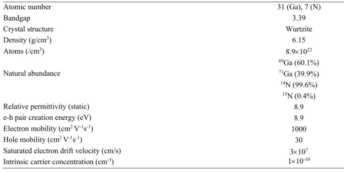
Atomic number 31 (Ga), 7 (N)
Bandgap 3.39
Crystal structure Density (g/cm3)
Atoms (/cm3)
Natural abundance
Relative permittivity (static) e-h pair creation energy (eV) Electron mobility (cm2 V-1s-1)
Hole mobility (cm2 V-1s-1)
Saturated electron drift velocity (cm/s) Intrinsic carrier concentration (cm-3)
Wurtzite 6.15 8.9´1022 69Ga (60.1%) 71Ga (39.9%) 14N (99.6%) 15N (0.4%) 8.9 8.9 1000 30 3´107 1´10-10
Table 1. Main properties of GaN (300 K).
Table 1 summarizes the main properties of bulk GaN considered in this work. With respect to silicon, GaN exhibits a larger bandgap, density and e-h pair creation energy. In addition and due to a difference in the nature of the target atoms (higher Z for Ga), these changes in physical key-parameters suggest that the neutron irradiation behavior of GaN with respect to silicon should be different, as shown in the following sections of the paper. Section 2 presents the detailed analysis of atmospheric neutron-GaN interactions; section 3 investigates ion transport and energy
3
transfer in GaN. Finally, section 4 explores the charge transport and diffusion-collection mechanism in a reversely biased bulk junction representative of the studied technology. These three steps cover all the physical mechanisms responsible of single-event production in bulk GaN from nuclear interactions up to the creation of the resulting transient current pulse at the level of a reversely-biased collector contact at device level.
2. Interactions of atmospheric neutrons with GaN 2.1. Simulation details
A volume of 1cm2´20µm-thick of stoichiometric GaN material was irradiated in normal incidence with 108
atmospheric neutrons (equivalent to 570 years at sea-level) in Geant4 simulations [7-8], considering the differential flux spectrum of neutrons (E> 1 MeV) measured by Gordon, Goldhagen et al. in Yorktown Heights [9] as the input distribution for the Geant4 general particle source [10]. The list of physical processes employed in simulation (Geant4 version 4.9.4 patch 01 [11]) is based on the standard package of physics lists QGSP_BIC_HP, as described in [5,12]. Output simulation results consist of a series of records describing all the neutron interaction events in the target material, including for each event the nature and the vertex coordinates of the interaction, the energy of the incident neutron, the resulting secondary products, their energies and emission direction vectors. A database post-treatment eliminates in the database all secondary particles not able to induce a single event, i.e. not able to deposit an electrical charge in the target material above a certain threshold quantity, fixed in previous studies at 1.8 fC [5,13,14]. Such eliminated particles include the less energetic recoils, all neutrons not interacting with the target and all g photons, p0, rare p+ and p-, e+, e- and h particles. Note that the interaction events caused by
secondary neutrons (in cascade) are considered in the database.
2.2. Simulation results
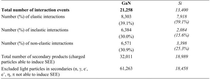
The atmospheric neutron-GaN interaction database resulting from the interaction of 108 neutrons with a 1cm2
´ 20µm-thick GaN target contains 21,258 events, as detailed in Table 2. For comparison, the same information for a target in Si is indicated.
4
GaN Si
Total number of interaction events 21,258 13,400
Number (%) of elastic interactions 8,303 (39.1%)
7,918 (59.1%)
Number (%) of inelastic interactions 6,384 (30.0%)
2,084 (15.6%)
Number (%) of non-elastic interactions 6,571 (30.9%)
3,398 (25.3%)
Total number of secondary products (charged
particles able to induce SEE) 32,011 18,989 Excluded light particles in secondaries (n, g, e-,
e+, h, p not able to induce SEE)
61,263 18,458
Table 2. Main properties of the computed atmospheric neutrons-GaN interaction database. The same metrics for bulk Si are also indicated for comparison (partially from [6]).
Interactions of neutrons with atomic nuclei can be divided in two major mechanisms [15-16]: scattering (elastic, inelastic) and capture (or non-elastic). In the elastic scattering, the nature of the interacting particles is not modified; the recoil nucleus is then the same as the target nucleus (Ga or N in the present case). The inelastic scattering is similar to the elastic scattering except that the target nucleus undergoes an internal rearrangement into an excited state from which it eventually releases radiation. Instead of being scattered, an incident neutron may be absorbed or captured by a target material nucleus. Many reactions are possible and a large variety of particles can be emitted. This type of interaction is also called non-elastic interaction. Table 2 gives the number and percentages of elastic, inelastic and non-elastic interaction events; it also indicates the total number of secondaries (32,011 charged particles) considered in the following (i.e. able to induce SEE) and the number of light particles excluded (61,263 for GaN including 37,116 gamma photons and 23,938 secondary neutrons; 18,409 for Si, 11,451 gammas, 6,811 secondary neutrons). In the end, elastic + inelastic interactions represent for GaN 69.1 % of the total of the events present in the database (resp. 74.7% for Si); each interaction of these types produces a single Ga or N (resp. Si) recoil nucleus in the target. For GaN, a large majority (84%) of elastic interactions involve N nuclei (low-Z element), the remaining 16% are due to elastic scattering with Ga nuclei. On the contrary, inelastic scatterings are essentially due to interactions with Ga nuclei (93%), the remaining 7% being due to N. Concerning now non-elastic interactions, they represent 30.9% of the events for GaN (against 25.3% for Si); they produce two or more particles ranging from protons to C for n-N interactions and from proton to Zn for n-Ga events.
5
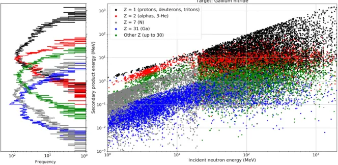
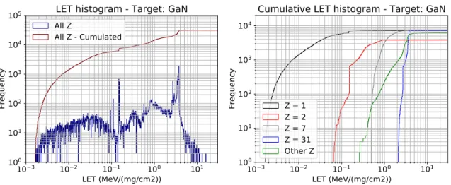
function of the incident neutron energy (right) for all secondaries produced in the 21,258 events recorded in the n-GaN database. Similarly, Fig. 2 shows the same graphics for the n-Si database. For n-GaN, five groups of secondaries have been defined as a function of their atomic number: Z=1 (7297 particles for GaN with 80% of protons, 15% of deuterons and 5% of tritons), Z=2 (3781 particles, 96% a, 4% 3He), Z=7 and Z=31 (N and Ga recoil nuclei,
respectively) and other Z (ranging from 3 to 30, excluding 7). Figure 1 (right) shows that, contrary to silicon (Fig. 2 right), low energy atmospheric neutrons (from 1 to 10 MeV) induce in GaN a significant amount of low energy (E£10 MeV) protons, alpha and other ions (B and C especially) produced in 14N(n,p)14C and 14N(n,a)11B reactions.
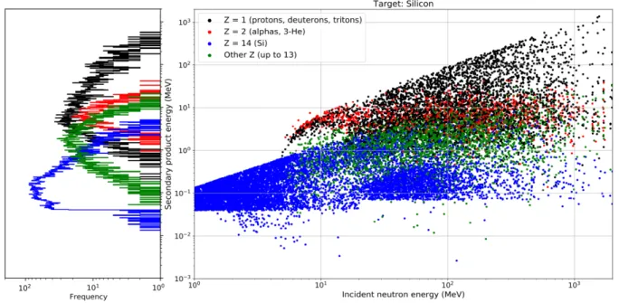
Compared with the silicon map, this excess of low energy products for GaN is well visible in the rectangular energy domain delimited by the values 1 and 10 MeV on the two axis. For silicon, four groups of products are defined for comparison: Z = 1 (4462 particles, 89% alpha, 9% deuteron and 2% triton), Z = 2 (1131 particles, 95% alpha, 5% 3He), Z = 14 (Si) and other Z ranging from 3 to 13. Energy histograms for these product groups are
shown in Fig. 1 (left) for GaN and in Fig. 2 (left) for Si. These distributions evidence the larger numbers of products for all the groups related to GaN with respect to Si, notably for Z = 1 (mainly protons) and Z = 2 (mainly alphas).
Fig. 1. Energy histogram as a function of the secondary product energy (left) and energy distribution as a function
of the incident neutron energy (right) for all secondaries produced in the 21,258 events recorded in the n-GaN database.
6
Fig. 2. Energy histogram as a function of the secondary product energy (left) and energy distribution as a function
of the incident neutron energy (right) for all secondaries produced in the 13,400 events recorded in the n-Si database.
3. Ion transport in GaN and creation of e-h pairs
The SRIM (the Stopping and Range of Ions in Matter) [17] was used in this work to determine the initial LET and range in GaN of all secondary charged products of the database. A behavioral modeling of SRIM data [18] was also used to compute the profile of the electrical charge deposited along their tracks for results shown in Section 4, considering an average value of 8.9 eV for the creation of an e-h pair in bulk GaN.
Figures 3 and 4 show the energy distributions of the LET values for all the secondaries contained in the n-GaN and n-Si databases. From left histograms of Figs. 3 and 4, we can deduce that high LET particles above 1 MeV cm2 mg-1 are globally more numerous for GaN than for Si (+33%), as well for low LET values below 10-1
MeV cm2 mg-1 (+50%). Between 10-1 and 1 MeV/(mg/cm2), this increase is the most important, with a factor equal
to ´4 for GaN with respect to Si. The cumulative histograms of Figs. 3 and 4 (right) show similar minimum LETs for the distributions of particles with Z = 1 (mainly protons) and for Ga and Si recoils. For Z = 2 and for other Z, this minimum LET is clearly below for GaN with respect to Si.
7
Fig. 3. LET histogram (left) and cumulated LET histogram for secondaries produced in GaN.
Fig. 4. LET histogram (left) and cumulated LET histogram for secondaries produced in Si.
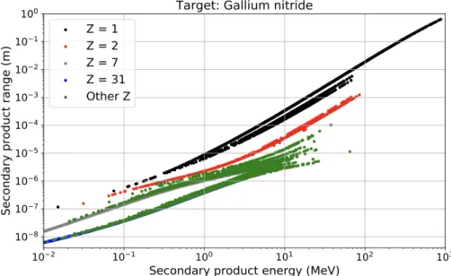
Figure 5 shows the range distributions of all secondaries produced in GaN. For Z = 1, three distinct branches for proton, deuteron and triton are well visible; also the two branches for Z = 2 (alpha particles and 3He) and for
some isotopes of different ions (other Z). Due to the higher density of GaN bulk material with respect to Si (factor ´2.6), particle ranges are shorter in GaN than in Si by a factor ~2. A 5 MeV alpha particle will have a range of 25 µm in Si and only 12 µm in GaN, as illustrated by the particle energy loss profiles shown in Fig. 6.
8
Fig. 5. Range distributions of all secondaries of the database produced in GaN.
Fig. 6. Energy loss of an alpha particle of 5 MeV in Si and in GaN.
4. Single-Event Transient (SET) production in a reversely-biased junction 4.1. Simulation approach
In this last section, we use the random-drift diffusion (RWDD) approach to compute single-event transients [19] in an abrupt p-n junction in order to briefly examine and compare the magnitudes of single event transient currents in bulk GaN with the ones obtained in a similar Si structure with the same ions.
For memory, the RWDD model [20-21] is based on a simplified transport equation reduced to 3D spherical charge carrier diffusion and electric field induced drift. The diffusive process is modeled using a random-walk
9
algorithm [22] whereas the drift-induced motion is directly evaluated from the electrical field developed in the space charge region of the collecting structure. Considering a charge packet initially at the position (x, y, z) at time t, its new position at time t+dt is given by (x+dy, y+dy, z+dz) with:
dx = N1 × (Ddt)1/2 + Ex×µdt
dy = N2 × (Ddt)1/2 + Ey×µdt (1)
dz = N3 × (Ddt)1/2 + Ez×µdt
where N1, N2 and N3 are three independent normal random numbers, D is the diffusion coefficient, µ is the carrier
mobility, and E(Ex, Ey, Ez) is the electric field vector at the corresponding position and time. The transient current
at the collecting node is directly computed from the carrier flux extracted by the contact [20], after eliminating a certain number of carriers during transport due to recombination processes. The “granular” nature of this approach (charge packets) explains the stochastic fluctuations observed on current pulses (see section 4.2).
4.2. Simulation results
We considered an abrupt p-n junction, shown in Fig. 7 (left), with values of acceptor and donor concentrations, respectively NA = 1016 cm-3 and ND = 1019 cm-3 compatible with both Si and GaN technologies [4]. Simulations
have been performed for the same reverse bias condition (VR = 2V), also considering the same minority carrier
lifetime for GaN and Si (10-8 s) [4].
Fig. 7. Schematic representation of the reversely-biased p-n junction in GaN or Si and definition of the two
positions for the passage of the alpha particle in the structure. W is the width of the space charge region.
W( VR ) p-SC (SC = GaN or Si) (NA= 1016cm-3) n+-SC (ND= 1019cm-3) VR i(t) (1) (2) EF EF = 0 DZ DZ 3D diffusion + 1D drift 3D diffusion
10
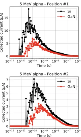
A 5 MeV alpha particle was emitted from two different locations in vertical direction, as schematized in Fig. 7 (with Dz = 0.2 µm in this case). The corresponding single event transients for both GaN and Si materials are shown in Fig. 8. From this example and from other simulation data with other ions and energies (not shown), we can deduce that GaN transients are 2 to 3 times lower in intensity (maximum current). This reduction factor depends on the dominant mechanism (drift – position #1 or diffusion – position #2) controlling the pulse formation and is due to the combined variations of different material or electrical parameters given in Table 3. Then, the large value for e-h pair creation in GaN (8.9 eV) with respect to silicon (3.6 eV) combined with a lower mobility and a higher electric field in the junction leads to a current transient peak reduced by a factor of approximately 2.3 in GaN with respect to Si for the same incident ion and energy. Such synergies between physical mechanisms involved in SET generation should be more deeply investigated in future dedicated studies, also considering other architectures (mostly heterojunctions with 2DEG channel region) more representative of devices of interest for GaN technologies.
Fig. 8. Single event transient currents resulting from the passage of a 5 MeV alpha particle in the positions #1 and #2 for Si and GaN.
11
Evaluated or given quantities Relative variation e-h pair energy creation ÷2.47
Electron mobility ÷1.45
Minority carrier lifetime »1 (by default) Electric field in the space charge region of the junction ´1.56
Table 3. Relative variations of several quantities evaluated for GaN with respect to Si.
5. Conclusion
Our simulation results clearly show that, on one hand, the number of interactions between atmospheric neutrons and GaN is clearly much higher than with Si. All types of interactions events are concerned: elastic scatterings (+5% with respect to Si), inelastic scatterings (+206%) and non-elastic events (+93%). Moreover, the numbers of protons and alpha particles produced in n-GaN interactions are also more important than for n-Si, respectively +45% and +237%. On the other hand, single event pulse formation in a collecting junction shows a reduction in intensity by a factor 2-3 for GaN with respect to Si, due to the combination of several material and electrical parameter with large differences between the two materials, primarily the e-h pair creation energy and carrier mobility. Considering these two main results, our results suggest that the SER due to atmospheric neutrons in GaN devices or circuits would be not necessarily higher (due to the increased number of interactions) or lower (due to the reduction of SET amplitudes) than in Si. However, for certain types of GaN devices, charge collection would preferentially occur in the 2DEG channel region where the mobility is much higher than in a classical bulk p-n junction, and the traps density, piezoelectric fields, interface charges are important factors that may affect the collected current by orders of magnitude. Quantitative studies on given circuit architectures on GaN with should allow us to determine the exact level of the SER in future works to come.
References
[1] Kumar S, Reshi BA, Varma R. Comparison of Silicon, Germanium, Gallium Nitride, and Diamond for using as a detector material in experimental high energy physics. Results in Physics 11 (2018) 461-474. [2] Wang J, Mulligan P, Brillson L, Cao LR. Review of using gallium nitride for ionizing radiation detection.
Applied Physics Reviews 2 (2015) 031102.
12
GaN Devices. ECS Journal of Solid State Science and Technology 5(2) (2016) Q35-Q60.
[4] Zhang Y, Dadgar A, Palacios T. Gallium nitride vertical power devices on foreign substrates: a review and outlook. J. Phys. D: Appl. Phys. 51 (2018) 273001.
[5] De Paula WJ, Tavares PL, De C. Pereira D, Tavares GM, Silva FL et al. A review on gallium nitride switching power devices and applications. IEEE Brazilian Power Electronics Conference, 2017.
[6] Munteanu D and Autran JL. Susceptibility of Group-IV and III-V Semiconductor-based Electronics to Atmospheric Neutrons Explored by Geant4 Numerical Simulations. In: S. Rao (Ed.) Numerical Simulations, Intech, Vienna, 2018, pp. 117-134.
[7] Agostinelli S, et al. Geant4 – a simulation toolkit. Nuclear Instruments and Methods in Physics Research Section A: Accelerators, Spectrometers, Detectors and Associated Equipment 506(3) (2003) 250-303. [8] Allison J, Amako K, Apostolakis J, Arce P, Asai M et al. Recent developments in Geant4. Nuclear
Instruments and Methods in Physics Research Section A: Accelerators, Spectrometers, Detectors and Associated Equipment, 835 (2016) 186-225.
[9] Gordon MS, Goldhagen P, Rodbell KP, Zabel TH, Tang HHK, Clem JM, Bailey P. Measurement of the Flux and Energy Spectrum of Cosmic-Ray Induced Neutrons on the Ground. Transactions on Nuclear Science 51 (2004) 3427-3434.
[10] Geant4 General Particle Source (GPS). Online available: https://geant4.web.cern.ch/ [11] Geant4 version 4.9.4. Online available for download: https://geant4.web.cern.ch.
[12] Autran JL, Serre S, Semikh S, Munteanu D, Gasiot G, Roche P. Soft-Error Rate Induced by Thermal and Low Energy Neutrons in 40 nm SRAMs. IEEE Transactions on Nuclear Science 59 (2012) 2658-2665. [13] Serre S, Semikh S, Uznanski S, Autran JL, Munteanu D, et al. Geant4 analysis of n-Si nuclear reactions
from different sources of neutrons and its implication on soft-error rate. IEEE Transactions on Nuclear Science 59 (4,1) (2012) 714-722
[14] Liu H, Cotter M, Datta S, Narayanan V. Technology Assessment of Si and III-V FinFETs and III-V Tunnel FETs from Soft Error Rate Perspective. International Electron Device Meeting, Institute of Electrical and Electronics Engineers, 2012, pp. 577-580.
[15] Rinard P. Neutron Interactions with Matter. Los Alamos Technical Report (1991).
[16] Autran JL, Munteanu D. Soft Errors: from particles to circuits. Taylor & Francis/CRC Press, 2015, pp. 118-121.
13
[17] Ziegler JF, Ziegler MD, Biersack JP. SRIM – The stopping and range of ions in mater (2010). Nuclear Instruments and Methods in Physics Research Section B: Beam Interactions with Materials and Atoms. 268 (11) (2010) 1818-1823.
[18] Martinie S, Saad-Saoud T, Moindjie S, Munteanu D, Autran JL. Behavioral modeling of SRIM tables for numerical simulation. Nuclear Instruments and Methods in Physics Research B: Beam Interactions with Materials and Atoms 322 (2014) 2-6.
[19] Munteanu D, Autran JL. Modeling and simulation of single-event effects in digital devices and ICs. IEEE Transactions on Nuclear Science 55 (4) (2008) 1854–1878.
[20] Autran JL, Glorieux M, Munteanu D, Clerc S, Gasiot G, Roche P. Particle Monte Carlo Modeling of Single-Event Transient Current and Charge Collection in Integrated Circuits. Microelectronics Reliability 54 (2014) 2278-2283.
[21] Glorieux M, Autran JL, Munteanu D, Clerc S, Gasiot G, Roche P. Random-Walk Drift-Diffusion Charge-Collection Model For Reverse-Biased junctions Embedded in Circuits. IEEE Transactions on Nuclear Science 61 (2014) 3527-3534.
[22] Plante I, Cucinotta FA. Monte-Carlo Simulation of Particle Diffusion in Various Geometries and Application to Chemistry and Biology. In: V.W.K. Chan (Ed.) Theory and Applications of Monte Carlo Simulations, Intech, Croatia, 2013.