HAL Id: hal-02996141
https://hal-amu.archives-ouvertes.fr/hal-02996141
Submitted on 9 Nov 2020HAL is a multi-disciplinary open access
archive for the deposit and dissemination of sci-entific research documents, whether they are pub-lished or not. The documents may come from teaching and research institutions in France or abroad, or from public or private research centers.
L’archive ouverte pluridisciplinaire HAL, est destinée au dépôt et à la diffusion de documents scientifiques de niveau recherche, publiés ou non, émanant des établissements d’enseignement et de recherche français ou étrangers, des laboratoires publics ou privés.
Thickness-Dependent Optical Nonlinearities of
Nanometer-Thick Sb 2 Te 3 Thin Films: Implications for
Mode-locking and Super-Resolved Direct Laser Writing
Richard-Nicolas Verrone, Charles Moisset, Fabien Lemarchand, Andrea
Campos, Martiane Cabié, Carine Perrin-Pellegrino, Julien Lumeau, Jean-Yves
Natoli, Konstantinos Iliopoulos
To cite this version:
Richard-Nicolas Verrone, Charles Moisset, Fabien Lemarchand, Andrea Campos, Martiane Cabié, et al.. Thickness-Dependent Optical Nonlinearities of Nanometer-Thick Sb 2 Te 3 Thin Films: Impli-cations for Mode-locking and Super-Resolved Direct Laser Writing. ACS Applied Nano Materials, American Chemical Society, 2020, 3 (8), pp.7963-7972. �10.1021/acsanm.0c01445�. �hal-02996141�
Thickness-Dependent Optical Nonlinearities of
Nanometer-Thick Sb
2
Te
3
Thin Films: Implications
for Mode-locking and Super-Resolved Direct Laser
Writing
Richard-Nicolas Verrone,† Charles Moisset,† Fabien Lemarchand, † Andrea Campos,⊥ Martiane
Cabié,⊥ Carine Perrin-Pellegrino,§ Julien Lumeau,† Jean-Yves Natoli† and Konstantinos
Iliopoulos*,†
†Aix Marseille Univ, CNRS, Centrale Marseille, Institut Fresnel, Marseille, France
⊥Aix Marseille Univ, CNRS, Centrale Marseille, FSCM (FR1739), CP2M, 13397 Marseille,
France
§Aix Marseille Univ, Univ Toulon, CNRS, IM2NP, UMR 7334, Marseille, France
*E-mail: [email protected]
ABSTRACT: 2D materials are currently very promising candidates for various photonic
applications. Optimizing their optical nonlinearities requires a thorough adjustment of several
properties including the film thickness. In this work thin Sb2Te3 layers with different thicknesses
(ranging from 2.5 nm to 50 nm) are prepared by the electron beam deposition technique, then
they are properly annealed in order to achieve significant third order nonlinearities. The film
structure and morphology are extensively studied by means of X-Ray Diffraction, Scanning
Electron Microscopy, Transmission Electron Microscopy and Energy-dispersive X-Ray
spectroscopy. The presence of nanocrystals with sizes highly depending on the film thickness has
been observed. Optical studies are carried out by Vis-NIR spectrophotometric studies. Finally, a
thickness dependent study of the ultrafast third order nonlinear optical properties of the Sb2Te3
thin films is performed. This study is carried out by means of the Z-scan technique, employing
400 fs laser pulses at 1030 nm. The observed optical nonlinearities are very high, compared with
those of state-of-the-art nonlinear optical materials. Moreover they are highly dependent on the
thickness of the layers. The findings demonstrate the importance of a fine adjustment of the
Sb2Te3 thickness in order to enhance its nonlinear optical efficiency. They are expected to be of
significant importance for mode-locking of laser systems and super-resolved direct laser writing.
INTRODUCTION
After the successful isolation of graphene layers and the intense research carried out concerning
their nonlinear optical properties, 2D materials are very widely investigated in order to be used
for photonic applications. This is currently a field of very intense scientific research and many
publications are already existing.1–13 Several 2D materials exhibit unique optical and nonlinear
optical (NLO) properties which are mainly due to their topological insulating characters.4,14
More specifically, these materials have an insulating character in the bulk, while conducting
states appear at the surface. This results to a band structure which is similar to that of graphene,
showing a Dirac-like linear band dispersion.15 Such materials are currently the most promising
candidates for applications requiring significant NLO responses and in several cases it has been
shown that they can have superior performances compared to those of graphene.5,16 Moreover,
the broadband character of their optical and nonlinear optical responses enhances their
importance for photonic applications.3,17
The relation between the thickness of 2D materials and their nonlinearities is still unclear,
despite their importance for many different fields of photonics and the intense research currently
carried out in this scientific domain. This is a significant scientific problem nowadays which
requires more and thorough studies. Shedding light on this aspect will provide strong
enhancements to the efficiency of 2D materials in terms of applications. Research in this field
has been significantly triggered by the rise of graphene, for this reason it is the mostly
investigated material in this domain.
Among 2D materials, the Sb2Te3 is well known for its very high nonlinear optical responses.
at the ns regime.18–20 This has been employed in order to surpass the diffraction limit and
increase the information density of optical data storage media.18 Due to their topological
insulator character, Sb2Te3 thin films can have broadband optical nonlinearities. Indeed our
group has demonstrated that such films can exhibit significant NLO responses at the visible and
the IR parts of the spectrum (532 nm and 1064 nm respectively) using nanosecond laser pulses.17
Very recently we have demonstrated the same broadband character at the ultrafast regime
employing 600 fs duration laser pulses at both 515nm and 1030 nm.16 More specifically, a very
high saturable absorption has been obtained, which has been compared with current
state-of-the-art materials.16
Due to its high saturable absorption, the Sb2Te3 material is very widely used nowadays for
mode-locking of ultrafast laser systems.21–24 Despite of the importance of this material for photonic
applications, its nonlinear optical parameters are not sufficiently investigated.
An enhanced NLO response will improve the efficiency of currently used mode-locking systems
and will provide novel ways to obtain super-resolved nanostructuring at the ultrafast regime.
Indeed, the fabrication of efficient mode-locking materials requires a significantly high saturable
absorption. The same NLO mechanism can result to the decrease of the size of a focused
Gaussian beam. This can offer sub-wavelength resolutions during nanostructuring of a material
with femtosecond pulses. In order to enhance the NLO efficiency of Sb2Te3 thin films thorough
studies of the optical nonlinearities are required. These studies are highly complex because they
require a deep understanding of the laser-matter interaction of this material under femtosecond
pulse irradiation. The difficulty is further increased, due to the fact that enhancing the NLO
response requires a well-defined crystalline structure. This has been previously achieved by our
optical nonlinearities is also expected to depend on the nanocrystal size. Moreover, taking into
account that the significant nonlinearities of Sb2Te3 thin films are attributed to their topological
insulator character, a high dependence of the NLO response on the thin film thickness can be
expected. Such studies have been carried out in the case of other materials, such as graphene and
resulted to an enhancement of their NLO performances.25 It has to be noted that there is currently
no evidence concerning the relation of the nonlinear absorption and nonlinear refraction
parameters of the Sb2Te3 material with the film thickness and the nanocrystal size at the ultrafast
regime.
The target of this work is to shed light upon this matter and trigger further research in this field.
The article is structured as follows. Firstly the thin film preparation is presented. Then the results
obtained by X-Ray Diffraction (XRD), Scanning Electron Microscopy (SEM), Transmission
Electron Microscopy (TEM), Energy-Dispersive X-Ray Spectroscopy (EDS) and Vis-IR
spectroscopy studies are shown. All the aforementioned studies are of significant importance
because they allow a precise and complete identification of the structure, morphology and optical
properties of the layers. This is necessary in order to relate the NLO properties with the thin film
structure and shed light upon the complex laser-matter interactions in the case of the Sb2Te3
material. Finally, the NLO properties are investigated by means of the Z-scan technique
employing 400 fs laser pulses at 1030 nm. The results are compared with those previously
obtained in the literature for other 2D photonic materials.
RESULTS AND DISCUSSION
Thin films preparation. Sb2Te3 thin films have been deposited on 2 mm thick B270 substrate
temperature with a 0.5 nmsec-1 deposition rate. A previously calibrated quartz microbalance has
been employed during the thin film deposition in order to measure the thickness of the Sb2Te3
layers with a precision of ±0.2 nm. The Sb2Te3 thin films thicknesses are ranging from 2.5 nm to
50 nm. The nanometer-thick Sb2Te3 thin films have been then protected by a 2 nm thick SiO2
layer in order to avoid their oxidation after the deposition.
A proper annealing of the thin films is necessary in order to obtain a high nonlinearity, as the
latter is highly dependent on the crystal structure.16 The crystallization has been obtained by
performing a 24 hour annealing at 300°C as previously demonstrated by our group.16,17
Morphological studies and elemental analysis. The annealed layers have been initially
visualized by Scanning Electron Microscopy using a backscatter electron detector that delivers a
signal response from deeper subsurface layers of the sample and also shows crystal orientation
contrast.26 SEM images were acquired at 10 kV acceleration voltage, which was the optimal one
to observe the Sb2Te3 surface between the silica protection layer and the substrate. Figures 1a-c,
acquired at the same magnification for comparison, show nanocrystals with different sizes and
contrasts, revealing their polycrystalline nature. Additionally, the observation of the total area
shows that the crystallization occurs all over the films. Figure 1a corresponds to the 10 nm thick
film, exhibiting nanocrystal length size ranging from 15 nm to 127 nm, with an average length of
46 nm. In Figures 1b and 1c SEM images of the 30 nm and the 50 nm thick layers are shown,
respectively. Figure 1b shows nanocrystal sizes ranging from 30 to 310 nm with an average
length of 104 nm, whereas in Figure 1c the nanocrystal size varies from 46 to 447 nm, with an
average length of 164 nm.
To further investigate the film growth and perform elemental analysis, a Scanning Transmission
have been performed. For this study, the samples were first carbon coated to prevent any
charging effects, and ultrathin electron transparent cross sections were prepared by Focused Ion
Beam (FIB) milling. In Figures 2a,b cross-sectional bright field STEM images of the 10 nm and
30 nm thick Sb2Te3 films are presented, respectively. The annealed surfaces have been found to
be slightly rough and the film thicknesses were in very good agreement with the nominal
thicknesses. EDS spectra were acquired to check the chemical composition of the layers. (see
scanned zones in Figures 2a and 2b). The focused electron beam was in the range of a few
nanometers, allowing to probe only the layer and prevent any contribution from either the glass
substrate or the protective silicon oxide layer on top. The obtained spectra are presented in
Figures 2c and 2d for the two different sample thicknesses. The concentration deduced from the
Sb (K) and Te (K) ionization peaks is respectively equal to 37 and 63 atomic percents in very
good agreement with the nominal concentrations of the Sb2Te3 thin films. For this measurement,
K lines were preferred to L lines, as they are less absorbed by the sample itself.
X-Ray diffraction studies. X-Ray diffraction studies have been performed for all annealed films
studied in this work. The studies have been carried out with a theta-theta configuration and CuKα radiation (λ=0.15418 nm) using an X’Pert MPD diffractometer, equipped with a rapid
detector. The representative diagrams shown in Figures 1d-f have been obtained for the same
thin films used for the SEM studies (10 nm, 30 nm, 50 nm samples, Figures 1a-c) to facilitate the
comparison of the results. The XRD peaks obtained belong to the rhombohedral crystalline structure R m with 00l preferred orientation of the Sb2Te3 material, in accordance with the results previously obtained by our group and other scientific groups.17,16,27–31 In the case of the 7
films are though well crystallized (see Figure S1 in Supporting information for the 7 nm thick
layer). We attribute this to a very low size of the crystallized grains which are under the detection
level of the XRD technique. It has been also found that the XRD peaks were becoming narrower
by increasing the film thickness. This indicates that the nanocrystals formed during the annealing
become larger as the film thickness increases which is in very good agreement with the SEM
studies. It is important to note that with the theta-theta configuration used, the families of probed
diffracted planes are parallel to the substrate. Thus, the information deduced from the diffracted
peak is only linked to these planes. It is the case for the crystal sizes that have been determined
by means of the Scherrer equation32 for each film and are shown in Table 1. It can be seen that
the determined crystal sizes are similar to the thickness of the films, which demonstrates that the
crystallization took place everywhere between the substrate and the silica protection layer, on the
totality of the thickness.
Optical studies. Vis-NIR spectrophotometric studies have been performed by means of a
Perkin-Elmer Lambda 1050 with a specific module that allows performing the reflectance and
transmittance measurement at 8° angle of incidence on the same point of a sample. The
measurements have been performed from 400 nm to 1200 nm. Representative transmittance and
reflectance curves are presented in Figures 3a, 3b for 6 different film thicknesses. The obtained
curves indicate the broadband optical characteristics of the Sb2Te3, which are due to its low
bandgap (between 0.14 eV and 0.20 eV).33,34 In Figure 3c the reflectance, the transmittance and
the absorption at the laser excitation wavelength used for the NLO studies (i.e. 1030 nm) are
shown as a function of the film thickness for all the thin films investigated. Films with
thicknesses up to 5 nm exhibit transmittances higher than 60%. The transmittance gradually
reflectance of the thin film layers as the thickness increases. Indeed a very high reflectance, of
about 70% has been obtained in the case of the 30 nm thick Sb2Te3 film. The absorption of the
thin films has been found to increase with increasing the thin film thicknesses. An absorption
maximum of about 35% has been obtained for the 8 nm thick Sb2Te3 layer. A slight, gradual
decrease of the absorption has been obtained for films thicker than 11 nm. This can be attributed
to the fact that the crystal sizes and morphology highly depend on the film thickness, as shown in
the previous paragraphs, which can have a high impact on the optical properties of the
investigated layers.
The refractive index of all annealed Sb2Te3 layers was determined in the range [400-1200 nm].
The technique followed, based on spectrophotometric analysis, is the curve fitting method, which
requires an optical dispersion model. This model is capable of integrating several spectral
information, such as transmittance and reflectance, allowing the index determination process. In
addition, it is also capable of handling complicated cases, such as strongly absorbing layers.
In this case, the complex refractive index of annealed Sb2Te3 films of different thicknesses is
estimated from the reflectance and transmittance values. The theoretical reflectance and
transmittance were calculated using the matrix method, taking into account backside reflectance.
They depend on the measurement wavelength, the substrate refractive index ns, the complex
refractive index (n, k) and the layer thickness (d). There are several optical dispersion models
describing the laws of the complex refractive index of the layer under consideration. In this
study, we focused on a Forouhi-Bloomer model combined with a Drude model.35
Several considerations justify this choice. The Forouhi-Bloomer model is one of the optical
dispersion models derived from Kramers-Kronig integration. All the parameters describing the
shows excellent performance with some crystalline and amorphous semiconductors, but also
with dielectric thin films over a wide energy range.
The determination of the index consists of minimizing an error function, denoting the difference
between the calculated and experimental reflectance or transmittance values in the whole spectral
domain, and as a function of the 8 Forouhi Bloomer and Drude parameters injected on the n and
k model.
Of course, with a relatively large number (8) of variables needed to calculate the refractive index
n and k, and thus the error function, a simple local non-linear least squares optimization
technique is inefficient, and a global optimization procedure is needed. As indicated in our
previous study,35 a global clustering optimization (GCO) algorithm is very efficient for the
determination of a multiparametric index. GCO methods can be considered as an advanced form
of a standard Multistart procedure, in which a local search is performed from several starting
points distributed over the entire search initial domain.
The real and imaginary parts of the refractive index, corresponding to those leading to the overall
minimization of the error function, are shown in Figures 3d,e. The validity and accuracy of index
determination increases with the thickness. Indeed, we consider a homogeneous layer, which
generally cannot be guarantee for very thin layers, in the 0-5nm range. Moreover, spectral
signatures are not specific in the case of very thin layers, and several n and k dispersion curves
may give a good agreement. Regarding our results, index determination seems reliable for
samples with thicknesses higher than 10 nm, but should be considered carefully for thinner
However, the values determined in this work are in good agreement with the values previously
reported in the literature.36 In Figure 3f, the same parameters are presented at 1030 nm as a
function of the layer thickness.
Nonlinear optical studies. For the needs of the nonlinear optical studies the Z-scan technique
has been employed (see also experimental section). The studies have been performed using 400
fs duration pulses, at 1030 nm with a 100 Hz repetition rate. Many different thin films (annealed
and amorphous) exhibiting thicknesses from 2.5 nm to 30 nm have been studied during this
work. Higher thicknesses have not been studied in order to avoid low laser beam transmittances.
It has to be noted that in all cases the amorphous layers have been found to exhibit negligible
nonlinearities, compared with the annealed ones (see for example Figure S2 in the supporting
information), showing the importance of the annealing to obtain high NLO responses. The
results shown in the next paragraphs concern the annealed Sb2Te3 layers. The substrates used for
the thin film deposition have been separately studied, under identical experimental conditions,
revealing that they do not contribute to the nonlinear refraction and the nonlinear absorption of
the investigated structures. Many Z-scan studies have been performed for every thin film and in
many different areas of the surface of the samples. Moreover measurements have been done for
many different laser intensities in order to find the most suitable range of intensities to be
employed for this work and verify that no modification of the thin film layers was occurring
during the nonlinear optical investigations. The range of intensities used for the Z-scan studies
was 0.4 GW/cm2 to 10 GW/cm2, which is significantly lower than the damage threshold, which
In Figure 4a representative normalized “open aperture” Z-scan curves obtained with a 6 GW/cm2
incident laser intensity are presented. For film thicknesses lower than 5 nm the obtained signals
were found to be very low corresponding to negligible optical nonlinearities. For thicknesses
higher than 5 nm a transmission peak has been observed (see for example the obtained
experimental curve for the 6 nm thin film), indicating the saturable absorption character of the
Sb2Te3 layers. The obtained peaks were gradually increasing with the film thickness and a
maximum peak has been obtained for the 9 nm - 11 nm thick Sb2Te3 layers. In Figure 4a a representative “Open aperture” Z-scan obtained for the 10 nm layer is presented. Then a decrease
of the nonlinearity has been observed for thicker films. In Figures S3 and S4 (Supporting information) additional “Open aperture” curves obtained for thin films of different thicknesses
are presented. All the curves have been recorded using the same incident laser intensity (6
GW/cm2). Moreover in Figure S5 (Supporting information) three curves obtained at three
different zones of the 10 nm thin film layer are presented, revealing the excellent repeatability of
the measurements.
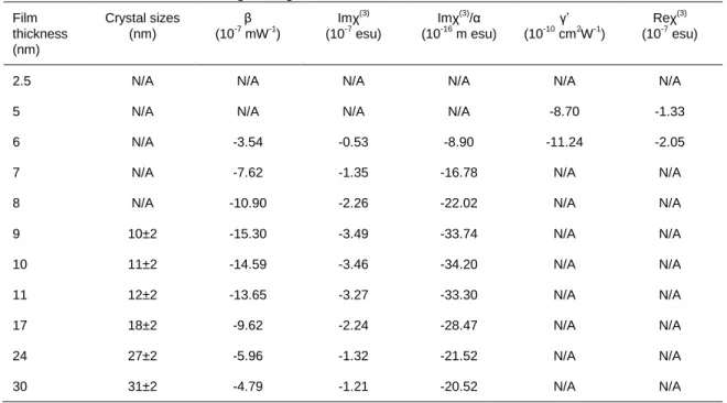
The nonlinear absorption coefficient (β), as well as the imaginary part of the third order
nonlinear susceptibility (Imχ(3)) have been determined by many experimental curves, following
the procedure described in the experimental section. Table 1 presents the nonlinear optical
parameters for all thin films investigated during this work. The Imχ(3) is also presented in Figure
5a as a function of the thin film thickness. In Figure 5b the figure of merit, defined as the Imχ(3)
divided by the linear absorption coefficient of the thin film layers at 1030 nm, is also presented.
It is obvious that the imaginary part of the third order nonlinear susceptibility and the figure of
merit obtain their maximum values for a film thickness of 9-11 nm. The nonlinear absorption
experimental curves shown in Figure 4a. It has to be noted that the choice of the thin film
thicknesses employed for this investigation have been gradually done during the studies in order
to allow a high precision determination of the highest nonlinear absorption that can be obtained
by the Sb2Te3 material.
In order to study the nonlinear refraction of the investigated materials “closed aperture” and
“divided” Z-scans have been recorded. The determination of the nonlinear refraction of the
Sb2Te3 layers is a very challenging procedure for the following reasons. For thin films thicker
than 6 nm the nonlinear absorption exhibits giant values and consequently it is dominating the
optical nonlinearities. In such cases the Reχ(3) becomes much lower than Imχ(3) and it cannot be
detected by the Z-scan technique.37 Decreasing the thickness can aid to surpass this difficulty,
however very low thicknesses result to negligible nonlinearities (both nonlinear refraction and
nonlinear absorption). For these reasons the nonlinear refractive parameters of the Sb2Te3
material at the ultrafast regime are unknown. These measurements can be accurately done for 5-6
nm thick layers. This is due to the fact that these layers exhibit low nonlinear absorption,
allowing a precise determination of the nonlinear refraction. A representative “divided” Z-scan
obtained for the 5 nm thin film layer with an incident laser intensity of 6 GW/cm2 is presented in Figure 4b. The “divided” Z-scan curves obtained during at this work show a peak-valley
configuration, which indicates a self-defocusing character and consequently negative Reχ(3)
values. The nonlinear refractive parameters have been determined in the case of the 5 and 6 nm
layers following the procedure shown in the experimental section and are shown in Table 1.
Similar thickness dependent studies of the Sb2Te3 material do not currently exist, despite the
importance of this material for applications. Our work demonstrates the significant dependence
examination of Table 1 one can identify five different regimes, which result to different NLO
behaviours. The first regime corresponds to very thin films (i.e. 2.5 nm) which exhibit negligible
nonlinear refraction and nonlinear absorption. The lack of high optical nonlinearities can be
attributed to the fact that in this case there is not sufficient matter to provide a uniform
crystallization of the layers. A second, different behaviour has been observed in the case of the 5
nm thick films. In that case there is a significant nonlinear refraction, while the thin films exhibit a negligible nonlinear absorption. The nonlinear refractive parameter ( ) and Reχ(3)
obtained in
this work are of the order of 10-9 cm2/W and 10-7 esu respectively. These values are significantly
high, showing that the Sb2Te3 material can exhibit a strong nonlinear refractive character if its
thickness is properly adjusted. It is interesting to make a comparison with the nonlinear
refraction values previously obtained for graphene layers, as they are currently a reference 2D
material for nonlinear optics. The published nonlinear optical properties of graphene vary a lot
due to an apparent strong dependence on the pulse duration, the excitation wavelength, the
repetition rate and the graphene preparation conditions. Chen et al.38 reported a nonlinear
refractive index of the order of 1.4x10⁻⁹ cm2/W, which is slightly higher than the values reported
in this work. The repetition rate employed by Chen et al. has been high (i.e. 80 MHz). In another
work similar values have been found (10-7~10-6 esu) by employing the same repetition rate.39
Very recently Karampitsos et al.40 have investigated graphene dispersions and have
demonstrated that the repetition rate of the laser plays a very important role on the NLO response
of graphene. Using a high repetition rate (i.e. 80 MHz) they have shown that thermal effects
dominate the nonlinearities. To avoid this fact the repetition rate has been kept low (i.e. 100 Hz)
during our work. Demetriou et al.41 investigated the optical nonlinearities of few-layer graphene
thermal effects arise they used a repetition rate of 1 kHz. The nonlinear refractive index obtained
using an excitation wavelength at 1150 nm is of the same order of magnitude with our reported
values for the Sb2Te3 layers. It has to be noted that the negative nonlinear refraction obtained
here (self-defocusing) is in accordance with several previous experimental and theoretical studies
on graphene systems.40–42 A negative nonlinear refraction has been also presented in Reference 43
in the case of another 2D material, black phosphorus, while the nonlinear refraction is 6-7 orders
of magnitude lower than that reported in this work.
A third regime can be observed in Table 1 for the 6 nm layers. In this case there is a
simultaneous existence of a nonlinear refraction and absorption. By further increasing the 2D
layer thickness a transition to a fourth regime occurs, where the nonlinear absorption reaches
record values, while gradually the nonlinear refraction disappears. This happens for thin films of
9-11 nm thickness. The nonlinear absorption coefficient has been found to be about an order of
magnitude higher than that published by Liu et al for the same material.44 The higher values
obtained here can be attributed to an enhancement of the nonlinear absorption achieved through
the thickness optimization that we present in this work and an annealing optimization that has
been previously detailed by our group.16 It has to be mentioned that the nonlinear absorption
coefficients found in this work are slightly lower than those that we have previously reported,
which is due to the shorter pulse duration of the laser system employed here (400 fs instead of
600 fs used in Reference 16). The pulse duration is well-known to have a significant impact on
the NLO response of 2D materials. For example Tang et al. have shown that a decrease of the
pulse duration from 1 ps to 100 fs can result to a decrease of the nonlinear absorption coefficient
of black phosphorus dispersions by about one order of magnitude.45 The giant nonlinear
detailed comparison and discussion of these nonlinear optical absorption efficiencies with
current state-of-the-art materials such as other chalcogenides,46,47 perovskites,48–50 graphene,51,52
carbon nanotubes53 and 2D α-Mo2C54 has been carried out by our group in Reference 16 (see
Table 1 therein). The nonlinear optical mechanism which gives rise to these giant β values is the
following. The Sb2Te3 material exhibits a very low bandgap of about 0.14-0.20 eV, which offers
to this material a broadband absorption character.16,33,34 The excitation wavelength employed in
this work (i.e. 1030 nm) excites the electrons from the valence band to the conduction band.
Increasing the laser intensity results to an increase of the number of carriers in the conduction
band. Since electrons are fermions, when all energy states are occupied, the Sb2Te3 material is
not able to absorb more light due to the Pauli blocking. This bleaching results to an increase of
the transmission and leads to high NLO responses. The significant contribution of this
mechanism to the NLO response of 2D materials has been previously demonstrated by our and
other scientific groups.1,4,16
Finally a fifth regime can be defined for thicker films. An increase of the film thickness over 10
nm results to a gradual decrease of the nonlinear absorption coefficients. For thicknesses over 24
nm lower optical nonlinearities are observed, while the optical losses of the layers become
significant.
The high dependence of the NLO response on the film thickness is attributed to the topological
insulator behaviour of the thin film layers. Even slight modifications of the optimal thicknesses
can result to a significant loss of the NLO performances. There is no evidence of this thickness
dependence in the literature so a further comparison with the literature is not feasible. However
thickness dependent studies have been performed for other 2D materials. Ahn et al. have recently
Optical Kerr gate experiments showing a high dependence on the number of graphene layers.39
Chen et al. studied the nonlinear refraction and the nonlinear absorption from monolayers to
multilayers in the case of graphene in the ultrafast regime.38 They demonstrated that the
nonlinear optical response is not proportional to the number of layers. This has been attributed to
the interlayer coupling. In another work it has been demonstrated that monolayer graphene acts
as a more effective saturable absorber than multilayer graphene.55 More specifically the
monolayer graphene has been found to provide a better pulse shaping ability, pulse stability and
output energy. On the contrary, as we show in this work, in the case of the Sb2Te3 material
higher thicknesses are needed to obtain giant optical nonlinearities. This is related to the different
nature of these two 2D materials. Graphene is obtained through the isolation of a single sheet of
graphite and it already has the necessary structure to obtain the NLO response. In the case of the
Sb2Te3 material, formation of nanocrystals is necessary to achieve high nonlinear absorption or
nonlinear refraction, which is obtained through a precise annealing of the deposited layers. Bao
et al.25 demonstrated that the saturation intensity of graphene systems can vary from 0.71 to 0.61
MW cm-2 by changing the number of layers from 3 ± 1 to 10 ± 1. They also found that the
modulation depth can be reduced from 66.5% to 6.2% by changing the number of graphene
layers. Other 2D materials have been also previously investigated. Thickness-dependent studies
have been also carried out in the case of SnS2 nanolayers in order to optimize their performance
for fibre lasers.56 In this case three different thicknesses have been studied and an increase of the
modulation depth with increasing the film thickness has been found, while the best performance
has been acquired by a 108.7 nm thick layer. In another work the nonlinear refraction and the
nonlinear absorption has been studied as a function of the size of black phosphorus nanosheets.43
part of the third order nonlinear optical susceptibilities by decreasing the nanosheets size. Tuo et
al studied 2D α-Mo2C crystals and find out that by changing the crystal thickness and the laser
intensity a significant tunability of the NLO parameters can be achieved.54
The results reported in this work are of significant importance for the field of nonlinear optics of
2D materials. They show that a precise tuning of the film thickness is necessary in order to
enhance the optical nonlinearities of the Sb2Te3 layers. On the contrary, avoiding such
adjustment can result to poor performances in terms of applications, as for example
mode-locking of fibre lasers. Moreover the thickness adjustment can result to a switching between
different NLO behaviours, so it can be employed in order to adapt the Sb2Te3 performance for
specific needs. More specifically, careful adjustment of the crystallized Sb2Te3 thickness can
provide a switching from a purely nonlinear refractive NLO regime to a regime where the
nonlinear absorption dominates the nonlinearities. Another important point has to be highlighted.
The nonlinear optical parameters found in this work demonstrate a non-monotonic dependence
on the film thickness. Such behaviour can only be detected by thorough NLO studies of many
different thin films. It is very possible that a similar behaviour will be unveiled for many other
2D materials by investigating a large number of samples, having appropriately adjusted
thicknesses.
CONCLUSIONS
The nonlinear optical properties of nanometer-thick 2D Sb2Te3 thin films have been studied by
the Z-scan technique employing 400 fs laser pulses at 1030 nm with a low repetition rate of 100
Hz in order to avoid the appearance of thermal effects. Significant NLO properties have been
order of 10-9 cm2/W has been obtained for 5-6 nm thick layers. This refraction if very high,
comparable with that of other state-of-the-art nonlinear optical materials. A giant nonlinear
absorption coefficient of the order of 10-6 m/W has been obtained for 9-11 nm thick films. The
nonlinear absorption dominates in that case the optical nonlinearities. These results show the
importance of the precise adjustment of the film thickness for mode locking and super-resolved
nanostructuring. We believe that these findings will trigger further research in the field of the
optical nonlinearities of 2D photonic materials.
METHODS
Sample Characterization. SEM analysis was performed with a Zeiss GeminiSEM 500
ultra-high resolution Field Emission Scanning Electron Microscope operating at 10 kV. A backscatter
electron detector was used for imaging in nanoscale. Grain sizes were measured using the Image
J software.
For TEM analysis, the samples were observed with a FEI Tecnaï G2 microscope operating at
200KV. This microscope is equipped with an X-Max Silicon Drift Detector (Oxford) which
allows Energy-dispersive X-ray spectroscopy measurements. The Cliff-Lorimer method as
implemented in the Aztec software package from Oxford is used for quantitative chemical
analysis.
Nonlinear Optical Studies. The nonlinear optical measurements have been performed by means
of the Z-scan technique. The Z-scan technique37 employs two different experimental arms, the so called “closed aperture” and “open aperture” Z-scans allowing a determination of the nonlinear
refraction and the nonlinear absorption of a material respectively. For the Z-scan studies an
provides pulses at a 40 MHz repetition rate. By means of a pulse picker and an acousto-optic
modulator, both integrated in the laser system, the repetition rate can be adjusted. For the Z-scan
measurements a 100 Hz repetition rate has been employed in order to avoid thermal effect
contribution to the measured nonlinear optical responses. The laser beam has been focused by a
10 cm focal length lens on the sample, which has been moved around the focal plane by means
of a computer controlled translation stage. The beam waist at the focal plane has been measured to be 20 μm.
The recorded “Closed aperture” and “Open aperture” Z-scans allow the determination of the real
and imaginary parts of the third order nonlinear optical susceptibility (Reχ(3)
and Imχ(3))
respectively. The nonlinear absorption coefficient β has been determined by fitting the “open aperture” Z-scan curves by means of the following equation:
(1)
where I0 is the on-axis irradiance at the focus, Leff is defined as Leff=(1-exp(-α0L))/α0 and α0 is the
linear absorption coefficient of the sample (at 1030 nm and at 515 nm respectively). The Imχ(3)
can be then calculated by means of the following equation:
(2)
where c is the speed of light in cm s-1, n0 is the linear refractive index and ω is the fundamental
frequency in cycles per sec.
The nonlinear refraction parameters have been obtained by dividing the “closed aperture”
Z-scans by the “open aperture” Z-Z-scans, obtaining the so-called “divided” Z-Z-scans. The “divided”
experimental analysis procedure previously detailed.57 The γ´ values have been determined as
follows:
(3)
where k is the wave number in vacuum, S is the linear transmittance of the aperture and ΔΤP-V is
the difference between the transmittance minima and maxima of the recorded experimental
curves.
The real part of the third order nonlinear optical susceptibility has been then obtained by means
of the following equation:
(4)
FIGURES
Figure 1
Figure 1. a-c) SEM images obtained in backscattered mode for the a) 10 nm b) 30 nm and c) 50
nm Sb2Te3 layers. d-f) Corresponding XRD diagrams ( = 0.15418 nm) for the d) 10 nm e) 30 nm f) 50 nm samples.
Figure 2
Figure 2. Cross-sectional STEM bright field images for the a) 10 nm and b) 30 nm annealed
Sb2Te3 layers. The rectangle indicates the area scanned by the beam for the EDX analysis.
EDX Spectra obtained for the c) 10 nm and d) 30 nm samples. The Sb(K) and Te(K) ionization peaks used for quantitative analysis are located at 26.4 keV and 27.4 keV.
Figure 3
Figure 3. a) Transmittance and b) Reflectance spectra for different film thicknesses. c)
Transmittance, reflectance and absorption at 1030 nm as a function of the Sb2Te3 thickness. Spectral dependence of the d) Real and e) Imaginary parts of the refractive index for different film thicknesses. f) Real and imaginary parts of the refractive index at 1030 nm as a function of the film thickness for all the investigated layers.
Figure 4
Figure 4. a) “Open aperture” Z-scan curves for three different Sb2Te3 thicknesses. b) “Divided” Z-scan obtained for the 5 nm thick layer.
Figure 5
TABLES
Table 1. Determined nonlinear optical parameters (1030 nm, 400 fs)
Film thickness (nm) Crystal sizes (nm) β (10-7 mW-1) Imχ(3) (10-7 esu) Imχ(3)/α (10-16 m esu) γ’ (10-10 cm2W-1) Reχ(3) (10-7 esu)
2.5 N/A N/A N/A N/A N/A N/A
5 N/A N/A N/A N/A -8.70 -1.33
6 N/A -3.54 -0.53 -8.90 -11.24 -2.05 7 N/A -7.62 -1.35 -16.78 N/A N/A 8 N/A -10.90 -2.26 -22.02 N/A N/A 9 10±2 -15.30 -3.49 -33.74 N/A N/A 10 11±2 -14.59 -3.46 -34.20 N/A N/A 11 12±2 -13.65 -3.27 -33.30 N/A N/A 17 18±2 -9.62 -2.24 -28.47 N/A N/A 24 27±2 -5.96 -1.32 -21.52 N/A N/A 30 31±2 -4.79 -1.21 -20.52 N/A N/A ASSOCIATED CONTENT Supporting Information.
SEM image of a 7 nm Sb2Te3 layer. “Open aperture” Z-scan curves of an amorphous and annealed layer (same thickness). “Open aperture” Z-scans of different thickness Sb2Te3 layers. Repeatability of the Z-scan measurements.
AUTHOR INFORMATION
Corresponding Author
*E-mail: [email protected]
R.N.V. and C.M performed the nonlinear optical studies. F.L. carried out the determination of
the refractive index of the thin films. A.C. and M.C. performed the SEM, TEM and EDX
characterizations and analysed the results. C.P.P performed the X-Ray Diffraction studies and
analysed the experimental findings. J.L. deposited the thin film layers and performed the
spectrophotometric studies. J.Y.N. and K.I. supervised the project and wrote the manuscript with
input from all authors.
NOTES
The authors declare no competing financial interest.
ACKNOWLEDGMENTS
The authors would like to thank Dr. Jean-Benoît Claude for his participation in the surface
morphology studies. The authors acknowledge financial support from the French National
Research Agency (ANR-19-CE09-0002-01), from the Ministry for Armed Forces (DGA) and
Aix-Marseille University.
REFERENCES
(1) You, J. W.; Bongu, S. R.; Bao, Q.; Panoiu, N. C. Nonlinear Optical Properties and
Applications of 2D Materials: Theoretical and Experimental Aspects. Nanophotonics 2019, 8,
(2) Yamashita, S. Nonlinear Optics in Carbon Nanotube, Graphene, and Related 2D
Materials. APL Photon. 2019, 4, 034301.
(3) Liu, X.; Guo, Q.; Qiu, J. Emerging Low-Dimensional Materials for Nonlinear Optics and
Ultrafast Photonics. Adv. Mater. 2017, 29, 1605886.
(4) Liu, W.; Liu, M.; Liu, X.; Wang, X.; Deng, H.; Lei, M.; Wei, Z.; Wei, Z. Recent
Advances of 2D Materials in Nonlinear Photonics and Fiber Lasers. Adv. Optical Mater. 2020, 8,
1901631.
(5) Guo, B.; Xiao, Q.; Wang, S.; Zhang, H. 2D Layered Materials: Synthesis, Nonlinear
Optical Properties, and Device Applications. Laser Photonics Rev. 2019, 13, 1800327.
(6) Autere, A.; Jussila, H.; Dai, Y.; Wang, Y.; Lipsanen, H.; Sun, Z. Nonlinear Optics Based
on Two-dimensional Layered Materials. Adv. Mater. 2018, 30, 1705963.
(7) Wang, G.; Baker‐Murray, A. A.; Blau, W. J. Saturable Absorption in 2D Nanomaterials and Related Photonic Devices. Laser Photonics Rev. 2019, 13, 1800282.
(8) Wu, L.; Dong, Y.; Zhao, J.; Ma, D.; Huang, W.; Zhang, Y.; Wang, Y.; Jiang, X.; Xiang,
Y.; Li, J.; Feng, Y.; Xu, J.; Zhang, H. Kerr Nonlinearity in 2D Graphdiyne for Passive Photonic
Diodes. Adv. Mater. 2019, 31, 1807981.
(9) Ge, Y.; Zhu, Z.; Xu, Y.; Chen, Y.; Chen, S.; Liang, Z.; Song, Y.; Zou, Y.; Zeng, H.; Xu,
S.; Zhang, H.; Fan, D. Broadband Nonlinear Photoresponse of 2D TiS2 for Ultrashort Pulse
(10) Jiang, X.; Zhang, L.; Liu, S.; Zhang, Y.; He, Z.; Li, W.; Zhang, F.; Shi, Y.; Lü, W.; Li,
Y.; Wen, Q.; Li, J.; Feng, J.; Ruan, S.; Zeng, Y.-J.; Zhu, X.; Lu, Y.; Zhang, H. Ultrathin
Metal-Organic Framework: An Emerging Broadband Nonlinear Optical Material for Ultrafast
Photonics. Adv. Optical Mater. 2018, 6, 1800561.
(11) Lu, L.; Tang, X.; Cao, R.; Wu, L.; Li, Z.; Jing, G.; Dong, B.; Lu, S.; Li, Y.; Xiang, Y.; Li,
J.; Fan, D.; Zhang, H. Broadband Nonlinear Optical Response in Few-Layer Antimonene and
Antimonene Quantum Dots: A Promising Optical Kerr Media with Enhanced Stability. Adv.
Optical Mater. 2017, 5, 1700301.
(12) Jiang, X.; Kuklin, A. V.; Baev, A.; Ge, Y.; Ågren, H.; Zhang, H.; Prasad, P. N.
Two-Dimensional MXenes: From Morphological to Optical, Electric, and Magnetic Properties and
Applications. Phys. Rep. 2020, 848, 1–58.
(13) Liu, W.; Zhu, Y.-N.; Liu, M.; Wen, B.; Fang, S.; Teng, H.; Lei, M.; Liu, L.-M.; Wei, Z.
Optical Properties and Applications for MoS2-Sb2Te3-MoS2 Heterostructure Materials. Photonics
Res. 2018, 6, 220-227.
(14) Wang, K.; Szydłowska, B. M.; Wang, G.; Zhang, X.; Wang, J. J.; Magan, J. J.; Zhang, L.;
Coleman, J. N.; Wang, J.; Blau, W. J. Ultrafast Nonlinear Excitation Dynamics of Black
Phosphorus Nanosheets from Visible to Mid-Infrared. ACS Nano 2016, 10, 6923–6932.
(15) Zhang, H.; Liu, C.-X.; Qi, X.-L.; Dai, X.; Fang, Z.; Zhang, S.-C. Topological Insulators
in Bi2Se3, Bi2Te3 and Sb2Te3 with a Single Dirac Cone on the Surface. Nat. Phys. 2009, 5, 438–
(16) Moisset, C.; Verrone, R.-N.; Bourgade, A.; Zeweldi, G. T.; Minissale, M.; Gallais, L.;
Perrin-Pellegrino, C.; Akhouayri, H.; Lumeau, J.; Natoli, J.-Y.; Iliopoulos, K. Giant Ultrafast
Optical Nonlinearities of Annealed Sb2Te3 Layers. Nanoscale Adv. 2020, 2, 1427-1430.
(17) Moisset, C.; Bourgade, A.; Lumeau, J.; Lemarchand, F.; Perrin-Pellegrino, C.;
Akhouayri, H.; Natoli, J.-Y.; Iliopoulos, K. Saturable Absorption Optimization of Silica
Protected Thin Sb2Te3 Layers towards Super-Resolution Applications. Opt. Mater. 2018, 86, 7–
11.
(18) Wei, J.; Liu, S.; Geng, Y.; Wang, Y.; Li, X.; Wu, Y.; Dun, A. Nano-Optical Information
Storage Induced by the Nonlinear Saturable Absorption Effect. Nanoscale 2011, 3, 3233-3237.
(19) Liu, J.; Liu, S.; Wei, J. Origin of the Giant Optical Nonlinearity of Sb2Te3 Phase Change
Materials. Appl. Phys. Lett. 2010, 97, 261903.
(20) Liu, S.; Wei, J.; Gan, F. Nonlinear Absorption of Sb-Based Phase Change Materials Due
to the Weakening of the Resonant Bond. Appl. Phys. Lett. 2012, 100, 111903.
(21) Boguslawski, J.; Sotor, J.; Sobon, G.; Tarka, J.; Jagiello, J.; Macherzynski, W.; Lipinska,
L.; Abramski, K. M. Mode-Locked Er-Doped Fiber Laser Based on Liquid Phase Exfoliated
Sb2Te3 Topological Insulator. Laser Phys. 2014, 24, 105111.
(22) Kowalczyk, M.; Bogusławski, J.; Zybała, R.; Mars, K.; Mikuła, A.; Soboń, G.; Sotor, J.
Sb2Te3-Deposited D-Shaped Fiber as a Saturable Absorber for Mode-Locked Yb-Doped Fiber
(23) Liu, W.; Pang, L.; Han, H.; Tian, W.; Chen, H.; Lei, M.; Yan, P.; Wei, Z. Generation of
Dark Solitons in Erbium-Doped Fiber Lasers Based Sb2Te3 Saturable Absorbers. Opt. Express
2015, 23, 26023-26031.
(24) Liu, W.; Pang, L.; Han, H.; Tian, W.; Chen, H.; Lei, M.; Yan, P.; Wei, Z. 70-Fs
Mode-Locked Erbium-Doped Fiber Laser with Topological Insulator. Sci. Rep. 2016, 6, 19997.
(25) Bao, Q.; Zhang, H.; Wang, Y.; Ni, Z.; Yan, Y.; Shen, Z. X.; Loh, K. P.; Tang, D. Y.
Atomic-Layer Graphene as a Saturable Absorber for Ultrafast Pulsed Lasers. Adv. Funct. Mater.
2009, 19, 3077–3083.
(26) Goldstein, J. I.; Newbury, D. E.; Michael, J. R.; Ritchie, N. W. M.; Scott, J. H. J.; Joy, D.
C. Scanning Electron Microscopy and X-Ray Microanalysis; Springer New York, fourth edition,
2018.
(27) Wang, Q.; Liu, B.; Xia, Y.; Zheng, Y.; Huo, R.; Zhu, M.; Song, S.; Lv, S.; Cheng, Y.;
Song, Z.; Feng, S. Characterization of Cr-Doped Sb2Te3 Films and Their Application to
Phase-Change Memory. Phys. Status Solidi RRL 2015, 9, 470–474.
(28) Yin, Y.; Sone, H.; Hosaka, S. Characterization of Nitrogen-Doped Sb2Te3 Films and
Their Application to Phase-Change Memory. J. Appl. Phys. 2007, 102, 064503.
(29) Liu, T.; Deng, H.; Cao, H.; Zhou, W.; Zhang, J.; Liu, J.; Yang, P.; Chu, J. Structural,
Optical and Electrical Properties of Sb2Te3 Films Prepared by Pulsed Laser Deposition. J. Cryst.
Growth 2015, 416, 78–81.
(31) Lv, B.; Hu, S.; Li, W.; Di, X.; Feng, L.; Zhang, J.; Wu, L.; Cai, Y.; Li, B.; Lei, Z.
Preparation and Characterization of Sb2Te3 Thin Films by Coevaporation. Int. J. Photoenergy
2010, 2010, 1–4.
(32) Cullity, B. D.; Stock, S. R. Elements of X-Ray Diffraction; Third Edition, Prentice Hall,
2001.
(33) Park, J.-W.; Eom, S. H.; Lee, H.; Da Silva, J. L. F.; Kang, Y.-S.; Lee, T.-Y.; Khang, Y.
H. Optical Properties of Pseudobinary GeTe, Ge2Sb2Te5, GeSb2Te4, GeSb4Te7, and Sb2Te3 from
Ellipsometry and Density Functional Theory. Phys. Rev. B 2009, 80, 115209.
(34) Olson, J. K.; Li, H.; Ju, T.; Viner, J. M.; Taylor, P. C. Optical Properties of Amorphous
GeTe, Sb2Te3, and Ge2Sb2Te5: The Role of Oxygen. J. Appl. Phys. 2006, 99, 103508.
(35) Gao, L.; Lemarchand, F.; Lequime, M. Comparison of Different Dispersion Models for
Single Layer Optical Thin Film Index Determination. Thin Solid Films 2011, 520, 501–509.
(36) Kuwahara, M.; Endo, R.; Tsutsumi, K.; Morikasa, F.; Tsuruoka, T.; Fukaya, T.; Suzuki,
M.; Susa, M.; Endo, T.; Tadokoro, T. Approach for Measuring Complex Refractive Index of
Molten Sb2Te3 by Spectroscopic Ellipsometry. Applied Physics Letters 2012, 100, 101910.
(37) Sheik-Bahae, M.; Said, A. A.; Wei, T.-H.; Hagan, D. J.; Van Stryland, E. W. Sensitive
Measurement of Optical Nonlinearities Using a Single Beam. IEEE J. Quantum Electron. 1990,
(38) Chen, W.; Wang, G.; Qin, S.; Wang, C.; Fang, J.; Qi, J.; Zhang, X.; Wang, L.; Jia, H.;
Chang, S. The Nonlinear Optical Properties of Coupling and Decoupling Graphene Layers. AIP
Adv. 2013, 3, 042123.
(39) Ahn, K. J.; Gwak, J. Y.; Lee, B. J.; Choi, S. Y.; Kim, M. H.; Baek, I. H.; Jeong, Y. U.;
Rotermund, F. Wavelength and Fluence-Dependent Third-Order Optical Nonlinearity of Mono-
and Multi-Layer Graphene. Appl. Optics 2017, 56, 9920-9924.
(40) Karampitsos, N.; Kyrginas, D.; Couris, S. On the Measurement of the Nonlinear Optical
Response of Graphene Dispersions Using fs Lasers. Opt. Lett. 2020, 45, 1814-1817.
(41) Demetriou, G.; Bookey, H. T.; Biancalana, F.; Abraham, E.; Wang, Y.; Ji, W.; Kar, A. K.
Nonlinear Optical Properties of Multilayer Graphene in the Infrared. Opt. Express 2016, 24,
13033-13043.
(42) Ooi, K. J. A.; Ang, L. K.; Tan, D. T. H. Waveguide Engineering of Graphene’s
Nonlinearity. Appl. Phys. Lett. 2014, 105, 111110.
(43) Xu, Y.; Jiang, X.-F.; Ge, Y.; Guo, Z.; Zeng, Z.; Xu, Q.-H.; Zhang, H.; Yu, X.-F.; Fan, D.
Size-Dependent Nonlinear Optical Properties of Black Phosphorus Nanosheets and Their
Applications in Ultrafast Photonics. J. Mater. Chem. C 2017, 5, 3007–3013.
(44) Liu, C.; Cheng, L.; Yuan, Y.; Su, J.; Zhang, X.; Li, X.; Zhao, H.; Zhang, H.; Zheng, Y.;
Li, J. Contrastive Investigation on Linear Optical Properties and Nonlinear Absorption Behaviors
(45) Tang, S.; He, Z.; Liang, G.; Chen, S.; Ge, Y.; Sang, D. K.; Lu, J.; Lu, S.; Wen, Q.;
Zhang, H. Pulse Duration Dependent Nonlinear Optical Response in Black Phosphorus
Dispersions. Opt. Commun. 2018, 406, 244–248.
(46) Fang, J.; Wang, J.; Cao, X.; Man, Y.; Liu, C.; Cheng, L.; Zhang, X.; Zhao, H.; Zhang, H.;
Li, J. Thickness Dependence of a Giant Nonlinear Saturable Absorption Response in GeSb4Te7
Thin Films. J. Phys. Commun. 2018, 2, 015009.
(47) Wang, Y.; Liu, S.; Yuan, J.; Wang, P.; Chen, J.; Li, J.; Xiao, S.; Bao, Q.; Gao, Y.; He, J.
Ultra-Broadband Nonlinear Saturable Absorption for Two-Dimensional Bi2TexSe3−x Nanosheets.
Sci. Rep. 2016, 6, 33070.
(48) Kalanoor, B. S.; Gouda, L.; Gottesman, R.; Tirosh, S.; Haltzi, E.; Zaban, A.; Tischler, Y.
R. Third-Order Optical Nonlinearities in Organometallic Methylammonium Lead Iodide
Perovskite Thin Films. ACS Photonics 2016, 3, 361–370.
(49) Li, J.; Dong, H.; Xu, B.; Zhang, S.; Cai, Z.; Wang, J.; Zhang, L. CsPbBr3 Perovskite
Quantum Dots: Saturable Absorption Properties and Passively Q-Switched Visible Lasers.
Photonics Res. 2017, 5, 457-460.
(50) Li, P.; Chen, Y.; Yang, T.; Wang, Z.; Lin, H.; Xu, Y.; Li, L.; Mu, H.; Shivananju, B. N.;
Zhang, Y.; Zhang, Q.; Pan, A.; Li, S.; Tang, D.; Jia, B.; Zhang, H.; Bao, Q. Two-Dimensional
CH3NH3PbI3 Perovskite Nanosheets for Ultrafast Pulsed Fiber Lasers. ACS Appl. Mater.
(51) Kumar, S.; Anija, M.; Kamaraju, N.; Vasu, K. S.; Subrahmanyam, K. S.; Sood, A. K.;
Rao, C. N. R. Femtosecond Carrier Dynamics and Saturable Absorption in Graphene
Suspensions. Appl. Phys. Lett. 2009, 95, 191911.
(52) He, M.; Quan, C.; He, C.; Huang, Y.; Zhu, L.; Yao, Z.; Zhang, S.; Bai, J.; Xu, X.
Enhanced Nonlinear Saturable Absorption of MoS2/Graphene Nanocomposite Films. J. Phys.
Chem. C 2017, 121, 27147–27153.
(53) Tatsuura, S.; Furuki, M.; Sato, Y.; Iwasa, I.; Tian, M.; Mitsu, H. Semiconductor Carbon
Nanotubes as Ultrafast Switching Materials for Optical Telecommunications. Adv. Mater. 2003,
15, 534–537.
(54) Tuo, M.; Xu, C.; Mu, H.; Bao, X.; Wang, Y.; Xiao, S.; Ma, W.; Li, L.; Tang, D.; Zhang,
H.; Premaratne, M.; Sun, B.; Cheng, H.-M.; Li, S.; Ren, W.; Bao, Q. Ultrathin 2D Transition
Metal Carbides for Ultrafast Pulsed Fiber Lasers. ACS Photonics 2018, 5, 1808–1816.
(55) Bao, Q.; Zhang, H.; Ni, Z.; Wang, Y.; Polavarapu, L.; Shen, Z.; Xu, Q.-H.; Tang, D.;
Loh, K. P. Monolayer Graphene as a Saturable Absorber in a Mode-Locked Laser. Nano Res.
2011, 4, 297–307.
(56) Liu, W.; Liu, M.; Wang, X.; Shen, T.; Chang, G.; Lei, M.; Deng, H.; Wei, Z.; Wei, Z.
Thickness-Dependent Ultrafast Photonics of SnS2 Nanolayers for Optimizing Fiber Lasers. ACS
Appl. Nano Mater. 2019, 2, 2697–2705.
(57) Iliopoulos, K.; Potamianos, D.; Kakkava, E.; Aloukos, P.; Orfanos, I.; Couris, S. Ultrafast