HAL Id: hal-01968187
https://hal.laas.fr/hal-01968187
Submitted on 2 Jan 2019
HAL is a multi-disciplinary open access
archive for the deposit and dissemination of
sci-entific research documents, whether they are
pub-lished or not. The documents may come from
teaching and research institutions in France or
abroad, or from public or private research centers.
L’archive ouverte pluridisciplinaire HAL, est
destinée au dépôt et à la diffusion de documents
scientifiques de niveau recherche, publiés ou non,
émanant des établissements d’enseignement et de
recherche français ou étrangers, des laboratoires
publics ou privés.
Thickness limitation of band to band tunneling process
in InGaAs/GaAsSb type-II tunnel junctions designed for
multijunction solar cells
Kevin Louarn, Y Claveau, Chantal Fontaine, Alexandre Arnoult, Ludovic
Marigo-Lombart, Inès Massiot, F. Piquemal, A. Bounouh, N. Cavassilas,
Guilhem Almuneau
To cite this version:
Kevin Louarn, Y Claveau, Chantal Fontaine, Alexandre Arnoult, Ludovic Marigo-Lombart, et al..
Thickness limitation of band to band tunneling process in InGaAs/GaAsSb type-II tunnel junctions
designed for multijunction solar cells. ACS Applied Energy Materials, ACS, 2019, 2 (2), pp.1149-1154.
�10.1021/acsaem.8b01700�. �hal-01968187�
1
Thickness limitation of band to band tunneling process in InGaAs/GaAsSb type-II tunnel junctions designed for multijunction solar cells
K. Louarn1,2, Y. Claveau3, C. Fontaine1, A. Arnoult1, L. Marigo-Lombart1, I. Massiot1, F. Piquemal2, A. Bounouh4, N. Cavassilas3 and G. Almuneau*,1
1
LAAS-CNRS, Université de Toulouse, 7 avenue du Colonel Roche, 31400 Toulouse, France
2
LNE, 29 Avenue Roger Hennequin, F-78197 Trappes, France
3
Aix Marseille Université, CNRS, Université de Toulon, IM2NP UMR 7334, 13397, Marseille, France
4
CEA LIST, Centre d'études, F-91400, Gif-sur-Yvette, France
*
E-mail : almuneau@laas.fr
ABSTRACT: This article reports on the impact of the thickness and/or the composition on the performance of type-II n+ InGaAs / p+ GaAsSb tunnel junctions. The InGaAs/GaAsSb staggered band-offset heterojunction is expected to improve tunneling properties. Devices have been grown by molecular beam epitaxy with various thicknesses and/or Sb and In concentrations. For thin elastically strained type-II tunnel junctions, the electrical characteristics exhibit degraded transport performances compared to the reference p+ GaAs / n+ GaAs tunnel junction structures, while much better tunneling peak currents are achieved with strain-relaxed thick type-II tunnel junctions. Based on a theoretical analysis of the local density of states and the band-edges profiles of the type II tunnel junctions, we propose a suitable design for type II tunnel junctions with high tunneling current density towards their use in multijunction solar cells.
Keywords: III-V Semiconductors, Gallium Arsenide Based cells, Multijunction Solar Cell, Epitaxy, Tunnel Junction
1 INTRODUCTION
Tunnel Junctions (TJs) are key devices for monolithic multi-junction solar cells (MJSCs), in which they interconnect adjacent sub-cells. Each sub-cell of Multi-Junction Solar Cells (MJSCs) is designed to absorb a specific range of the solar spectrum. Thus, the absorption spectral response of the whole device is extended whilst thermalization losses are reduced, enabling to reach conversion efficiencies as high as 46% (1).
A TJ must meet four main criteria in order to perform as an efficient interconnection between adjacent sub-cells: (i) Its peak tunneling current density (Jpeak) must be higher than the photocurrent density of
the MJSCs; (ii) it should have an intrinsic electrical resistivity as low as possible; (iii) it should be transparent on the spectral range of interest for the photons to be absorbed in the underlying subcells. Moreover, in the case of TJ shaped with mismatched layers, (iv) the latter layers should be elastically strained in order to avoid dislocations that could propagate in upper sub-cells. The photocurrent density is around 15 mA/cm² at 1 sun for most of the existing designs of MJSCs (wafer bonding (1), dilute nitride (2), metamorphic (3)) and can reach values as high as 15 A/cm² at 1000 suns. To be suited for their use in MJSCs, TJs must therefore exhibit Jpeak significantly
higher than 15 A/cm² in order to have a low electrical resistivity at their working point. In order to evaluate and compare the electrical performances of the TJs, we focus only on the Jpeak value and not on the intrinsic
resistance. Indeed, the J-V characteristic of a low resistive TJ is dominated by the series parasitic resistances of the global device (mostly due to the metal/semiconductor interfaces) and thus decorrelated to the tunneling junction. Such parasitic resistances have a huge impact on the apparent resistance extracted from the experimental J-V characteristic but do not affect the Jpeak value, as presented in (4).
The usual way to get low resistive TJs with high Jpeak values is to use highly doped materials. Although
it is easy to get high doping levels in p-Type GaAs with C or Be dopants, the task is more complicated for n-type GaAs. It is indeed well known that the Si dopant in GaAs suffers from compensation and saturation issues, which limits the n-doping level to ~7x1018 cm-3 (5) (6) and thus the performance of the GaAs TJs. The use of Te for n-doping rather than Si enables to get high doping levels in the range of ~3x1019 cm-3 which
is required for strong tunneling currents. For example, AlGaAs:C/GaInP:Te or AlGaAs:C/GaAs:Te have been recently developed by metal organic vapor phase epitaxy (MOVPE) with peak tunneling current density up to 10 kA/cm² (7). Unfortunately, the Te dopant is not commonly used for n-doped MBE-grown devices, and other MBE approaches to exceed the saturation limit of Si dopant in GaAs have to be considered. The use of specific MBE growth conditions, nominally at a low temperature and a low growth rate, have been shown to enable reaching n-doping levels as high as ~2x1019 cm-3 (8). Jpeak values up to 1800 A/cm² for
GaAs TJs grown at 400°C have thus been demonstrated (9).
An alternative approach to improve the electrical properties of TJs is to increase the direct band to band tunneling (DBBT) probability thanks to the band-offset engineering capabilities offered by the type-II InGaAs/GaAsSb staggered-band heterojunctions. As pictured in Fig. 1, the tunneling distance in the TJ is significantly reduced in the case of a type-II band offset compared to a usual GaAs tunnel homojunction. This results in a significant increase of the tunneling current density which is directly linked to the tunneling probability and the density of states (DOS) involved in the tunneling process (10). High Jpeak values up to 1500
A/cm² have already been achieved (11) with such InGaAs/GaAsSb metamorphic type II TJs. An even higher Jpeak of 12 kA/cm² was reached for a
pseudomorphic InGaAs/GaAsSb type-II TJ for VCSEL applications (12). Although such type II TJs are
2 interesting for their electrical properties, the use of lattice-mismatched GaAsSb and InGaAs alloys with a lower bandgap than GaAs impacts the TJs structural and optical properties. Therefore, the thicknesses and the In and Sb concentrations of the TJ layers have to be carefully chosen to keep the positive impact of the type II heterojunction on the tunneling current. The use of low thicknesses and low In and Sb concentrations will fulfill the optical and structural criteria above mentionned.
In this work, we investigate the impact of the thicknesses and the In and Sb concentrations of the InGaAs and GaAsSb layers on the electrical properties of the type II TJs in order to find a TJ design that meets all the requirements for MJSCs. The study is led on a set of 7 MBE-grown InxGa1-xAs:Si / GaAs1-ySby:CTJ
samples with different concentrations of x=y= 0, 0.05 and 0.12 and various thicknesses. To control the structural properties of the two mismatched ternary layers during the MBE growth, we used a home-built optical setup enabling the in-situ real-time monitoring of the wafer curvature; this allows us to check if the growth is kept pseudomorphic or is strain-relaxed. The results of J-V measurements performed on thin (14-20 nm) and thick (100 nm) type-II TJs as well as on GaAs reference TJs with equivalent thicknesses are presented, indicating that the electrical behavior of the thick type-II TJs is much better than their thin type-II and Type-I counterparts. An analysis of the local density of states (LDOS) performed with non-equilibrium Green’s Functions (NEGF) is proposed to understand the impact of the thickness on the tunneling mechanisms. Finally, we propose an alternative design for type II TJs that fulfill all the requirements for MJSCs.
Fig. 1: Simulated band edge profiles at thermal
equilibrium of type-II p++ GaAs0.9Sb0.1 / n++
In0.1Ga0.9As (blue curve) and GaAs (black curve) TJs,
showing the reduced tunneling distance due to the type-II staggered band configuration with In- and Sb- containing alloys. Doping levels are kept constant in both structures. Band offsets of the InGaAs/GaAsSb heterojunction are taken from (11).
2 EXPERIMENTS
2.1 MBE growth of the InxGa1-xAs/GaAs1-ySby TJs
A set of seven MBE-grown TJ samples have been fabricated on n-type (001) GaAs substrates in a Riber 412 growth chamber. Si and C (CBr4 injector) elements
are used as n and p-type dopants, respectively. The TJ typical structure is shown in Fig. 2. Different thicknesses are used for the type-II heterojunction within the different samples. We optimized MBE growth conditions to exceed the Si saturation limits in GaAs with a growth temperature of 460°C and a growth rate of 0.5 µm/h. With such growth conditions, a n-type doping level as high as 1.3x1019 cm-3 with Si is achieved for the cathode of the TJ whereas the p-type doping level of the TJ anode is set to 1020 cm-3. In this study, relatively low In and Sb concentration are used; so we assumed that the electrical activation of the Si and C doping species are similar for GaAsSb and InGaAs as for GaAs. The p- and n-doping levels are thus considered to be equivalent in the GaAs TJs and in the InGaAs/GaAsSb TJs. In order to mimic the environment in which the TJ will be placed within a MJSC, the TJ is surrounded by two GaAs layers with lower doping (2x1018 cm-3) that model the subcells. A highly p-doped GaAs cap layer is grown on top of the structure to ensure a good ohmic contact. The In and Sb concentrations are kept identical for all the devices (xIn=ySb), to provide the similar conduction and valence
band offsets. Two different concentration sets xIn/Sb=0.05 and 0.12, have been investigated in addition
to the reference GaAs TJ (xIn/Sb=0). The samples are
labeled as follows: “TJ-X%-thin” or “-thick”, with X denoting the In and Sb composition percentages with X=0 for GaAs.
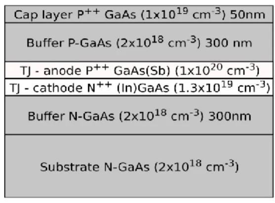
Fig. 2: Schematic structure of the MBE-grown TJ
devices. In and Sb contents of the anode and cathode as well as their thicknesses are varied across different samples.
The design criterion for the “thin” TJs is defined to be below the critical thickness for strain relaxation determined by the model of Matthews and Blakeslee (13) beyond which the misfit dislocations are generated in the layers. It gives thicknesses below 20 nm for TJ-5%-thin and 14 nm for TJ-12%-thin. The thickness of the “thick” TJs, 100 nm, largely exceeds this critical thickness, and is equally distributed between the cathode and anode. The samples properties are summarized in Table 1.
3 Name N/P doping level (cm-3) In/Sb content Anode /Cathode thickness TJ-0%-thin 1.3x10¹⁹/1x1020 0/0 % 15/15 nm TJ-0%-thick 1.3x10¹⁹/1x1020 0/0 % 50/50 nm TJ-5%-thin 1.3x10¹⁹/1x1020 5/5 % 10/10 nm TJ-5%-thick 1.3x10¹⁹/1x1020 5/5 % 50/50 nm TJ-12%-thin 1.3x10¹⁹/1x1020 12/12 % 7/7 nm TJ-12%-thick 1.3x10¹⁹/1x1020 12/12 % 50/50 nm
Table 1: List of the samples presented in this work.
The wafer curvature is monitored in real time, and thereby the strain state of the layers, in order to detect any strain relaxation in the layers, as already published with other methods (14) (15). The evolution of the incremental stress (.hf) linked to the wafer curvature
through the Stoney equation, is plotted as a function of the grown film thickness (hf). When the growth is
pseudomorphic, the variation of the incremental stress is linear, and the slope is equal to the stress () experienced by the elastically-strained growing layer.
2.2 Fabrication of the test devices
30 µm-diameter circular diodes were then fabricated on the MBE-grown samples using a self-aligned process described in (16). An alloyed AuGe/Ni/Au contact is deposited on the n-doped substrate backside followed by a rapid thermal annealing carried out at 450°C for 90s. The diodes are fabricated using self-aligned lift-off process consisting of a photolithography, dry etching and deposition by low temperature chemical vapor deposition (ICP-PECVD) of a SiOx layer to isolate the mesa sidewalls.
After getting rid of the SiOx/resist from the top of the
mesa, a Ti/Au top-contact is then deposited on the cap layer to make the front contact.
3. RESULTS
3.1 Structural properties of the TJs
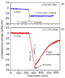
The “Thin” type-II TJs are supposed to exhibit excellent structural properties since their thickness is below the theoretical relaxation thickness (13). The structure should then be dislocation-free. As shown in
Fig. 3a, by the in-situ wafer curvature measurements
on the sample TJ-12%-thin (blue curve), the epitaxial growth of 7 nm of GaAs0.88Sb0.12 and 7 nm of
In0.12Ga0.88As is pseudomorphic. Indeed, the variation
of the incremental stress (.hf) is linear. Note that it has
a negative value because both the In- and Sb-containing alloy layers are compressively strained when grown on GaAs. The incremental stress is stabilized at the end of the InGaAs/GaAsSb heterostructure growth and during the growth of the upper GaAs layer. This confirms that the InGaAs/GaAsSb layers growth is pseudomorphic. Otherwise, the GaAs layer would have experienced a tensile strain, and the value of the incremental stress would have been positive.
That is what occurs for the “thick” type-II TJ-12% structure. As shown in Fig. 3b, in-situ wafer curvature measurements indicate that strain relaxation occurs during the growth of the GaAs0.88Sb0.12 layer. Upon
relaxation, the incremental stress variation reverses abruptly from a negative to a positive slope, and this trend is pursued during the subsequent GaAs growth. This behavior indicates the generation of dislocations, resulting in a poor structural quality for the TJ structure. The epitaxial growth of this material was then metamorphic.
In the case of the two TJs with 5% In and Sb content with a lower lattice-mismatch to the substrate, the in-situ wafer curvature monitoring (not presented here) shows that the MBE growth remains always pseudomorphic even for the thick structure.
It is worth noting that the pseudomorphic growth is preserved for an InGaAs layer thickness of about 100 nm and 60 nm for the TJ-5% and -12% respectively. These observed critical thicknesses are thus much higher than the ones given by the Matthews’ formula. It can be explained by the use of a low growth temperature which differs from the thermodynamic equilibrium conditions considered in Matthews’ model. It may also stem from the doping impurities contained in the layers which may affect the mechanical properties of the semiconductor (17).
Fig. 3: In-situ wafer curvature measurements during
MBE growth of sample TJ-12%-thin (a) and sample TJ-12%-thick (b). This “thick” sample exhibits strain relaxation appearing during the growth of the GaAsSb layer.
3.2 J-V characteristics of the devices
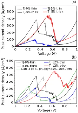
The J-V measurements of the samples with 5% In and Sb content are presented in Fig. 4.a and the ones of samples with 12% In and Sb contents are presented in
Fig. 4.b. The J-V measurements of the reference GaAs
TJs are plotted in black in both figures for comparison. The J-V characteristics of all TJs exhibit the well-known measurement instabilities in the Negative Differential Resistance (NDR) region. More information on the origin of these instabilities can be found in (4) and (18).
Peak current densities of 370 A/cm² and 380 A/cm² are measured for TJ-GaAs-thin and -thick respectively. Reducing the thickness of the GaAs TJs from 50/50 nm
4 down to 15/15 nm does not affect the electrical performances of the device. Albeit a further reduction of the GaAs TJs thickness may have a detrimental impact on the TJs electrical performances, but this case was not studied here. For the type II TJs, we observed an important impact on the Jpeak of the type-II TJs when
the thicknesses of the GaAsSb and InGaAs layers are reduced. Both “thick” type-II TJs exhibit an enhancement of the electrical performance compared to the GaAs TJ reference, with Jpeak up to 450 A/cm² and
470 A/cm² respectively for the 5%-thick and TJ-12%-thick samples. In contrast, the Sb and In incorporation in the case of “thin” type-II TJs leads to lower electrical performances than the GaAs TJs, with Jpeak values of only 100 A/cm² and 200 A/cm² for
TJ-5%-thin and TJ-12%-thin respectively. Given the change of the band offset from type-I to type-II which should lead to an enhanced tunneling band-to-band transport, the observed behavior for thin TJ is unexpected. Another information drawn from this study is the effect of the crystalline quality on the TJs performances. Indeed, similar J-V curves with comparable Jpeak values are observed for thick TJ-5%
and -12%. Of course, a higher Jpeak value was expected
for TJ-12%-thick for TJ-5%-thick because of its lower bandgap, but it is worth noting that a high tunneling transport is still observed for the thick and relaxed TJ-12% sample despite its low crystalline quality.
Fig. 4. a: J-V measurements of the two GaAs TJs
(black curves), sample TJ-5%-thin (blue curve) and sample TJ-5%-thick (red curve). b: J-V measurements of the two GaAs TJs (black curves), sample TJ-12%-thin (blue curve) and sample TJ-12%-thick (red curve). Results from (12) on similar type II TJ are shown for comparison (green curve).
It therefore appears that the type-II heterojunction design enables to improve the performance of TJs only in the case of “thick” GaAsSb and InGaAs layers, used within the structure depicted on Fig. 2 and this,
independently of their crystal quality.
4 DISCUSSION
4.1 Origin of the impact of the type-II TJ layer thicknesses on the tunneling mechanisms.
To understand the influence of the thickness on the tunneling properties of the type-II TJs, we performed NEGF based simulations of the quantum transport using a six-band k.p Hamiltonian for the electronic states. The details of this model, which properly considers the conduction-valence coupling at the origin of the band-to-band tunneling, can be found in (19) and (20) ; we have previously demonstrated its ability to predict the J-V characteristics of a simple GaAs TJ (21). The set of material parameters is taken from (22), whereas the band-offsets of the InGaAs/GaAsSb heterejonction are taken from (11). The effect of strain is not considered in the calculation. As shown in (23) or (19) in the case of InAlGaAs/InGaAs TJs and GaN/InGaN/GaN TJs respectively, an analysis of the LDOS considering a vanishing transverse wave vector can provide relevant information on the different tunneling mechanisms of TJs with various designs. Fig. 5 presents the LDOS of the thin and TJ-12%-thick samples taking into account the GaAs buffer layers. The black curves show the band edge profiles at the thermal equilibrium. To reduce the computational load, the thicknesses of the GaAsSb and InGaAs layers of samples TJ-12%-thick were reduced from 50 nm / 50 nm to 30 nm / 30 nm, which has no incidence in the case of a qualitative comparison of the LDOS. The simulations were performed with a direct applied bias Vapp value of 80 mV, which means that the TJs operate
in their tunneling operating mode.
The comparison of the LDOS maps and the band edges profiles of Fig. 5 shows two main differences between the “thick” and the “thin” type II TJs :
- The first difference is related to the depletion zone extension on each side of the junction. As the doping level on the p-side of the TJ is significantly higher than on the n-side, the depletion area extends mostly on the n-side (up to ~ 18 nm) whereas its extension is only of ~3 nm on the p-side of the TJ. The p-side depletion lengths in both the thick and the thin type II TJs are lower than in the p+-GaAsSb layers. Although the situation is the same for the n-side of the thick type II TJs, one can notice that the 18 nm depletion area extension at the n-side of the “thin” type II TJs is significantly larger than the thickness of the n+-InGaAs layer (7 nm), and thus that the band-bending extends up to the n-GaAs buffer layer. Therefore, in the case of the thin type II TJ, the quasi-Fermi levels between the p+-GaAsSb layer and the n-GaAs buffer layer govern the overlap between the conduction and the valence band, whereas for thick type II TJs the degenerately doped p+-GaAsSb and n+-InGaAs layers play this role. As shown in Fig. 5a, the DOS involved in the DBBT process is thus significantly lower for the thin TJ compared to the thick TJ. Moreover, the tunneling distance is higher for the thin type II TJ (~ 20 nm) than for the thick type II TJs (~ 10 nm), which results for the latter in a reduced tunneling probability.
- The second difference between the two TJs structure is the distance between the InGaAs/GaAsSb
5 interface and their lower doped GaAs buffer layers. The large band offsets at the GaAs/GaAsSb and GaAs/InGaAs interfaces combined with the significant difference in doping levels create an additional band misalignment on both sides of the TJ. Quantized energy levels are therefore most likely to appear depending on the distance between the different potential drops. As indicated in Fig. 5b, there is no visible energy level quantization on the p-side of the thick TJ which exhibits a continuum DOS, and a significant density of quasi-bound states on the n-side of the TJ. On the contrary, one can notice the emergence of bound states at the p-side of the thin TJ, in which the p+ GaAsSb / p-GaAs interface is at the vicinity of the tunneling area because of the very high p+ doping level of the GaAsSb layer. These bound states can have a role in the reduction of the DOS involved in the DBBT process for the thin TJ, even if the main contribution is however expected to come from the shorter tunneling distance. Thus, reducing the p+ doping level of our TJs could be beneficial for DOS involved in the tunneling process. Moreover, it wouldn't affect the tunneling probability as long as the effective doping level Neff of
the TJ ( ) is not affected. As we are using
unnecessary high p+ doping level (1x1020 cm-3)
compared to the n+ doping level (1.3x1019 cm-3), there is an interesting flexibility for further optimizing the p+ doping levels in our TJs.
Consequently, the combination of these two phenomena for the thin TJs annihilates the beneficial effect of the type II heterojunction on the tunneling probability. Indeed, the DOS, involved in the DBBT process, which is the other main parameter to consider for the tunneling current density is significantly reduced. It also affects the tunneling distance and thus the tunneling probability of the thin type II TJs. On the contrary, the DOS involved in the DBBT process for the thick TJ is almost the same as for an InGaAs/GaAsSb TJ of “infinite” thickness, in which the effect of the buffer layers on the TJs potential could be neglected. Nevertheless, the injection and extraction of carriers in the states available for DBBT require energy relaxation. It can explain that the experimental influence of the type II band alignment in samples TJ-5%-thick and TJ-12%-thick is not as important as we could have expected from other results in the literature (11) (12), as it results in almost the same Jpeak than the
GaAs reference TJ (TJ-0%-thick).
Fig. 5. NEGF simulations of the band edge profiles
(black curve) and local density of states (LDOS) mapping for the sample TJ-12%-thin (a) and the sample TJ-12%-thick (b) with the GaAs buffer layers. The simulations are performed with 80 mV applied bias and for a null transverse momentum (k┴=0) assuming the electron-phonon scattering.
4.2 Alternative design of type II TJs suitable for MJSCs.
The study of the LDOS shows that the low doped GaAs layers surrounding the thin type II InGaAs/GaAsSb are playing a substantial role in the decrease of the Jpeak. As these buffer layers mimic the
subcells of the MJSC, the same behaviour will probably occur in a real MJSC. The “thin” type-II TJ design is therefore unsuitable for the PV application in spite of its interesting optical and structural properties. In another way, pulling away the GaAs layers from the TJ interface by increasing the GaAsSb and the InGaAs thickness is detrimental for the optical and structural properties, whereas our experimental study shows that it is beneficial for the electrical properties. Such thin or thick type II TJs designs are thus both not suitable in this form for MJSCs applications.
In previously published work (24), we have proposed an alternative type II TJ design that consists of incorporating the degenerately doped n+-In0.12Ga0.88As / p+-GaAs0.88Sb0.12 heterojunction as
quantum wells (QWs) into the depletion area of a usual GaAs TJ. Details of the structure can be found in Ref. (24). The structure is almost similar to the TJ-12%-thin structure, but the n+-In0.12Ga0.88As and
p+-GaAs0.88Sb0.12 layer thicknesses are only 6 nm and
4 nm respectively, and the heterojunction is surrounded by degenerately doped GaAs layers instead of low doped GaAs. We thus ensure that the overlap between the conduction band and the valence band is settled by the degenerate doping levels of the GaAs TJ and not by the ones of eventual low doped layers located in the vicinity of the TJ. As the InGaAs/GaAs and the GaAsSb/GaAs interfaces are located into the depletion area, there is no quantum confinement in both the hole and the electron emitter regions. The DOS involved in the tunneling process for such a QW-TJ is thus the same as for a GaAs TJ, but the DBBT probability linked to these states is increased by the type II-offset heterojunction. As presented in Fig. 6, this TJ design provides excellent electrical characteristics. Indeed, the simple incorporation of the 6 nm n+-In0.12Ga0.88As
(1.3x1019 cm-3) / 4 nm thick p+-GaAs
0.88Sb0.12 (1x10²⁰
cm-3) heterojunction into the GaAs TJ sample (TJ-0%-thick) enables to get a Jpeak value as high as 1200
A/cm², which is three times higher than with a usual GaAs TJ.
6
Fig. 6. J-V characteristics of a usual GaAs TJ
(sample TJ-0%-thick, black curve) and the same structure but with the insertion of a 6 nm n+ -In0.12Ga0.88As (1.3x10
19
cm-3) / 4 nm p+-GaAs0.88Sb0.12
(1x1020 cm-3) quantum well (red curve).
Therefore, such a QW-TJ enables to get very high tunneling current density above 1 kA/cm2 with a type II heterojunction. Also, the use of “thin” GaAsSb and InGaAs layers limits the impact of the low bandgap and strained materials. In contrast with a conventional type II TJ, this alternative QW-TJ design enables a good compromise between the electrical, the structural and the optical properties of TJs and so is much more attractive for MJSCs applications.
5 CONCLUSION
Based on the MBE growth and the J-V measurements of a set of TJ samples, we show experimental evidence of the impact of the layer thicknesses on the electrical performance of InGaAs/GaAsSb type-II TJs with low In and Sb content (< 12%). For “thin” type-II TJs with suitable structural and optical quality for MJSC, the In and Sb incorporations do not show any type-II enhancement effect on the tunneling current density and even considerably reduce it compared to a GaAs TJ. In the case of “thick” type-II TJs, the tunneling current density is increased as compared to GaAs TJ even for TJs which suffer from lower structural quality due to strain relaxation. Based on NEGF simulations of the LDOS mapping and of the band edge profiles for different thicknesses of the type II TJs, we observe also that the low doped GaAs layers located at the vicinity of the tunneling area play a partial role in the reduction of the DOS involved in the DBBT process and thereby in the reduction of the tunneling current density. As the doping of these GaAs layers are at a similar level than in the MJSCs subcells, “thin” type II TJs are unsuitable for such PV applications. However, we propose an alternative design that consists in including a “thin” type II heterojunction into a conventional GaAs TJ. This allows us to decrease the spurious effect of the limited DOS encountered in thin type II heterojunctions and to pull away the low-doped GaAs layers from the tunneling area. This structure exhibits a remarkably high Jpeak value of 1200 A/cm
2
. The use of thin InGaAs/GaAsSb layers also has the advantage of a limited impact on the structural and optical properties, and thus would be suitable for integration in MJSCs.
More generally, the present study shows the importance of taking into account the global environment of the TJ when designing a device rather than optimizing one-off parameter such as the thickness.
ACKNOWLEDGEMENTS
This work was supported financially by the EURAMET agency in the frame of EMRP ENG51 SolCell project, and by the ANRT-CIFRE. The EMRP is jointly funded by the EMRP participating countries within EURAMET and the European Union. This work was partly supported by LAAS-CNRS micro and nanotechnology platform, a member of the French RENATECH network.
REFERENCES
(1) Dimroth, F.; Tibbits, T. N. D.; Niemeyer, M.; Predan, F.; Beutel, P.; Karcher, C.; Oliva, E.; Siefer, G.; Lackner, D.; Fuß-Kailuweit, et al. Four-Junction Wafer-Bonded Concentrator Solar Cells IEEE J. Photovoltaics, 2016, 6, 343-349.
(2) Sabnis, V.; Yuen, H.; Wiemer, M. High-efficiency multijunction solar cells employing dilute nitrides AIP Conference Proceedings, 2012, 1477, 14-19.
(3) Geisz, J. F.; Kurtz, S.; Wanlass, M. W.; Ward, J. S.; Duda, A.; Friedman, D. J.; Olson, J. M.; McMahon, W. E.; Moriarty, T. E.; Kiehl, J. T. High-efficiency GaInP/GaAs/InGaAs triple-junction solar cells grown inverted with a metamorphic bottom junction Appl. Phys. Lett., 2007, 91, 023502.
(4) Guter, W.; Bett, A. W. I-V Characterization of Tunnel Diodes and Multijunction Solar Cells IEEE Trans. Electron Devices, 2006, 53, 2216-2222. (5) Northrup, J. E.; Zhang, S. B. Dopant and defect energetics: Si in GaAs Phys. Rev. B, 1993, 47, 6791-6794.
(6) Neave, J. H.; Dobson, P. J.; Harris, J. J.; Dawson, P.; Joyce, B. A. Silicon doping of MBE-grown GaAs films Appl. Phys. A, 1983, 32, 195-200.
(7) García, I.; Rey-Stolle, I.; Algora, C. Performance analysis of AlGaAs/GaAs tunnel junctions for ultra-high concentration photovoltaics J. Phys. D: Appl. Phys., 2012, 45, 045101.
(8) Köhler, K.; Ganser, P.; Maier, M. Comparison of Si δ-doping with homogeneous doping in GaAs J. Cryst. Growth, 1993, 127, 720 – 723.
(9) Ahmed, S.; Melloch, M. R.; Harmon, E. S.; McInturff, D. T.; Woodall, J. M. Use of nonstoichiometry to form GaAs tunnel junctions Appl. Phys. Lett., 1997, 71, 3667-3669.
(10) Kane, E. O. Theory of Tunneling J. Appl. Phys.,
1961, 32, 83-91.
(11) García, I.; Geisz, J. F.; France, R. M.; Kang, J.; Wei, S.-H.; Ochoa, M.; Friedman, D. J. Metamorphic Ga0.76In0.24As/GaAs0.75Sb0.25 tunnel
junctions grown on GaAs substrates J. Appl. Phys.,
2014, 116, 074508.
(12) Suzuki, N.; Anan, T.; Hatakeyama, H.; Tsuji, M. Low resistance tunnel junctions with type-II heterostructures Appl. Phys. Lett., 2006, 88, 231103. (13) Matthews, J.; Blakeslee, A. Defects in epitaxial multilayers: I. Misfit dislocations J. Cryst. Growth,
7 (14) Floro, J. A.; Chason, E.; Lee, S. R. Real Time Measurement of Epilayer Strain Using a Simplified Wafer Curvature Technique MRS Proceedings, Cambridge University Press, 1995, 405, 381.
(15) Floro, J. A.; Chason, E. Measuring Ge segregation by real-time stress monitoring during Si 1-xGex molecular beam epitaxy Appl. Phys. Lett., 1996,
69, 3830-3832.
(16) Marigo-Lombart, L.; Arnoult, A.; Mazenq, L.; Dubreuil, P.; Reig, B.; Mauran, N.; Thienpont, H.; Panajotov, K.; Almuneau, G. Single lithography-step self-aligned fabrication process for Vertical-Cavity Surface-Emitting Lasers Mater. Sci. Semicond. Process., 2017, 61, 35 - 38.
(17) Swaminathan, V.; Wagner, W. R.; Anthony, P. J. Effect of n- and p-Type Doping on the Microhardness of GaAs, (Al,Ga)As and Ga(As,Sb) Active Layers in 0.82 and 0.87 µm Injection Lasers J. Electrochem. Soc.,
1983, 130, 2468-2472.
(18) Kidner, C.; Mehdi, I.; East, J.; Haddad, G. Bias circuit instabilities and their effect on the d.c. current-voltage characteristics of double-barrier resonant tunneling diodes Solid-State Electron., 1991, 34, 149 - 156.
(19) Cavassilas, N.; Claveau, Y.; Bescond, M.; Michelini, F. Quantum electronic transport in polarization-engineered GaN/InGaN/GaN tunnel junctions Appl. Phys. Lett., 2017, 110, 161106. (20) Cavassilas, N.; Michelini, F.; Bescond, M. Modeling of nanoscale solar cells: The Green's function formalism J. Renew. Sustain. Energy, 2014, 6, 011203. (21) Louarn, K.; Claveau, Y.; Hapiuk, D.; Fontaine, C.; Arnoult, A.; Taliercio, T.; Licitra, C.; Piquemal, F.; Bounouh, A.; Cavassilas, N.; Almuneau, G. Multiband corrections for the semi-classical simulation of interband tunneling in GaAs tunnel junctions J. Phys. D: Appl. Phys., 2017, 50, 385109.
(22) Vurgaftman, I.; Meyer, J. R.; Ram-Mohan, L. R. Band parameters for III-V compound semiconductors and their alloys J. Appl. Phys., 2001, 89, 5815-5875. (23) Aeberhard, U. Theoretical investigation of direct and phonon-assisted tunneling currents in InAlGaAs/InGaAs bulk and quantum-well interband tunnel junctions for multijunction solar cells Phys. Rev. B, 2013, 87, 081302.
(24) Louarn, K.; Claveau, Y.; Marigo-Lombart, L.; Fontaine, C.; Arnoult, A.; Piquemal, F.; Bounouh, A.; Cavassilas, N.; Almuneau, G. Effect of low and staggered gap quantum wells inserted in GaAs tunnel junctions J. Phys. D: Appl. Phys., 2018, 51, 145107.
8 1