HAL Id: hal-02539498
https://hal.archives-ouvertes.fr/hal-02539498
Submitted on 10 Apr 2020
HAL is a multi-disciplinary open access
archive for the deposit and dissemination of
sci-entific research documents, whether they are
pub-lished or not. The documents may come from
teaching and research institutions in France or
abroad, or from public or private research centers.
L’archive ouverte pluridisciplinaire HAL, est
destinée au dépôt et à la diffusion de documents
scientifiques de niveau recherche, publiés ou non,
émanant des établissements d’enseignement et de
recherche français ou étrangers, des laboratoires
publics ou privés.
High-performance waveguide photodetectors based on
lateral Si/Ge/Si heterojunction
Daniel Benedikovic, Léopold Virot, Guy Aubin, Farah Amar, Bertrand Szelag,
Bayram Karakus, Jean-Michel Hartmann, Carlos Alonso-Ramos, Xavier Le
Roux, Paul Crozat, et al.
To cite this version:
Daniel Benedikovic, Léopold Virot, Guy Aubin, Farah Amar, Bertrand Szelag, et al..
High-performance waveguide photodetectors based on lateral Si/Ge/Si heterojunction. Integrated
Op-tics:
Devices, Materials, and Technologies XXIII, Feb 2019, San Francisco„ United States.
�10.1117/12.2508726�. �hal-02539498�
High-performance waveguide photodetectors based on lateral Si/Ge/Si
heterojunction
Daniel Benedikovic
a, *, Leopold Virot
a, b, c,Guy Aubin
a, Farah Amar
a, Bertrand Szelag
b, Bayram
Karakus
b, Jean-Michel Hartmann
b, Carlos Alonso-Ramos
a, Xavier Le Roux
a, Paul Crozat
a, Delphine
Marris-Morini
a, Eric Cassan
a, Charles Baudot
c, Frederic Boeuf
c, Jean-Marc Fedeli
b, Christophe
Kopp
b, and Laurent Vivien
aa
Centre de Nanosciences et de Nanotechnologies, CNRS, Univ. Paris-Sud, Universite Paris-Saclay,
C2N - Palaiseau, 91120 Palaiseau, France;
b
University Grenoble Aples and CEA, LETI, 38054 Grenoble, France
c
STMicroelectronics, Silicon Technology Development, 38926 Crolles, France
ABSTRACT
On-chip light detection is universally regarded as a key functionality that enables myriad of applications, including optical communications, sensing, health monitoring or object recognition, to name a few. Silicon is widely used in the micro-electronics industry. However, its electronics bandgap precludes the fabrication of high-performance photodetectors that operate at wavelengths longer that 1.1 µm, a spectral range harnessed by optical communication windows of low fiber attenuation and dispersion. Conversely, Germanium, a group-IV semiconductor as Silicon, with a cut-off wavelength of ~1.8 µm, yields efficient light detection at near-infrared wavelengths. Germanium-based photodetectors are mature building blocks in the library of silicon nanophotonic devices, with a low dark-current, a fast response, a high responsivity and low power consumption with an established fabrication flow. In this work, we report on the design, fabrication and operation of waveguide pin photodetectors that advantageously exploit lateral Silicon/Germanium/Silicon heterojunctions. Devices were fabricated on 200 mm silicon-on-insulator substrates using standard micro-electronics production tools and processes. This photodetector architecture takes advantage of the compatibility with contact process steps of silicon modulators, thereby offering substantially reduced fabrication complexity for transmitters and receivers, while providing improved optical characteristics. More specifically, at a low-bias reverse voltage of -1 V, we experimentally achieved dark-currents lower that 10 nA, a device photo-responsivity up to 1.1 A/W, and large 3-dB opto-electrical bandwidths over 50 GHz. In addition, high-speed data rate transmission measurements via eye diagram inspection have been conducted, with pin photodetector operation at the conventional 10 Gbps up to the future 40 Gbps link speeds.
Keywords:group-IV nanophotonics, semiconductormicro-electronics, silicon-on-insulator, germanium, photodetectors, dark current, responsivity, high-speed optical communications
*
e-mail:[email protected]
1. INTRODUCTION
Group-IV nanophotonics is recognized as a promising technology for the development of integrated optical chips that have applications in many scenarii1-6, including optical communication and interconnects, sensing, health monitoring, or object recognitions, to name a few. Such integrated technology is a key enabler to meet the increasing needs on data speed and bandwidth, energy consumption as well as cost1, 2, 7. Group-IV nanophotonic chips hold the promises of deliveringcomplex on-chip functionalities1-11, starting from light generation and modulation through light processing, and ending with light detection.
Optical photodetectors are critical componentsin integrated circuits12-32. Group-IV semiconductors photodetectors fabricated on top of silicon-on-insulator (SOI) substrates would benefit from compatibility with Si micro-electronics, device miniaturization, and strong potential for large-scale integration1, 2, 5, 6. AlthoughSi is awidely used material in the micro-electronics industry, its electronics bandgap hinders its use in high-performance photodetectors, operating in spectral range harnessed by optical communication windows of low fiber attenuation and dispersion, i.e. at wavelengths ranging from 1.26 µm up to 1.68 µm.
In contrast, Germanium (Ge), an another group-IV semiconductor1,2, with a cut-off wavelength of ~1.8 µm, offers efficient light detection capability at near-infrared (near-IR) wavelengths. Despite the large lattice mismatch between Ge and Si (~4.2%), thin Ge films can epitaxially be grown on Si substrates. Ge-based on-chip photodetectors are nowadays mature building blocks, delivering performancesthat approach the standards of commercially available III-V compound semiconductors.
Typical Ge-based pin waveguide-integrated photodetectors require Ge doping and metal contacts deposition directly on Ge15-26. However, such single-material (homo-junction) photodetector architectures suffer from a considerable level of deleterious losses. As a result, the device photo-responsivity is reduced. Furthermore, homo-junction photodetectors call upon specific technological processes for Ge. More recently, development of Ge-based photodetectors that avoid Ge doping and metal contact formation on Ge have been reported27-32. Enhanced performance metrics have been achieved, with faster device response and higher photo-responsivity at conventional telecommunications and data communications wavelengths.
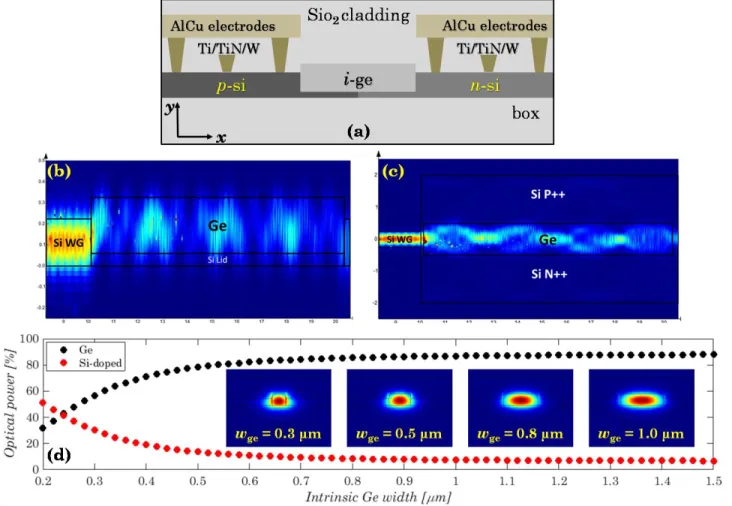
Figure 1. (a) Cross-sectional schematics (x-y plane) of the waveguide-integrated photodetector with a lateral Si-Ge-Si heterojunction. Color maps of the optical intensity distribution in the butt-waveguide-coupled pin photodetector, as simulated by 3-D FDTD tool: (b) side (y-z plane) and (c) top (x-z plane) views. (d) Evolution of the optical power confinement inside the Ge region and Si-doped lateral slabs as a function of the intrinsic Ge width. Insets: Electric field profiles of the fundamental TE-polarized waveguide mode for different widths of the Ge zone.
In this work, we present the design, fabrication, and characterization of Ge-based waveguide-integrated photodetectors that benefit from lateral Silicon-Germanium-Silicon (Si-Ge-Si) hetero-structured pin junctions31,32. Such a photodetector arrangement takes advantage of enhanced optical mode confinement in the Ge layer. This is due to the large refractive index contrast between the doped side slabs and the intrinsic Ge zone, which, in turn, reduces optical losses in the Si-doped contacts. This yields (i) additional degrees of freedom for the photodetector geometry and (ii) responsivity and bandwidth improvements. Si-Ge-Si photodetectors with a simpler and complementary
metal-oxide-semiconductor-compatible (CMOS-metal-oxide-semiconductor-compatible) fabrication scheme indeed have considerably improved performances. More specifically, a device responsivity up to 1.2 A/W, dark-currents below 150 nA, and fast device response beyond 50 GHz were demonstrated under low-reverse-bias states. In addition, a superior high-speed signal detection up to 40 Gbps was readily achieved for different types of devices, as confirmed by detailed eye diagram inspections. In addition, it is worthwhile to note that photodetector integration strategy delivers substantial technological advantages such as a decrease in contact access resistance and improvements in opto-electronics device integration, enabling fabrication later on of hybrid nanophotonic components, as flat surfaces are still present after photodetector fabrication.
2. WAVEGUIDE PHOTODETECTOR DESIGN AND FABRICATION
Figure 1(a) shows a cross-sectional schematics of the waveguide-coupled pin photodetector with a lateral Silicon-Germanium-Silicon (Si-Ge-Si) heterojunction. Photodetectors are implemented on top of silicon-on-insulator (SOI) substrates with 220-nm-thick Silicon (Si) overlayers and 2-µm-thick buried oxides (BOX). Devices are optimized for a transverse electrical (TE) polarization and operation at the C-band close to a 1.55 µm wavelength. The intrinsic Germanium (Ge) zone is sandwiched between p-type and n-type Si slabs, situated within a cavity at the end of Si waveguide. Figures 1(b) and (c) show optical intensity distribution in the butt-waveguide-coupled pin photodetector. The optical power is efficiently coupled from the single-mode injection waveguide into the intrinsic Ge zone. Simulations have been carried out using three-dimensional (3-D) Finite Difference Time Domain (FDTD) tool33 available from Lumerical Solution, Inc. for a 1-µm-wide and 10-µm-long device.
The major portion of the optical power needs to be confined within the intrinsic Ge zone in order to avoid excessive light absorption in thep-type and n-type Si contacts. The evolution of the optical power confinement as a function of the Ge zone width in the intrinsic Ge region and in the Si-doped regions is shown in Fig. 1(d). For the smallest device configuration (0.3-µm-wide Ge region), the optical power is already well-confined within the intrinsic Ge area, with a value close to 55%, while the optical power inside the lateral Si-doped regions reaches 32%. When the widthof the intrinsic Ge region increases, the optical power confinement is enhanced, with more than 80% of the power in Ge and less than 10% in the lossy Si contacts for photodetector widths higher than 0.6 µm. For a device with 1-µm-wide Ge region, i.e. the largest device configuration investigated here, the optical power in the Ge area reaches 87%. Only 8% of the optical power is then present within the doped Si slabs. Insets of Fig. 2(d) depict electric field profiles of the fundamental TE-polarized waveguide mode for different widths of the intrinsic Ge zone.
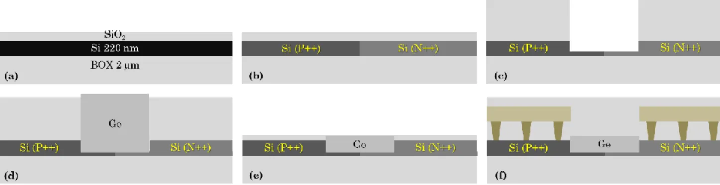
Figure2. Schematics of the process flow used to fabricate butt-waveguide-coupled photodetectors with lateral Si-Ge-Si heterojunctions. (a) Starting SOI substrate after passive device definition and thermal oxidation. (b) Ion implantations in Si layer for photodetector contact definition. (c) Etching of the Si cavity prior to selective epitaxial growth of Ge. (d) Overflowing Ge after epitaxy and annealing. (e) Photodetector after CMP. (f) Final photodetector with W plugs and AlCu electrodes.
The waveguide-integrated pin photodetectors were fabricated in CEA LETI's facilities using 200 mm SOI wafers. The SOI substrates consisted in 220-nm-thick Si films on to of 2-µm-thick BOX. Fabrication process flow for pin waveguide-coupled photodetectors is schematically illustrated in Fig. 2. At the beginning, passive nanophotonic devices, including interconnecting waveguides and surface grating couplers, were fabricated using 193-nm deep-ultraviolet (deep-UV) lithography and dry etching. A thermal oxidation of about ~10 nm was used in order to have a cap layer prior to ion implantation [see Fig. 2(a)]. Si p-type and p-type regions were obtained by ion implantation of Boron (B) and Phosphorous (P), respectively [Fig. 2(b)]. Dopant concentrations in p-type and n-type regions were over 1019
at/cm3.A 800-nm oxide layer was deposited prior to cavity patterning for the selective epitaxial growth of Ge. The upper oxide layer was fully etched down to the Si surface. The Si cavity was then etched, with around ~60 nm of Si remaining at the bottom of the cavity [Fig. 2(c)]. Then, a more than 1-µm-thick Ge layer was selectively grown inside cavities, using GeH4 and a Low Temperature / High Temperature approach in a Reduced Pressure - Chemical Vapor Deposition
(RP-CVD) chamber, followed by one hour of H2annealing at 750°C to reduce defects density [Fig. 2(d)]. The process
used resulted in the selective epitaxial growth of Ge in cavities as small as 300 nm x 5 μm. Chemical Mechanical Polishing (CMP) was used to reduce the thickness of Ge layer down to ~260-nm and recover a flat surface prior to contact and metallization steps [Fig. 2(e)]. A thick oxide layer was then deposited for Ge passivation and insulation. 400 nm x 400 nm vias were subsequently patterned and etched down to the Si doped regions. In order to improve contact resistance, silicidation was performed. Ti/TiN/W stacks were used as metal plugs. The electrodes consisted in patterned AlCu layers. A schematics of the waveguide Si-Ge-Si photodiode is provided in Fig. 2(f).
It is worth mentioning that the use of a butt-coupling approach combined with lateral pin junction arrangement enables to contact the photodetector width asingle-etch step for p-type and n-type doped regions. It otherwise offers enhanced optical performances in terms of responsivity and spectral bandwidth, as discussed in Section 3 later on. Using Si slabs to contact the photodetectorenables to get rid of at least 7 fabrication steps (compared to Ge homojunction photodetectors) in optical interconnect process flow. This includes photolithography steps, specific p-type and n-type ion implantation steps, stripping on Ge p-type and n-type doped regions, as well as an electrical activation annealing step. The same masking / ions implantation / stripping / annealing steps are indeed used for the fabrication of the Si-based optical modulators and the processing of the Si parts of our Si-Ge-Si photodetectors.
Compared tohomo-junction device architectures, the intrinsic width of the Ge waveguide photodetector is solely defined by the width of the cavity. The use of lateral Si-Ge-Si heterojunction yields a better optical confinement of the guided mode in the Ge layer compared to full Ge integration schemes15-25, since the doped regions are made of Si on each side of the Ge region. These regions have a refractive index close to that of Si, which is lower than the refractive index of Ge. Indeed, due to the improved refractive index difference between lateral Si slabs and the intrinsic Ge zone, the incoming light coupled from the Si waveguide into the Ge region, stays confined within this area and does not spread out in the Si-doped regions. As a consequence,this avoids any deleterious absorption of photo-generated carriers in the later. This new integration scheme has important advantages. It reduces the optical loss in doped contacts, allows a better control of the photodiode geometry (intrinsic width), and provides an improvement of the device performance.
3. PHOTODETECTORS CHARACTERIZATION AND EXPERIMENTAL RESULTS
We have carried out static optical measurements, small-signal radio-frequency measurements, as well as large-signal data transmission assessments in order to quantify the benefits of using Si-Ge-Si photodetectors.
3.1 Current-voltage measurements
Typical current-voltage (I-V) characterizations were performed on butt-waveguide-coupled photodetectors with hetero-structured Si-Ge-Si junctions. Under light illumination, a photo-current was generated by the device. Light coming from the tunable laser source was coupled via standard single-mode optical fiber (SMF-28) into the Si chip using surface grating couplers. The grating couplers were optimized for the TE polarization and a central wavelength of 1.55 μm.
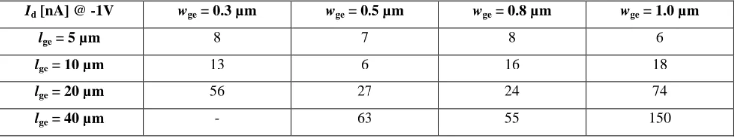
Table 1. Measured leakage dark-currents for various widths and lengths of the pin waveguide photodetectors under -1V bias. Id [nA] @ -1V wge = 0.3 µm wge = 0.5 µm wge = 0.8 µm wge = 1.0 µm
lge = 5 µm 8 7 8 6
lge = 10 µm 13 6 16 18
lge = 20 µm 56 27 24 74
Measured leakage dark-currents under -1V bias for all types of pin waveguide photodetectors are provided in Table 1. Conventional current-voltage (I-V) curves of the leakage dark-current and generated photo-current for the hetero-structured pin waveguide photodetectors are shown in Fig. 3(a). The device photo-responsivity as a function of the applied reverse voltage is shown in Fig. 3(b). The photodetector features a 1-µm-wide intrinsic Ge region with photodetector lengths of 5, 10, 20, and 40 µm.
Figure 3. (a) Measured static current-voltage characteristics under dark (solid lines) and illuminated states (dashed lines) of Si-Ge-Si hetero-structured pin waveguide photodetectors with 5, 10, 20, and 40 µm device lengths. (b) Si-Ge-Si
photodetector responsivity as a function of the reserve bias for different device lengths.
The measured devices exhibit very low leakage dark-currents, typically well-below 10 nA for the smallest devices under -1V bias conditions. The dark current increases monotonously with the length of the photodetector. However, the evolution of the dark-current with the width of the intrinsic Ge region is less clear. The highest dark-current of ~150 nA was measured in the widest and longest devices. In all tested devices, the value of dark-current are well-below 1 µA. This makes the investigated photodetectors suitable for use as high-speed and energy-efficient receivers. The generated photo-current was measured at a wavelength of 1.55µm, with an input optical power of around -16 dBm. The device showed a responsivity as high as 1.2 A/W under -1 V bias for the widest and the longest device (lge = 40 μm and wGe = 1
μm). The responsivities for 5-, 10-, 20-µm-long devices are 0.19, 0.47, and 0.73 A/W. It is worth noting that, in all cases, the device responsivity reaches its maximum at low bias voltage, typically below 0.5V. This is a highly desired feature in integrated waveguide photodetectors benefit from low-power consumption operation of nanophotonic receivers. The maximum responsivity is achieved at low bias condition, which clearly indicates that all photo-generated carriers have been collected. Furthermore, Si-Ge-Si hetero-structured photodetectors exhibit an ultra-high near-unity quantum efficiency up to ~95%, as achieved for the largest device configuration at a 0.5V reverse bias.
3.2 Small-signal radio-frequency measurements
Small-signal radio-frequency (RF) measurements were performed using a classical RF experimental set-up. Light was coupled into the Si waveguide with the help of surface grating couplers. The hetero-structuredSi-Ge-Si photodetectors were biased using 50 GHz probes. The generated photocurrent was measured using a Lightwave Component Analyzer (LCA), providing a frequency response in the 0.1 GHz to 50 GHz range.
Figure 4. Normalized frequency responses, as obtained from the small-signal radio-frequency measurements under 0V, 1V, 2V and 3V reverse bias. Photodetector in-plane dimensions of the intrinsic Ge region are: (a) wge = 0.3 µm and lge = 20 µm; (b) wge = 0.5 µm and lge = 40 µm; (c) wge = 0.8 µm and lge = 40 µm; (d) wge = 1.0 µm and lge = 40 µm.
Figure 4 shows frequency responses of waveguide-integrated Si-Ge-Si pin photodetectors under different reverse bias conditions (from 0V to 3V)and for various device dimensions ((a) wge = 0.3 µm and lge = 20 µm; (b) wge = 0.5 µm and lge
= 40 µm; (c) wge = 0.8 µm and lge = 40 µm; (d) wge = 1.0 µm and lge = 40 µm).Under 0V bias, the -3 dB cut-off
frequencies are relatively small, reaching a maximum of 5 GHz for the 0.3-µm-wide and 20-µm-long photodetectors and a maximum of 0.9 GHz for the 1.0-µm-wide and 40-µm-long photodetector. This behavior was consistently observed on other devices, without any dependence on the length of the intrinsic Ge zone.
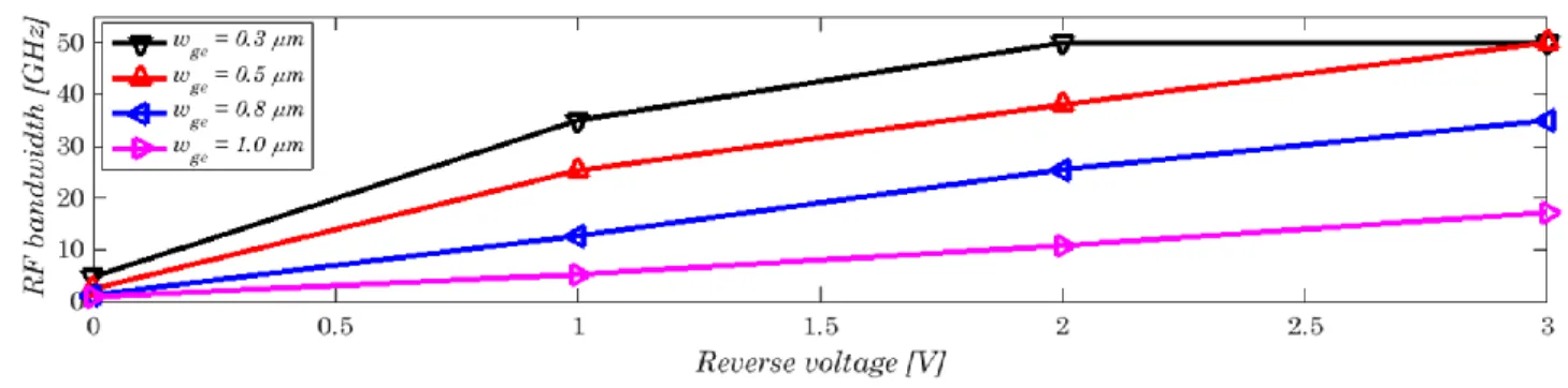
Figure 5. Summarized opto-electrical bandwidths versus reverse bias voltage for different widths of the Si-Ge-Si hetero-structured waveguide-coupled photodetectors.
Under zero bias, only the built-in electric field can extract photo-generated carriers. The wider the junction, the lower the electric field, and hence the lower the cut-off frequency is. Previous works reported23 that, for Ge pin homo-junction devices, zero-bias operation at high-speed of 40 GHz was possible. This was enabled by the single material configuration between the doped slabs and intrinsic zone, and thus the absence of electric field and band gap energy discontinuities. In pin photodetectors with hetero-structured Si-Ge-Si junctions, there are electric field discontinuities at the interfaces between the intrinsic Ge area and the lateral Si-doped slab regions. Because of that, the zero-bias bandwidth remains low in every devices. Photo-generated carriers are then unable to reach high drift velocity. This
results in a significant degradation of the zero-bias frequency response of waveguide pin photodetectors with lateral Si-Ge-Si heterojunctions.
In a stark contrast, under a reverse bias voltage of 1V, a high electric field was present in the whole Ge layer and both performance metrics, the cut-off frequency and the responsivity, definitely increased. A comprehensive summary of the extracted -3 dB cut-off frequency is provided in Figure5. For Ge photodiodes with wge= 1 μm, the bandwidth hardly
reaches 18 GHz under a high voltage, independently of the device length. This behavior is consistent with the device width, i.e. the frequency response of the device is limited by the carrier transit time.A 50 GHz bandwidth was obtained by reducing the intrinsic Ge width. In particular, this was achieved at low reverse bias voltages of 2V for wge = 0.3 μm
and 3V for wge = 0.5 μm. Another interesting feature of the studied photodetectors is that, even for the long Ge zones, the
frequency response does not seem to be limited by the RC delay. Our measurement set-up was limited to 50 GHz, whichinhibits devicecharacterizations beyond this limit.
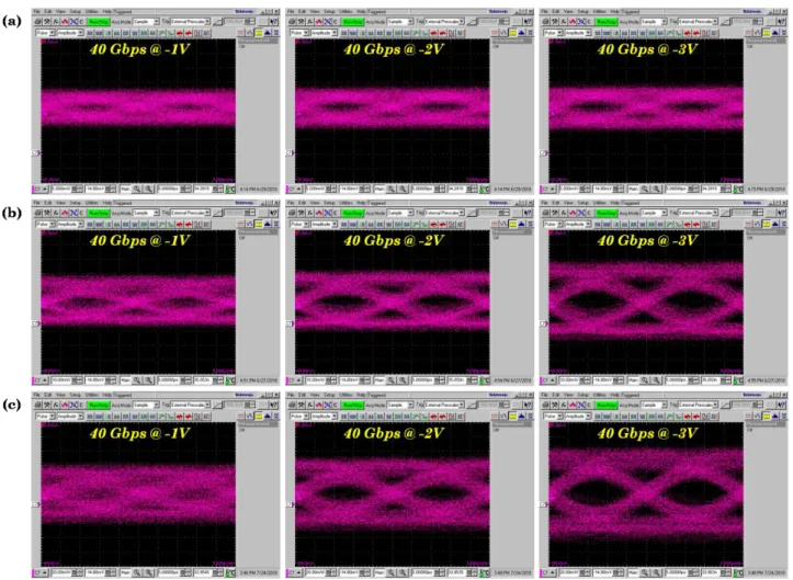
Figure 6. Evolution of eye diagram apertures under low-reverse-bias conditions at 40 Gbps transmission rate. The respective vertical scales are: (a) 5 mV/div; (b) 10 mV/div, and (c) 20 mV/div. Photodetector in-plane dimensions of the intrinsic Ge region are: (a) wge = 0.5 µm and lge = 40 µm; (b) wge = 0.8 µm and lge = 40 µm; and (c) wge = 1.0 µm and lge = 40 µm.
3.3 Large-signal data measurements
The high-speed operation of hetero-structured Si-Ge-Si pin photodetectors was further validatedvia data detection measurements. We thus performed eye-diagram large-signal acquisitions. Data weretransmitted in non-return-to-zero (NRZ) optical modulation format. The pseudo-random-binary-sequence (PRBS) data pattern of word length 27-1was consideredup to 40 Gbps data rate. The externally modulated laser generated a signal, which was amplified by an Erbium-doped fiber amplifier (EDFA), followed by an optical filter to reduce spontaneous emission noise. The optical power was controlled with a variable optical attenuator and an in-line power-meter. Optical TE polarization was adjusted with apolarization controller to optimize the power level intensity of the detected signal. The
modulated signal was sent into the Si chip thanks to a surface grating coupler, followed by on-chip detection inhetero-structured Si-Ge-Si pin photodetector. Electrical data were retrieved through the RF set-up previously employed for small-signal RFtesting, by applying the reverse voltage to the photodetector with the help of a RF probe connected to a bias-tee. Dataweredirectly sentfrom the RF bias-tee output toa high-speed sampling oscilloscope, yieldingeye diagrams without the use of an external electrical amplifier. The measured eye diagrams under different low-reverse-bias conditions and a data rate of 40 Gbps is shown in Fig. 6. Large-signal data assessmentswere carried out on devices with a 40-µm-long and 0.5-, 0.8-, and 1.0-µm-wide Ge regions.
As seen in Fig. 6, opened eye diagram apertures suggest that high-speed signal detection up to 40 Gbps is readily achieved in all studied photodetector arrangements. The limited opto-electrical bandwidth of the hetero-structured Si-Ge-Si photodetectors at 1V reverse bias explains why retrieved eye diagrams are closing. This effect is more obvious for devices with a wider intrinsic Ge region. This trend is in a good agreement with the afore-described small-signal radio-frequency measurements. Nevertheless, it is worth mentioning that the voltage control possibility preserves a superior high-data-rate detection capability, which in turn, still enables a device operation under low-reverse-voltage states.
4. CONCLUSIONS
To sum up, we experimentally showed the superior high-speed performances of advanced waveguide-integrated photodetectors with lateral Si-Ge-Si heterojunctions, this for low-reverse-voltage operation within the C-band wavelengths. The hetero-structured photodetector architecture takes full advantage of a butt-waveguide-coupled integration scheme, together with a silicon-contacted pin junction arrangement.We successfully obtained a set of integrated photodetectors with a reduced and fully CMOS-compatible fabrication complexity and considerably improved performances. A device responsivity up to 1.2 A/W, dark-currents below ~150 nA, and fast device response beyond 50 GHz were indeed achieved under low-reverse-bias conditions. In addition, a superior high-speed signal detection up to 40 Gbps was readily achieved for different types of device dimensions, as confirmed by detailed eye diagram inspections. This achievements open up a promising route towards advanced integration schemes for low-cost photo-detection, which are particularly attractive for the fabrication of nanophotonic transceivers on mature SOI substrates.
ACKNOWLEDGEMENTS
This work has received the funding from the European Research Council (ERC) under the European Union’s Horizon 2020 Research and Innovation Program (ERC POPSTAR – grant agreement No 647342).
REFERENCES
[1] L. Vivien and L. Pavesi, Handbook of Silicon Photonics (CRC Press, 2013).
[2] D. Thomson, A. Zilkie, J. E. Bowers, T. Komljenovic, G. T. Reed, L. Vivien, D. Marris-Morini, E. Cassan, L. Virot, J.-M. Fédéli, J.-M. Hartmann, J. H. Schmid, D.-X. Xu, F. Boeuf, P. O’Brien, G. Z. Mashanovich, and M. Nedeljkovic, “Roadmap on silicon photonics,” Journal of Optics 18, 073003 (2016).
[3] X. Chen, M. M. Milosevic, S. Stankovic, S. Reynolds, T. Dominguez-Bucio, K. Li, D. J. Thomson, F. Gardes, and G. T. Reed, “The Emergence of Silicon Photonics as a Flexible Technology Platform,” Proceedings of the IEEE106, 2101-2116 (2018).
[4] R. Halir, A. Ortega-Moñux, D. Benedikovic, G. Z. Mashanovich, J. G. Wangüemert-Pérez, J. H. Schmid, Í. Molina-Fernández, and P. Cheben, “Subwavelength-Grating Metamaterial Structures for Silicon Photonic Devices,” Proceedings of the IEEE106, 2144-2157 (2018).
[5] J. Chilles and S. Fathpour, “Silicon photonics beyond silicon-on-insulator,” Journal of Optics 19, 053001 (2017). [6] D. Marris-Morini, V. Vakarin, J. M. Ramirez, Q. Liu, A. Ballabio, J. Frigerio, M. Montesinos, C. Alonso-Ramos, X.
Le Roux, S. Serna, D. Benedikovic, D. Chrastina, L. Vivien, and G. Isella, “Germanium-based integrated photonics from near- to mid-infrared applications,” Nanophotonics 7, 1781-1793 (2018).
[7] M. Asghari and A. V. Krishnamoorthy, “Energy-efficient communication,” Nature Photonics 5, 268-270 (2011). [8] R. E. Camacho-Aguillera, Y. Cai, N. Patel, J. T. Bessette, M. Romagnoli, L. C. Kimerling, and J. Michel, “An
[9] A. H. Atabaki, S. Moazeni, F. Pavanello, H. Gevorgyan, J. Notaros, L. Alloatti, M. T. Wade, C. Sun, S. A. Kruger, H. Meng, K. Al Qubaisi, I. Wang, B. Zhang, A. Khilo, C. V. Baiocco, M. A. Popović, V. M. Stojanović, and R. J. Ram, “Integrating photonics with silicon nanoelectronics for the next generation of systems on a chip,” Nature 556, 349-354 (2018).
[10] G. T. Reed, G. Mashanovich, F. Y. Gardes, and D. J. Thomson, “Silicon optical modulators,” Nature Photonics 4, 518-526 (2010).
[11] D. Marris-Morini, L. Virot, C. Baudot, J.-M. Fédéli, G. Rasigade, D. Pérez-Galacho, J.-M. Hartmann, S. Oliver, P. Brindel, P. Crozat, F. Boeuf, and L. Vivien, “A 40 Gbit/s optical link on a 300-mm silicon platform,” Optics Express 22, 6674-6679 (2014).
[12] S. Fama, L. Colace, G. Masini, G. Assanto, and H.-C. Luan, “High performance germanium-on-silicon detectors for optical communications,” Applied Physics Letters 81, 586-588 (2002).
[13] S. J. Koester, J. D. Schaub, G. Delinger, and J. O. Chu, “Germanium-on-SOI infrared detectors for integrated photonic applications,” IEEE Journal of Selected Topic in Quantum Electronics 12, 1489-1502 (2006).
[14] J. Michel, J. Liu, and L. C. Kimerling, “High-performance Ge-on-Si photodetectors,” Nature Photonics 4, 527-534 (2010).
[15] L. Colace and G. Assanto, “Germanium on silicon for near-infrared light sensing,” IEEE Photonics Journal 1, 69-79 (2009).
[16] T. Yin, R. Cohen, M. M. Morse, G. Sarid, Y. Chetrit, D. Rubin, and M. J. Paniccia, “31 GHz Ge n-i-p waveguide photodetectors on Silicon-on-Insulator substrate,” Optics Express 15, 13965-13971 (2007).
[17] L. Vivien, J. Osmond, J.-M. Fédéli, D. Marris-Morini, P. Crozat, J. F. Damlencourt, E. Cassan, Y. Lecunff, and S. Laval, “42 GHz p.i.n germanium photodetector integrated in a silicon-on-insulator waveguide,” Optics Express 17, 6252-6257 (2009).
[18] D. Feng, S. Liao, P. Dong, N. Feng, N. Feng, H. Liang, D. Zheng, C. Kung, J. Fong, R. Shafilha, J. Cunningham, A. Krishnamoorthy, and M. Asghari, “High-speed Ge photodetector monolithically integrated with large cross-section silicon-on-insulator waveguide,” Applied Physics Letters 95, 261105 (2009).
[19] J. Joo, S. Kim, I. G. Kim, K.-S. Jang, and G. Kim, “High-sensitivity 10 Gbps Ge-on-Si photoreceiver operating at λ~1.55 µm,” Optics Express 18, 16474-16479 (2010).
[20] S. Assefa, F. Xia, S. W. Bedell, Y. Zhang, T. Topuria, P. M. Rice, and Y. A. Vlasov, “CMOS-integrated high-speed MSM germanium waveguide photodetector,” Optics Express 18, 4986-4999 (2010).
[21] S. Liao, N.-N. Feng, D. Feng, P. Dong, R. Shafilha, C.-C. Kung, H. Liang, W. Qian, Y. Liu, J. Fong, J. E. Cunningham, Y. Luo, and M. Asghari, “36 GHz submicron silicon waveguide germanium photodetector,” Optics Express 19, 10967-10972 (2011).
[22] C. T. DeRose, D. C. Trotter, W. A. Zortman, A. L. Starbuck, M. Fisher, M. R. Watts, and P. S. Davids, “Ultra compact 45 GHz CMOS compatible Germanium waveguide photodiode with low dark current,” Optics Express 19, 24897-24904 (2011).
[23] L. Vivien, A. Polzer, D. Marris-Morini, J. Osmond, J. M. Hartman, P. Crozat, E. Cassan, C. Kopp, H. Zimmermann, and J.-M. Fédéli, “Zero-bias 40 Gbit/s germanium waveguide photodetector on silicon,” Optics Express 20, 1096-1101 (2012).
[24] G. Li, Y. Luo, X. Zheng, G. Masini, A. Mekis, S. Sahni, H. Thacker, J. Yao, I. Shubin, K. Raj, J. E. Cunningham, and A. V. Krishnamoorthy, “Improving CMOS-compatible Germanium photodetectors,” Optics Express 20, 26345-26350 (2012).
[25] H. Pan, S. Assefa, W. M. J. Green, D. M. Kuchta, C. L. Schow, A. V. Rylyakov, B. G. Lee, C. W. Baks, S. M. Shank, and Y. A. Vlasov, “High-speed receiver based on waveguide germanium photodetector wire-bonded to 90nm SOI CMOS amplifier,” Optics Express 20, 18145-18155 (2012).
[26] L. Virot, L. Vivien, J.-M. Fédéli, Y. Bogumilowitz, J.-M. Hartmann, F. Boeuf, P. Crozat, D. Marris-Morini, and E. Cassan, “High-performance waveguide-integrated germanium PIN photodiodes for optical communication applications,” Photonics Research 1, 140-147 (2013).
[27] Y. Zhang, S. Yang, Y. Yang, M. Gould, N. Ophir, A. E.-J. Lim, G.-Q. Lo, Y P. Magill, K. Bergman, T. Baehr-Jones, Y and M. Hochberg, “A high-responsivity photodetector absent metal-germanium direct contact,” Optics Express 22, 11367-11375 (2014).
[28] H. T. Chen, P. Verheyen, P. De Heyn, G. Lepage, J. De Coster, P. Absil, G. Roelkens, and J. Van Campenhout, “High-responsivity low-voltage 28-Gb/s Ge p-i-n photodetector with silicon contacts,” IEEE Journal of Lightwave Technology 33, 820-824 (2015).
[29] H. Chen, P. Verheyen, P. De Heyn, G. Lepage, J. De Coster, S. Balakrishnan, P. Absil, W. Yao, L. Shen, G. Roelkens, and J. Van Campenhout, “-1 V 67 GHz bandwidth Si-contacted germanium waveguide p-i-n photodetector for optical links at 56 Gbps and beyond,” Optics Express 24, 4622-4631 (2016).
[30] H. Chen, P. Verheyen, P. De Heyn, G. Lepage, J. De Coster, S. Balakrishnan, P. Absil, G. Roelkens, and J. Van Campenhout, “Dark current analysis in high-speed germanium p-i-n waveguide photodetectors,” Journal of Applied Physics19, 213105 (2016).
[31] L. Virot, D. Benedikovic, B. Szelag, C. Alonso-Ramos, B. Karakus, J.-M. Hartmann, X. Le Roux, P. Crozat, E. Cassan, D. Marris-Morini, Ch. Baudot, F. Boeuf, J.-M. Fédéli, C. Kopp, and L. Vivien, “Integrated waveguide PIN photodiodes exploiting lateral Si/Ge/Si heterojunction,” Optics Express 16, 19487-19496 (2017).
[32] D. Benedikovic, L. Virot, G. Aubin, F. Amar, B. Szelag, B. Karakus, J.-M. Hartmann, C. Alonso-Ramos, X. Le Roux, P. Crozat, E. Cassan, D. Marris-Morini, C. Baudot, F. Boeuf, J.-M. Fédéli, C. Kopp, and L. Vivien, “25 Gbps low-voltage hetero-structured silicon-germanium waveguide pin photodetectors for monolithic on-chip nanophotonic architectures,” Photonics Research(under review),November 2018.