Gain characterization and passive modelocking
of electrically pumped VECSELs
W.P. Pallmann,1,* C.A. Zaugg,1 M. Mangold,1 V.J. Wittwer,1 H. Moench,2 S. Gronenborn,2 M. Miller,3 B.W. Tilma,1 T. Südmeyer,1 and U. Keller1 1Department of Physics, Institute for Quantum Electronics, ETH Zurich, 8093 Zurich, Switzerland 2Philips Technologie GmbH Innovative Technologies, Weisshausstrasse 2, 52066 Aachen, Germany
3Philips Technologie GmbH U-L-M Photonics, Lise-Meitner-Strasse 13, 89081 Ulm, Germany *pallmann@phys.ethz.ch
Abstract: Linear and nonlinear gain characterization of electrically pumped
vertical external cavity surface emitting lasers (EP-VECSELs) is presented with spectrally resolved measurements of the gain and with gain saturation measurements of two EP-VECSEL samples with different field enhancement in the quantum-well gain layers. The spectral bandwidth, small-signal gain and saturation fluence of the devices are compared. Using the sample with the larger bandwidth, we have demonstrated the shortest pulses generated from a passively modelocked EP-VECSEL to date. With a low-saturation-fluence SESAM for passive modelocking we have achieved 9.5-ps pulses with 7.6 mW average output power at a repetition rate of 1.4 GHz. With a higher output coupler transmission the pulse duration was increased to 31 ps with an average output power of 13.6 mW. The pulses were chirped mainly due to the group delay dispersion (GDD) introduced by the intermediate DBR, which compensates the optical loss in the structure.
OCIS codes: (140.5960) Semiconductor lasers; (140.7270) Vertical emitting lasers; (140.4050)
Mode-locked lasers.
References and links
1. M. Kuznetsov, F. Hakimi, R. Sprague, and A. Mooradian, “High-power (>0.5-W cw) diode-pumped vertical-external-cavity surface-emitting semiconductor lasers with circular TEM00 beams,” IEEE Photon. Technol. Lett.
9(8), 1063–1065 (1997).
2. U. Keller, “Recent developments in compact ultrafast lasers,” Nature 424(6950), 831–838 (2003).
3. U. Keller, K. J. Weingarten, F. X. Kärtner, D. Kopf, B. Braun, I. D. Jung, R. Fluck, C. Hönninger, N. Matuschek, and J. Aus der Au, “Semiconductor saturable absorber mirrors (SESAMs) for femtosecond to nanosecond pulse generation in solid-state lasers,” IEEE J. Sel. Top. Quantum Electron. 2(3), 435–453 (1996).
4. U. Keller and A. C. Tropper, “Passively modelocked surface-emitting semiconductor lasers,” Phys. Rep. 429(2), 67–120 (2006).
5. A. H. Quarterman, K. G. Wilcox, V. Apostolopoulos, Z. Mihoubi, S. P. Elsmere, I. Farrer, D. A. Ritchie, and A. Tropper, “A passively mode-locked external-cavity semiconductor laser emitting 60-fs pulses,” Nat. Photonics
3(12), 729–731 (2009).
6. P. Klopp, U. Griebner, M. Zorn, and M. Weyers, “Pulse repetition rate up to 92 GHz or pulse duration shorter than 110 fs from a mode-locked semiconductor disk laser,” Appl. Phys. Lett. 98(7), 071103 (2011). 7. M. Hoffmann, O. D. Sieber, V. J. Wittwer, I. L. Krestnikov, D. A. Livshits, Y. Barbarin, T. Südmeyer, and U.
Keller, “Femtosecond high-power quantum dot vertical external cavity surface emitting laser,” Opt. Express
19(9), 8108–8116 (2011).
8. M. Scheller, T. L. Wang, B. Kunert, W. Stolz, S. W. Koch, and J. V. Moloney, “Passively modelocked VECSEL emitting 682 fs pulses with 5.1W of average output power,” Electron. Lett. 48(10), 588–589 (2012).
9. U. Keller, “Ultrafast solid-state laser oscillators: a success story for the last 20 years with no end in sight,” Appl. Phys. B 100(1), 15–28 (2010).
10. V. J. Wittwer, C. A. Zaugg, W. P. Pallmann, A. E. H. Oehler, B. Rudin, M. Hoffmann, M. Golling, Y. Barbarin, T. Sudmeyer, and U. Keller, “Timing jitter characterization of a free-running SESAM mode-locked VECSEL,” IEEE Photon. J. 3(4), 658–664 (2011).
11. D. J. H. C. Maas, A.-R. Bellancourt, B. Rudin, M. Golling, H. J. Unold, T. Südmeyer, and U. Keller, “Vertical integration of ultrafast semiconductor lasers,” Appl. Phys. B 88(4), 493–497 (2007).
12. B. Rudin, V. J. Wittwer, D. J. H. C. Maas, M. Hoffmann, O. D. Sieber, Y. Barbarin, M. Golling, T. Südmeyer, and U. Keller, “High-power MIXSEL: an integrated ultrafast semiconductor laser with 6.4 W average power,” Opt. Express 18(26), 27582–27588 (2010).
13. Y. Barbarin, M. Hoffmann, W. P. Pallmann, I. Dahhan, P. Kreuter, M. Miller, J. Baier, H. Moench, M. Golling, T. Südmeyer, B. Witzigmann, and U. Keller, “Electrically pumped vertical external cavity surface emitting lasers suitable for passive modelocking,” IEEE J. Sel. Top. Quantum Electron. 17(6), 1779–1786 (2011).
14. J. G. McInerney, A. Mooradian, A. Lewis, A. V. Shchegrov, E. M. Strzelecka, D. Lee, J. P. Watson, M. Liebman, G. P. Carey, B. D. Cantos, W. R. Hitchens, and D. Heald, “High-power surface emitting semiconductor laser with extended vertical compound cavity,” Electron. Lett. 39(6), 523–525 (2003). 15. K. Jasim, Q. Zhang, A. V. Nurmikko, A. Mooradian, G. Carey, W. Ha, and E. Ippen, “Passively modelocked
vertical extended cavity surface emitting diode laser,” Electron. Lett. 39(4), 373–375 (2003).
16. K. Jasim, Q. Zhang, A. V. Nurmikko, E. Ippen, A. Mooradian, G. Carey, and W. Ha, “Picosecond pulse generation from passively modelocked vertical cavity diode laser at up to 15 GHz pulse repetition rate,” Electron. Lett. 40(1), 34–35 (2004).
17. R. Paschotta, R. Häring, U. Keller, A. Garnache, S. Hoogland, and A. C. Tropper, “Soliton-like pulse-shaping mechanism in passively mode-locked surface-emitting semiconductor lasers,” Appl. Phys. B 75(4-5), 445–451 (2002).
18. M. Hoffmann, O. D. Sieber, D. J. H. C. Maas, V. J. Wittwer, M. Golling, T. Südmeyer, and U. Keller,
“Experimental verification of soliton-like pulse-shaping mechanisms in passively mode-locked VECSELs,” Opt. Express 18(10), 10143–10153 (2010).
19. M. Mangold, V. J. Wittwer, O. D. Sieber, M. Hoffmann, I. L. Krestnikov, D. A. Livshits, M. Golling, T. Südmeyer, and U. Keller, “VECSEL gain characterization,” Opt. Express 20(4), 4136–4148 (2012). 20. P. Kreuter, B. Witzigmann, D. J. H. C. Maas, Y. Barbarin, T. Südmeyer, and U. Keller, “On the design of
electrically-pumped vertical-external-cavity surface-emitting lasers,” Appl. Phys. B 91(2), 257–264 (2008). 21. J. G. McInerney, A. Mooradian, A. Lewis, A. V. Shchegrov, E. M. Strzelecka, D. Lee, J. P. Watson, M. K.
Liebman, G. P. Carey, A. Umbrasas, C. A. Amsden, B. D. Cantos, W. R. Hitchens, D. L. Heald, V. V. Doan, and J. L. Cannon, “Novel 980-nm and 490-nm light sources using vertical cavity lasers with extended coupled cavities,”in SPIE 2003, (SPIE, 2003), 21–31.
22. J. R. Orchard, D. T. D. Childs, L. C. Lin, B. J. Stevens, D. M. Williams, and R. Hogg, “Tradeoffs in the realization of electrically pumped vertical external cavity surface emitting lasers,” IEEE J. Sel. Top. Quantum Electron. 17(6), 1745–1752 (2011).
23. M. Haiml, R. Grange, and U. Keller, “Optical characterization of semiconductor saturable absorbers,” Appl. Phys. B 79(3), 331–339 (2004).
24. L. M. Frantz and J. S. Nodvik, “Theory of pulse propagation in a laser amplifier,” J. Appl. Phys. 34(8), 2346– 2349 (1963).
25. U. Keller, “Ultrafast solid-state lasers,” in Landolt-Börnstein. Laser Physics and Applications. Subvolume B:
Laser Systems. Part I., G. Herziger, H. Weber, and R. Proprawe, eds. (Springer Verlag, 2007), pp. 33–167.
26. G. J. Spühler, K. J. Weingarten, R. Grange, L. Krainer, M. Haiml, V. Liverini, M. Golling, S. Schon, and U. Keller, “Semiconductor saturable absorber mirror structures with low saturation fluence,” Appl. Phys. B 81(1), 27–32 (2005).
27. D. J. H. C. Maas, B. Rudin, A.-R. Bellancourt, D. Iwaniuk, S. V. Marchese, T. Südmeyer, and U. Keller, “High precision optical characterization of semiconductor saturable absorber mirrors,” Opt. Express 16(10), 7571–7579 (2008).
1. Introduction
Optically-pumped vertical external cavity surface emitting lasers (OP-VECSELs) [1] can offer several watts of average output power in circular, diffraction-limited beams. Their external cavity geometry enables passive modelocking with a semiconductor saturable absorber mirror (SESAM [2, 3]). Such passively modelocked ultrafast VECSELs [4] have generated sub-100-fs pulses in bursts of pulses [5], 107-fs pulses in fundamental modelocking at moderate output powers [6] and multi-Watt average output power with longer pulses around 700 fs to 800 fs [7, 8]. These OP-VECSELs, similar to SESAM modelocked solid-state lasers [9], provide excellent noise properties [10], but additionally offer more flexibility in the emission wavelength. In addition, using a semiconductor gain material allows for more compact cavity designs, which would make them highly attractive for many industrial and commercial applications. One advantage is the possibility to integrate the absorber directly into the semiconductor gain structure, referred to as the MIXSEL (modelocked integrated external cavity surface emitting laser) concept [11]. With an optically pumped MIXSEL we have demonstrated 6.4 W of average output power in 28.1 ps pulses [12]. Another advantage is the possibility for electrical pumping.
For a SESAM modelocked electrically pumped VECSEL (EP-VECSEL) it is necessary to obtain stable transverse mode operation. Fundamental Gaussian mode operation requires a
more careful design because of the many different tradeoffs between optimized optical and electrical properties [13]. Most importantly, a high modal gain is required to overcome optical loss introduced by free carrier absorption. This loss mainly originates from the doping necessary to reduce electrical resistance. The high optical gain is typically obtained with a resonant design, i.e. a strong enhancement of the optical field at the position of the gain quantum-wells. The trade-offs for modelocking are increased group delay dispersion (GDD) and a decreased gain bandwidth, setting a lower limit for the pulse duration.
In 2003, the Novalux corporation demonstrated a continuous-wave (cw) output power of 500 mW in a TEM00 mode with their proprietary EP-VECSEL design, referred to as the
NECSEL [14]. Despite the impressive cw performance of these devices, modelocking results have been limited to 40 mW of average output power with 57-ps pulses [15] and some tens of milliwatts with 15-ps pulses [16].
In 2011, we discussed optimized design guidelines for ultrafast EP-VECSELs and emphasized the trade-off between output power and beam quality. We demonstrated that a large field enhancement starts to limit the mode quality at higher output powers. We not only measured the current injection profiles of EP-VECSEL devices with different bottom contact size, but also explained them with theoretical models for the first time [13]. Here in this paper we discuss the influence of the field enhancement on the gain to optimize the modelocking performance towards shorter pulse durations and higher output powers. Especially the strong gain saturation needs to be investigated in detail as the pulse formation mechanism in a SESAM-modelocked VECSEL is governed by strong dynamic gain and absorber saturation [17, 18]. Therefore, we present the first detailed measurement of emission bandwidth, small-signal gain and gain saturation of EP-VECSELs as function of field enhancement. We used two high-precision reflectivity measurement setups as described in [19]. The EP-VECSEL structure with lower field enhancement provides a gain bandwidth of more than 3 nm at moderate saturation fluences of 6.2 μJ/cm2 and was SESAM modelocked to generate pulses
with 9.5 ps FWHM duration at an average power of 7.6 mW and a pulse repetition rate of 1.4 GHz. This has been the shortest pulse duration generated from a modelocked EP-VECSEL to date. Issues and challenges for further power scaling are discussed as well.
2. EP-VECSEL gain structure
In this first section we describe the basic design of the EP-VECSEL structures and compare their cw lasing and their electrical performance. The characterized EP-VECSELs were manufactured by Philips.
2.1 Basic design
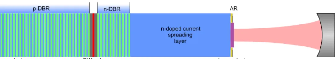
Figure 1 shows a schematic of a typical EP-VECSEL. Current is injected into the device through a disk-shaped bottom contact (140 μm in diameter) underneath the p-doped, highly reflecting distributed Bragg reflector (DBR) and through a top ring electrode (opening of 200 μm in diameter). It is assumed that the holes in the p-doped region have a lower mobility compared to the electrons in the n-doped region and remain in the center of the device above the bottom contact, whereas the highly mobile electrons move through the current spreading layer to the center of the structure with the quantum well (QW) gain layers where they recombine with the holes [20]. Thus, the current spreading layer together with the bottom disk contact helps to create a confined inversion profile to support a fundamental lasing mode. Additionally, an oxide aperture in the active region confines the current in the QWs to about 100 µm in diameter. By using this aperture a larger bottom contact can be used while maintaining the current injection profile, which slightly reduces the electrical resistance of the device.
p-DBR n-DBR QW gain AR n-doped current spreading layer OC
bottom contact top contact
Fig. 1. Schematic of an electrically pumped (EP) VECSEL gain chip with the external cavity (not to scale): Bottom disc contact and top ring electrode inject current into the structure. The p-DBR acts as end mirror for the laser wavelength. The gain section consists of several quantum wells (QWs), the partial-reflective intermediate n-DBR increases the field enhancement. The current spreading layer (CSL) supports a homogeneous current injection to the center of the device. The dielectric anti-reflection (AR) coating reduces unwanted sub-cavity effects from the CSL. A curved output coupler (OC) completes the laser sub-cavity.
The EP-VECSEL structure is entirely grown by molecular beam epitaxy (MBE). The p-doped DBR as well as the n-p-doped intermediate DBR consist of alternating λ/4-layers of Al12Ga88As and Al90Ga10As. The active region consists of three InGaAs quantum-wells
(QWs) embedded in GaAs barriers and placed in one antinode of the standing wave pattern of the electric field. The emission wavelength of the QWs is detuned towards shorter wavelengths by 12 nm from the design wavelength of 980 nm. This was necessary to ensure matching of the cavity resonance and peak gain wavelength of the QWs at a high-power operation point, as already described in great detail in [21].
Compared to OP-VECSELs, an EP-VECSEL needs to be doped to increase the electrical conductivity. This leads to additional optical loss caused by free carrier absorption. Therefore an intermediate n-doped DBR is introduced to increase the field enhancement in the quantum wells and thus the gain, and to lower the field enhancement in the current spreading layer (CSL) and thus the loss. The field enhancement Γ in the gain is defined as the amplitude of the standing wave pattern at the position of the QWs normalized by the incident electric field amplitude. The right number of quarter-wave layer pairs in the intermediate n-DBR is essential for fundamental transversal mode operation at high power levels. A low number results in low field enhancement and thus low output power due to low gain, whereas a high number leads to deterioration in beam quality, as this reduces the mode control of the output coupler (OC). This tradeoff has previously been discussed in [13]. Another effect that needs to be considered here is that the resonant sub-cavity between the two DBRs leads to a spectral filter, which strongly decreases the gain bandwidth of the structure. At the same time this leads to strong oscillations of the GDD around the lasing wavelength in the order of several 10’000 fs2. The characterized devices exhibit 9 and 13 n-DBR quarter-wave layer pairs. This
corresponds to a reflectivity of 71% and 89%, respectively. The calculated field enhancement in the QWs is Γ ≈12 (9 pairs) and Γ ≈35 (13 pairs).
The current spreading layer (CSL) is realized by mechanically thinning down the low n-doped GaAs substrate. Besides the number of n-DBR pairs, the exact thickness of the remaining substrate is the only difference between the devices from the design point of view. We will show later that this thickness can be extracted from the gain spectra. The two chips exhibit a thickness of 59.8 μm (9 pairs) and 148.3 μm (13 pairs). This difference in thickness is due to an optimization in the processing scheme of the devices, the influence of the thickness has already been discussed based on numerical simulations in [20]. This means that the 13-pair device has a higher loss due to free carrier absorption. Furthermore the devices originate from different growth runs and were processed separately, potentially giving rise to additional differences in device performance.
A dielectric antireflection (AR) coating consisting of a λ/4-layer of silicon nitride is deposited on top of the structure to reduce sub-cavity effects from the remaining substrate. The structure is mounted with the p-side down on an AlN heatsink tile, which is soldered on a TO-can mount for easy electrical testing. More details on the design and fabrication of EP-VECSELs are discussed in [13, 20, 22].
2.2 Electrical and cw lasing characterization
For better comparison of the devices, their light-current-voltage (LIV) curves were measured first. Figure 2(a) compares the current-voltage curves of the two devices for two different heatsink temperatures. The device with 9 pairs shows a lower voltage drop and both devices show an increase in voltage with decreasing temperature, as one would expect from the semiconductor material.
Fig. 2. (a) IV curves of the two different devices measured at −10 °C (dashed) and 20 °C (solid). (b) Multimode LI curves at −10 °C measured in a simple straight cavity using an OC with a radius of curvature of 15 mm and a transmission depending on the field enhancement (9 pairs: 5.7%, 13 pairs: 10.6%)
The LI characteristics in Fig. 2(b) show the optical multimode cw output power of the two lasers at a heatsink temperature of −10 °C. The EP-VECSEL cavity consists of an OC with a radius of curvature of 15 mm. The optimal transmission for the highest output power depends on the field enhancement in the gain of the structure. The optimum found was 10.6% for the 13-pair device and 5.7% for the 9-pair device. As expected, the 13-pair device reaches a higher output power due to higher gain. On the other hand, the thicker current spreading layer, which introduces a higher optical loss due to free carrier absorption, limits the achievable output power. Previously, the influence of the field enhancement on the beam quality has already been investigated for these two devices [13]. The 9-pair device allowed for fundamental TEM00 mode operation, which was not the case for the more resonant 13-pair
structure. The high reflectivity of 89% of the intermediate n-DBR reduces the beam control of the OC. The best beam quality achievable for this chip was an M2 of 2.6. Higher order modes
can destabilize modelocking and thus make this device less suitable for modelocking experiments.
3. Gain characterization
To characterize the gain properties of the different devices, we have employed two different high-precision reflectivity measurement setups. One uses a wavelength-tunable cw laser for the characterization of the spectral gain and the other setup uses a modelocked picosecond probe laser to measure the gain saturation. The two measurement setups will be described briefly, a detailed description can be found in [19].
3.1 Measurement method for spectral gain characterization
The EP-VECSEL gain structure is a resonant structure and thus, dependent on the strength of the field enhancement, its gain bandwidth is limited. Furthermore, the gain spectrum of an EP-VECSEL shifts depending on the heatsink temperature and the injected electric current. To characterize the bandwidth and the wavelength of the gain, the wavelength-dependent reflectivity of a pumped EP-VECSEL gain chip is measured. For this we used a commercially
available cw Ti:Sapphire Laser (Spectra Physics 3900S) with a lasing linewidth below 0.15 nm. The output power is attenuated to 3 mW at 960 nm and drops to 2 mW at higher wavelength. For each measured data point of the gain spectrum, the emission wavelength of the laser is tuned with a birefringent filter and the absolute value of the reflectivity is determined as described in [19]. With each sample this is repeated for different injected electric currents and heatsink temperatures.
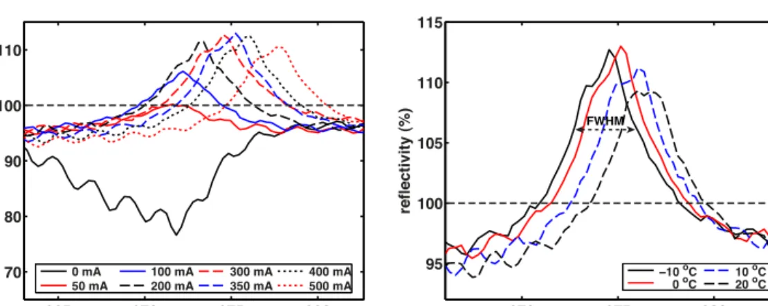
Fig. 3. Measured gain spectra for the EP-VECSEL with an intermediate n-DBR with 9 quarter-wave layer pairs (i.e. with 9 n-DBR pairs). (a) Reflectivity spectra of the EP-VECSEL for different injected electric currents at a constant heatsink temperature of −10 °C. A small-signal gain of 13% is reached at 350 mA. The modulations on the spectra arise from the current spreading layer, which acts as a weak sub-cavity because the AR-coating is not perfect. (b) Temperature dependence of the gain for an injected electric current of 300 mA. The gain bandwidth of the device is around 3.1 nm (FWHM).
3.2 Spectral gain characterization
Figure 3(a) shows the measured gain spectra of the EP-VECSEL gain chip with 9 n-DBR pairs as a function of the injected electric current. The unpumped structure (black line) shows strong absorption mainly due to the quantum-wells and the free-carrier absorption in the device. The modulations on the gain spectra originate from the current spreading layer, which acts as a Fabry-Perot-etalon and thus a spectral filter because of the residual reflection of the AR coating. The spacing of the Fabry-Perot fringes can be used to calculate the thickness of the CSL and yields a value of 59.8 μm. Increasing the injected current first results in transparency of the structure (red solid line), for higher currents gain starts to build up. The unsaturated gain is defined by a reflectivity exceeding 100%, indicated by the black dashed line. The maximum unsaturated small signal gain of 13% is reached at 350 mA. For even higher currents, a lower gain is observed, because the peak gain wavelength of the QWs shifts stronger with increased temperature than the structural resonance wavelength. This thermal wavelength shift is caused by the Joule heating associated with the electrical loss of the device. Another contribution comes from the optical loss mainly caused by free carrier absorption. Figure 3(b) shows the measured gain spectra for different heatsink temperatures and a constant injected current of 300 mA. For every current there is a temperature where the peak of the cavity resonance and the peak gain of the QWs overlap. Decreasing the temperature results in a larger detuning and thus allows for higher pump currents until this operation point is reached. For a current of 300 mA, a temperature of 0 °C is the optimum operation point for maximum gain.
The negative effect of the etalon caused by the CSL becomes evident when we compare these spectra. At a heatsink temperature of 20 °C the minimum of the modulation overlaps with the peak of the gain spectrum, reducing the maximum achievable gain. This device exhibits a gain bandwidth of about 3.1 nm and the gain peak shifts with around 13.1 nm/A
and 0.067 nm/K. This corresponds to the typical value of around 0.07 nm/K found in literature [21]. The measured values are an average over all measured spectra.
Figure 4 shows the current- and temperature-dependent gain spectra of the device with 13 n-DBR pairs. The resolution of the gain spectra is limited to 0.15 nm due to the accuracy of the feedback loop, which controls the wavelength of the probe laser. This limits the number of data points for these spectra.
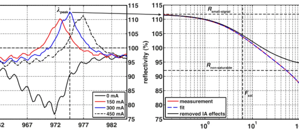
Fig. 4. Measured gain spectra for EP-VECSEL device with an intermediate n-DBR with 13 quarter-wave layer pairs (i.e. 13 n-DBR pairs). (a) Reflectivity spectra of the EP-VECSEL for different injected electric currents at a constant heatsink temperature of −10 °C. The resolution is limited by the accuracy of the feedback loop controlling the wavelength of the probe laser. A small-signal gain of 58.6% is reached at 300 mA. (b) Temperature dependence of the gain spectra for a constant injected electric current of 300 mA. The bandwidth of the structure is around 0.9 nm.
In comparison to the EP-VECSEL gain chip with 9 pairs, the maximum achievable small signal gain is significantly higher with 58.6%. On the other hand, the stronger resonance results in a much lower gain bandwidth of around 0.9 nm. The temperature-dependent measurements in Fig. 4(b) shows again the spectral filtering effect of the CSL, reducing the achievable small-signal gain at 0 °C by almost 15%. The thickness of the CSL calculated from the modulation on the spectra is 148.3 μm for this device. The structure exhibits a gain shift of around 12.8 nm/A and 0.071 nm/K.
3.3 Measurement method for gain saturation
Figure 5 shows the basic approach to determine the saturation behavior of an EP-VECSEL gain chip. First it is necessary to know the exact wavelength of the gain maximum λpeak for a
certain injected electric current and heatsink temperature. This is depicted in Fig. 5(a), using the measured gain spectra of the device with 9 n-DBR pairs at a heatsink temperature of −10 °C as an example. Then it is possible to tune a pulsed probe laser to this wavelength and to determine the reflectivity as function of fluence on the chip for this fixed wavelength. This measurement is shown in Fig. 5(b) for a wavelength of 974.4 nm for the probe laser, a heatsink temperature of −10 °C and a pump current of 300 mA. From this measurement the saturation fluence, small-signal gain, non-saturable losses and the effect of induced absorption (IA) can be extracted by fitting the data with an appropriate fit-function. The fit-function will be described later in more detail.
The laser source used for the saturation measurement is a modelocked Ti:sapphire laser (Spectra Physics Tsunami) with a pulse duration of about 1.75 ps and a spectral bandwidth of around 0.6 nm. The pulse duration is deliberately tuned to picoseconds to limit the emission bandwidth of the laser. Otherwise it would not be possible to accurately characterize the EP-VECSELs since they exhibit a narrow gain spectrum. The fluence-dependent reflectivity is measured by adjusting the power of the probe laser with a controllable attenuation stage.
Fig. 5. (a) Gain spectrum of the EP-VECSEL device with an intermediate n-DBR with 9 quarter wave layer pairs for different injected electric currents at −10 °C. The maximum gain is reached at the wavelength λpeak, to where the wavelength of the picosecond probe laser is tuned
for the measurement of the gain saturation. (b) Gain saturation measurement (red) at an injected pump current of 300 mA and −10 °C heatsink temperature. From the fit function (blue, dashed) the parameters small-signal gain reflectivity Rsmall-signal, saturation fluence Fsat, the
non-saturable reflectivity Rnon-saturable and the strength of the induced absorption F2 can be extracted.
The black curve shows the gain saturation for which the induced absorption (IA) effects were numerically removed.
For each fluence on the sample the absolute value of the reflectivity is determined using the setup described in [19]. To extract the relevant parameters from the measurement data, a fit-function based on the partial differential equation for absorber saturation in SESAMs [23] and the Frantz-Nodvik-equation for gain saturation [24] is used. Here, only the final equation of the fit-function will be given, a complete mathematical description and derivation can be found in [19, 23]. The reflectivity model function for a probe beam with a flat-top intensity profile is
[
]
FlatTop sat ss
ns
ns sat 2
( ) exp= ( ) = ln 1 exp + exp −1exp− ,
F R F F R F g F R F R F F (1.1)
where R is the reflectivity, F is the fluence on the sample and g is the gain coefficient. Even for very high fluences, the reflectivity of the unpumped device will not reach 100% due to non-saturable losses due to effects like scattering and free-carrier absorption. Rns accounts for
these non-saturable losses and is the corresponding reduced reflectivity from 100%. The saturation fluence Fsat is defined as the fluence, where the gain has dropped to approximately
(1-1/e) ≈63% of its initial value. Rsmall-signal (Rss) is the reflectivity corresponding to the
small-signal gain. The last term addresses the influence of induced absorption (IA). Especially for longer pulses, induced absorption not only occurs due to two-photon absorption but other contributions also come from free-carrier absorption or thermal effects [23]. The effect of induced absorption causes the reflectivity to drop at high fluences. It is included in the fit function in the last term, where F2 is the fluence at which the reflectivity has dropped to 1/e
≈37% because of induced absorption.
Equation (1.1) holds only for a flat-top beam. The used probe laser exhibits a Gaussian intensity distribution. For such an intensity distribution FGauss(r) = F
0 exp(−2r2/w2) the
following equation needs to be included in the fit: 1
Gauss FlatTop 0
( ) d (2 ),
R F =
zR Fz (1.2)For our EP-VECSELs some approximations for the fit function need to be re-evaluated. In the derivation of the fit function we used the approximation exp(gss) ≈1 + gss. This
approximation is still good for the device with 9 n-DBR pairs, however, slightly exceeded for the 13 pair structure, which has a small-signal gain ≈58%. Nevertheless, the parameters extracted from the fit give approximate values of how the device compares to the less resonant one.
The second approximation was made with regards to the saturable loss. This non-saturable loss is higher due to free carrier absorption in the thick CSL. We can take this into account when we introduce an effective small-signal gain
ss,eff ss (100 ns),
g =g + −R (1.3)
which accounts for the fact that these additive losses also need to be compensated before reaching the gain threshold. Then the definition of the saturation fluence Fsat mentioned above
is valid also for these devices. The small-signal gain gss is still defined as a reflectivity value
exceeding 100%.
3.4 Characterization of gain saturation
Fig. 6. Gain saturation measurement of the two devices at a heatsink temperature of −10 °C and an injected electric current of 300 mA. The measurement data (circles) is modeled to the fit function (solid line). The extracted parameters from the fit function are: Fsat: 3.2 μJ/cm2, gss:
58.3%, F2: 1.02 mJ/cm2, Rns: 69.4% for the 13 n-DBR pairs (13p) EP-VECSEL and Fsat: 6.2
μJ/cm2, g
ss: 12%, F2: 1.26 mJ/cm2, Rns: 92.25% for the 9 n-DBR pairs (9p) EP-VECSEL.
Figure 6 shows the gain saturation measurements for the two devices at a heatsink temperature of −10 °C and an injected electric pump current of 300 mA. The EP-VECSEL with 9 n-DBR pairs exhibits a saturation fluence Fsat = 6.2 μJ/cm2 and a small-signal gain gss
= 12%, the device with 13 pairs has a saturation fluence Fsat = 3.2 μJ/cm2 and a small-signal
gain gss = 58.3%. The fit function for the 13-pair device still fits the measurements data very
well, even though the approximations assumed for the fit function become less valid. Consequently, the extracted parameters should be seen only as an approximation for this device. For both measurements the small-signal gain shows excellent agreement with the value determined from the spectral gain measurements.
4. Modelocking experiments and results
The low saturation fluence combined with the limited gain bandwidth makes the EP-VECSEL device with the intermediate, 13-pair n-DBR less attractive for modelocking even though it offers a significantly higher small-signal gain and more multi-mode output power. The main limitation however was the beam quality for the 13-pair EP-VECSEL because no fundamental TEM00 mode operation was achieved. Several higher order transverse modes normally
Consequently, the modelocking experiment was designed to match the gain parameters of the 9-pair EP-VECSEL structure. Semiconductor lasers exhibit dynamic gain saturation [25], which means that for stable modelocking the absorber needs to saturate faster than the gain. The measured gain saturation fluence (Section 3.4) allowed us to select a suitable SESAM with the correct saturation parameters. In addition, we further enhanced the SESAM saturation with a laser cavity design that supports a smaller cavity mode size on the SESAM than in the gain.
Fig. 7. Cavity setup for the modelocking experiment: The output coupler (OC) has a radius of curvature (ROC) of 60 mm and a transmission of 4%, the highly reflective mirror (HR) has a ROC of 20 mm. Both the EP-VECSEL gain chip and the QW-SESAM are mounted on a heatsink for temperature stabilization. The resulting beam diameters are ≈100 μm on the EP-VECSEL and ≈40 μm on the SESAM.
Figure 7 shows the cavity setup for the modelocking experiment. The laser cavity was set up in a Z-type configuration to match the pumped region on the EP-VECSEL of 100 μm and to be able to focus onto the SESAM with a resulting spot size of ≈40 μm in diameter. The output coupler (OC) had a radius of curvature (ROC) of 60 mm and a transmission of 4%. The highly reflective folding mirror to focus onto the SESAM had a ROC of 20 mm. To match the gain saturation of the EP-VECSEL, we used a low-saturation fluence QW-SESAM with a fused-silica top coating to enlarge the field enhancement in the absorber [26]. The saturation fluence for the SESAM had a value of 2.9 μJ/cm2 and a modulation depth of 3.9% measured at room temperature at a wavelength of 967 nm [27]. Stable and self-starting modelocking was achieved at a pump current of 480 mA and a heatsink temperature of −17.8 °C. With increased heatsink temperature the small-signal gain of the device decreases, as presented in Section 3.2 in Fig. 3(b). This reduces the intra-cavity power of the laser such that the SESAM is not sufficiently saturated anymore to support stable modelocked operation. The SESAM was stabilized to a temperature of 37.2 °C to shift the absorption to a longer wavelength, where the saturation fluence for the laser wavelength of 975.1 nm is very similar to the values measured at 967 nm. The average output power was 7.6 mW with a pulse duration of 9.5-ps (Fig. 8). The resulting fluences on the EP-VECSEL and the SESAM were ≈1.7 μJ/cm2 and ≈9.9 μJ/cm2, respectively. The optical spectrum (Fig. 8(a)) is centered at
975.1 nm and has a bandwidth of 0.43 nm (FWHM). Figure 8(b) shows the intensity autocorrelation and the fit of a 9.5-ps sech2 pulse. The time-bandwidth-product ΔνΔτ is 1.28,
which corresponds to about four times the transform limit. This means that the pulses exhibit a strong chirp. This is most likely caused by high GDD of the resonant gain structure [18]. The microwave spectrum in Fig. 8(c) is measured with a 5 MHz frequency span and a resolution bandwidth of 100 kHz and is centered around 1.4 GHz, corresponding to the fundamental repetition frequency of the cavity.
Fig. 8. Modelocking results obtained from the EP-VECSEL with an intermediate n-DBR with 9 quarter-wave layer pairs and a low-saturation fluence QW-SESAM. (a) Measured optical spectrum with a width of 0.43 nm (FWHM) centered at 975.1 nm. (b) Measured autocorrelation trace (blue) and fit of a 9.5-ps sech2-pulse (red). (c) Measured microwave
spectrum centered at the fundamental repetition frequency of 1.4 GHz with a resolution bandwidth (RBW) of 100 kHz. (d) Beam quality measurement showing an M2 of 1.1 in both
directions and inset showing beam profile recorded with a CCD camera
Figure 8(d) shows a beam quality measurement of the modelocked laser with an M2 of 1.1
in both directions. The inset shows the beam profile averaged over a large number of pulses and is recorded with a CCD camera.
With a higher OC transmission of 5.7% an average output power of 13.6 mW with 31-ps pulses at the same repetition rate of 1.4 GHz was achieved. In this case the pump current was 473 mA, the heatsink temperature of the EP-VECSEL −16.9 °C and the SESAM was stabilized to 37.6 °C.
5. Conclusion and outlook
We have presented a linear and nonlinear gain characterization of EP-VECSELs with different field enhancement in the active quantum-well layers. From spectral gain measurements we were able to determine the bandwidth and the small-signal gain of the devices as well as the temperature and electric pump current dependent shifts of the spectra. From gain saturation measurements we determined the saturation fluence and confirmed the values for the small-signal gain. Table 1 summarizes the measured gain parameters for the two devices. Additionally, the devices were characterized with regards to their lasing performance. The more resonant 13-pair device resulted in higher multimode output power, but without fundamental TEM00 mode operation. In any case the higher gain bandwidth and
the higher saturation fluence makes the less resonant 9-pair device more suitable for modelocking.
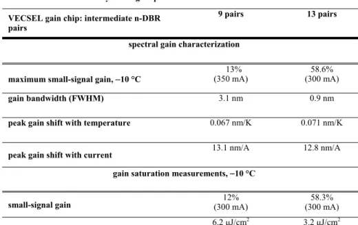
Table 1. Summary of the gain parameters of the two characterized devices VECSEL gain chip: intermediate n-DBR
pairs
9 pairs 13 pairs
spectral gain characterization
maximum small-signal gain, −10 °C
13%
(350 mA) (300 mA) 58.6%
gain bandwidth (FWHM) 3.1 nm 0.9 nm
peak gain shift with temperature 0.067 nm/K 0.071 nm/K
peak gain shift with current 13.1 nm/A 12.8 nm/A
gain saturation measurements, −10 °C
small-signal gain (300 mA) 12% (300 mA) 58.3%
saturation fluence 6.2 μJ/cm
2 3.2 μJ/cm2
With a low-saturation fluence QW-SESAM we passively modelocked the less resonant EP-VECSEL, and generated 9.5-ps pulses with an average output power of 7.6 mW at a repetition rate of 1.4 GHz, which represents the shortest pulse duration from an EP-VECSEL to date.
Even shorter pulse durations and higher output powers should be possible by further optimizing the device performance, especially with regards to (cw) single-mode output power, gain bandwidth and GDD. A low number of n-DBR pairs yields a high gain bandwidth and moderate GDD values, which both favor shorter pulses. On the other hand, the low field enhancement results in less gain. Consequently, the losses of the devices need to be reduced together with the number of n-DBR pairs. One possibility is the reduction of the CSL-thickness to lower the optical loss. Optimizing the SESAM for the resonant EP-VECSEL gain structures will additionally improve the modelocking performance of the devices. A resonant design reduces the saturation fluence of the SESAM. A higher single-mode power enables a stronger saturation of the SESAM and thus a more efficient operation of the laser.
Acknowledgments
The research leading to these results has been partially funded by the European Community’s Seventh Framework Programme (FAST-DOT) under Grant No. 224338, and by the Swiss Confederation Program Nano-Tera.ch, which was scientifically evaluated by the SNSF.