ALA ASIC: A Standard Cell Library for
Asynchronous Logic Automata
MASSAWETsl TEby
AUG 2 4 2010
Forrest Oliver Reece Green
LIBRARIES
Submitted to the Department of Electrical Engineering and Computer
Science
in partial fulfillment of the requirements for the degree of
Master of Engineering in Electrical Engineering and Computer Science
at the
ARCHIVEs
MASSACHUSETTS INSTITUTE OF TECHNOLOGY
June 2010
@
Massachusetts Institute of Technology 2010. All rights reserved.
Author ... .
Departient of Electrical Engineering and Computer Science
March 31, 2010
Certified by.../. . .. t ....
Neil Gershenfeld
Professor of Media Arts and Sciences
Thesis Supervisor
Accepted by
,...Dr. Christopher J. Terman
Chairman, Department Committee on Graduate Theses
ALA ASIC: A Standard Cell Library for Asynchronous Logic
Automata
by
Forrest Oliver Reece Green
Submitted to the Department of Electrical Engineering and Computer Science on March 31, 2010, in partial fulfillment of the
requirements for the degree of
Master of Engineering in Electrical Engineering and Computer Science
Abstract
This thesis demonstrates a hardware library with related tools and designs for Asyn-chronous Logic Automata (ALA) gates in a generic 90nm process development kit that allows a direct one-to-one mapping from software to hardware. Included are basic design tools to enable writing ALA software, the necessary hardware designs for implementation, and simulation techniques for quickly verifying correctness and performance. This thesis also documents many of the hazards and opportunities for improving them including helpful variations to the ALA model, design tool needs, better simulation models, and hardware improvements.
To embody software you could compile a hardware description language to an FPGA or synthesize it all the way to transistors. Alternatively, you could use your favorite high level language and run it on a standard processor. However, the widening gap between traditional models of computation and the reality of the underlying hardware has led to massive costs for design and fabrication as well as numerous issues for scalability and portability. Unlike any of these other approaches, ALA aligns computational and physical descriptions making it possible to use a direct one-to-one mapping to convert an ALA program to a circuit or other physical artifact that executes that program. No unpredictable fitters or compilers are needed and no extra expertise is needed for specific technologies. Similar to Mead-Conway design rules ALA designs trade flexibility for portability and ease of design. Unlike Mead-Conway design rules, ALA designs do not require any further verification-the design rule primitives are logical operations suitable for use in analysis at the algorithmic level. ALA separates many of the scaling issues that plague integrated circuit design
by cleanly separating algorithm design from hardware engineering-improving design
verification, tape-out costs (by reusing masks), yield, portability, and the ability to break designs across multiple chips. ALA designs are not limited to integrated circuits and could just as easily be implemented in microfluidics, magnetic logic, or a lattice of molecular logic gates. Although each of these technologies would require implementing a basic set of gates and tiling rules, hardware (or equivalently software) can be developed using the same deterministic noiseless digital abstraction using the
same design in many different technologies. Thesis Supervisor: Neil Gershenfeld
Acknowledgments
This work was supported by the MIT Center for Bits and Atoms and the U.S. Army Research Office under grant number W911NF-09-1-0542.
I would like to express my appreciation for the support of MIT's Center for Bits
and Atoms and its sponsors and the administrative and academic staff at MIT that have made it possible to be here.
I thank Neil Gershenfeld, my thesis advisor, for his vision and advice. In directing the Center for Bits and Atoms, he has created a challenging and rewarding environ-ment which has nurtured the ideas in this thesis and many others. His guidance has been invaluable in bringing this work to fruition.
I thank Ara Knaian for taking me on as a UROP and introducing me to the Center
for Bits and Atoms which ultimately enabled me to become a part of this amazing team.
I thank the other members of the RALA team including Jonathan Bachrach,
Kail-iang Chen, David Dalrymple, Erik Demaine, Scott Greenwald, Bernhard Haeupler, Ara Knaian, and, Peter Schmidt-Nielsen as well as the members of the larger PHM group for their collaboration, contributions and camaraderie. Without your conver-sations, assistance, and late night food orders I doubt I would have made it through this process.
I thank my friends here at MIT and back in Texas for making sure that my research wasn't the only interesting part of my life.
I thank the many professors and TAs here at MIT that have equipped me with
many of the skills and experiences that have been crucial to my academic career. In particular I would like to thank 6.004, 6.374, 6.375, and 6.376 for key insights into circuit design and computer architectures as well as 6.115, 6.141, MAS.863, and
MASLAB for teaching me how to build stuff.
I would like to thank my parents better than I know how to in words: Thanks
Contents
1 Introduction 13
1.1 Historical Background . . . . 16
1.2 Relationship of ALA to Other Models . . . . 17
1.2.1 RISC Processor Architectures . . . . 17
1.2.2 Asynchronous Logic . . . . 18
1.2.3 Petri N ets . . . . 18
1.2.4 CA Logic . . . . 18
1.2.5 Wavefront and Systolic Arrays . . . . 19
1.2.6 FPGA and Sea of Gates Designs . . . . 19
1.2.7 Dataflow Architectures . . . . 19
2 The ALA Software Model 21 2.1 An ALA Gate Set . . . . 21
2.1.1 BUFFER/INVERTER Gate Behavior . . . . 23
2.1.2 AND/NAND/NOR/OR Gate Behavior . . . . 24
2.1.3 XOR Gate Behavior . . . . 24
2.1.4 CROSSOVER Gate Behavior . . . . 24
2.1.5 COPY Gate Behavior . . . . 24
2.1.6 DELETE Gate Behavior . . . . 25
2.2 Choice of Rules . . . . 25
2.2.1 Ensuring Deterministic Behavior and Allowed Variations . . . 26
2.2.2 ALA Buffer Chain Example . . . . 26 7
3 Example ALA Designs and Tools
3.1 Oscillators and Control Signals ....
3.2 Adder Design ... 3.3 Design Tool . . . . 3.3.1 Hierarchical Designs . . . . 3.3.2 Parametric Designs . . . . 29 . . . . 29 . . . . 31 . . . . 34 . . . . 34 . . . . 35
4 ALA Hardware Design 4.1 Asynchronous Handshaking . . . . 4.1.1 State Storage with C-Elements . . . . 4.1.2 Precharge Full Buffer . . . . 4.2 Gate Layouts . . . . 4.3 Perform ance . . . . 4.4 Design Flow: ALA to Silicon . . . . 4.4.1 Comparison with a traditional design: 3 Bit LFSR 37 . . . . 38 . . . . 38 . . . . 39 . . . . 40 . . . . 41 . . . . 41 . . . . 42 5 ALA Simulation 47 5.1 Discrete Event Model of PCFB . . . . 47
5.2 Simplified Model of PCFB . . . . 48
5.3 TkALA Simulator . . . . 48
6 Alternative Hardware Implementations 51 6.1 Quad-Rail Asynchronous SRAM Half-Buffer . . . . 52
6.2 Using Non-Ratioed Logic for Low Voltage Low Energy Operation . . 53
6.3 Lack of Asynchronous Merge . . . . 55
6.3.1 POLL Gate . . . . 57
6.4 Lack of Wires: Transport Cell . . . . 57
7 Conclusion 59
A Hierarchical Design Example: Scalable Encryption Algorithm Round 61 B Parametric Design Example: Arbitrary Period Oscillator 79
List of Figures
2-1 Ten Implemented ALA Gates and Token Legend . . . . 23
2-2 Initial Condition for Buffer Demo . . . . 28
2-3 Buffer Demo After 1 "Step" . . . . 28
2-4 Buffer Demo After 2 "Steps" . . . . 28
2-5 Buffer Demo After 3 "Steps" . . . . 28
3-1 Bit Loop Emitting (0,1,1,1) Attached to Line of Buffers . . . . 30
3-2 Binary Oscillator Attached to Line of Buffers . . . . 30
3-3 4 State Oscillator and Line of Buffers . . . . 31
3-4 Heat Map of 64 State Oscillator . . . . 31
3-5 42 State Oscillator . . . . 31
3-6 8 Cell Adder . . . . 33
3-7 11 cell adder . . . . 33
3-8 13 Cell Adder . . . . 33
4-1 Basic C-Element built from AND/NOR/SR-Flipflop . . . . 39
4-2 C-Element Oscillator . . . . 39 4-3 PCFB Schematic . . . . 40 4-4 BUF Gate . . . . 44 4-5 CROSS Gate . . . . 44 4-6 NAND Gate . . . . 44 4-7 XOR Gate . . . . 44 4-8 COPY Gate . . . . 44 4-9 DELETE Gate . . . . 44 9
4-10 Main Tile For NAND Cell 4-11 4-12 4-13 4-14 4-15 4-16
Overlay Tile With Wires For North Input Overlay Tile With Wires For West Input 1 Overlay Tile With Wires For East Output Combination of All Tiles . . . . LFSR as ALA . . . . LFSR as Layout . . . .
5-1 Full PCFB State Diagram . . . .
5-2 Simplified PCFB State Diagram . . . .
Quad-Rail Asynchronous SRAM Half-Buffer Voltage Scaling for 4-bit 3-tap FIR Filter . .
Non-Ratiod PCFB Design . . . . Heat Map of a Simple Multiplier . . . .
and Connections
A-1 Scalable Encryption Algorithm Round . . . . .
B-1 42 State Oscillator . . . . . . . . 4 5 . . . . 4 5 . . . . 4 5 . . . . 4 5 . . . . 4 5 . . . . 46 . . . . 46 . . . . 48 . . . . 4 9 6-1 6-2 6-3 6-4
List of Tables
3.1 Relative Adder Performances . . . . 32
4.1 Cell Performance Numbers . . . . 41
4.2 Comparison of ALA Design and Custom Design Before Layout . . . . 43
Chapter 1
Introduction
Many computational tools, with applications ranging from computer graphics to cryp-tography, travel the road from clunky prototype to miniaturized commodity hardware. In this process they can be implemented in an easy to distribute fashion as a program for a desktop computers, altered to run in specialized but easy to acquire customiz-able hardware, such as field programmcustomiz-able gate arrays (FPGAs), and reimplemented and fabricated as application-specific integrated circuits (ASICs). Though the de-velopment and deployment costs increase with specialization of the hardware, the performance benefits can be staggering. Unfortunately efficient implementations for each class of hardware typically require substantial redesign to cater to the quirks of the technology. Asynchronous Logic Automata (ALA) is a new model of computa-tion that attempts to approximate the physical constraints common to all possible hardware into single easy to manipulate abstraction. The basic idea (detailed in chapter 2) is to allow the designer to place a network of simple processing elements in a physical space and connect them together. Forcing the designer to maintain physically realistic spatial relationships ensures that it will be possible to generate a hardware implementation regardless of the underlying technology-working with everything from reconfigurable hardware, to custom integrated circuits.
Even if hardware expertise is available, portability can still be an issue. In the-ory, a design done for one integrated circuit (IC) process using Mead-Conway design rules, can still be used after feature scaling and other improvements. In practice,
changes in gate carrier mobility, interconnect resistance, relative capacitances, etc. can easily upset the delicate balances in a complex IC design. Simply scaling designs will not take full advantage of things like more metal layers and variable threshold transistors or handle the issues that arise in deep sub-micron technologies. This thesis demonstrates a standard cell library implemented in a generic 90nm process development kit of ALA cells, a design abstraction that allows a direct one-to-one mapping from software to hardware that is portable to different processes scales as well as radically different hardware such as microfluidics, magnetic logic, or even technologies not yet predicted. This mapping from software to hardware partitions algorithmic design issues from technology specific engineering details so that the de-sign of application-specific integrated circuits (ASICs) can be done portably without regard to the underling process technology. Although there are an assortment of pos-sible high level tools and languages to improve performance and ensure correctness of the algorithms, hardware synthesis of ALA designs is simply an assignment of tiles to locations and requires no compilers, fitters, or post-design verification.
ALA is based on the assumption that storing information requires a minimum
energy per bit and that the universe allows only a finite energy density (and thus in-formation density) and only local interactions. It excludes the potential for quantum-coherent computations as such mechanisms are currently impractical and poorly un-derstood. It also assumes that computation and communication consume power. While charge conserving techniques based on reversible computing have been used to reduce power consumption (for example [18,22]) they are not considered in the ALA model. When creating fully reversible programs with predicted or current technology (gigahertz frequency CMOS for example) it is unclear that it is possible to achieve
high enough
Q
factors that resetting a computation by reversing it would be moreefficient than simply dissipating a cycle's worth of power. It may be possible to use charge conserving techniques to improve power consumption in the cells (a topic of current research), but this would be a hardware optimization rather than a change to the programming model. Finally, it assumes that it is possible to use external entropy sources or pseudo random number generators if probabilistic behavior is needed.
The ALA model has been engineered rather than derived. Although finite infor-mation density and local interactions are fundamental properties of physics (perhaps excluding certain quantum phenomena), ALA is far from the only possible model that respects those. It would be possible to add or remove some cell types or make individ-ual cells more complex or simpler while still respecting the fundamental design goals of ALA, however through trial and error we have found what we believe is a good balance between simplicity of the cells (to allow portability to other technologies), ease of design (by providing logical operations as the primitives), and fidelity to the underlying fabrication capabilities (to improve efficiency). Many of the similarities between ALA and other models of computation come from using the same approach for a given trade off. Although the choice of rules is not absolute, there are important properties that must be maintained to ensure correct operation and to respect the physics.
When we use a specific technology to design a computer we limit our choice of building blocks in exchange for simpler abstractions and easier fabrication. You can build a computer out of transistors in silicon, microfluidic channels [15] in glass, or tinker toys and strings [9]. For each technology, a reasonable approach is to start with a library of basic components (transistors and wires, different shapes of channels, or memory spindles and output ducks) and use those to build up desired functions. However, by the time we write algorithms for these computers, we are many layers of abstraction from the underlying physics. While these abstractions are necessary to mantain the sanity of the programmers, they can make it difficult to write effi-cient programs. For the von Neumann programming model, hardware designers have worked hard to preserve the fiction of fast sequential operation with constant time access to all memory, but for a modern desktop this is far from true. Caching, branch prediction, parallel dispatch, speculative execution, register renaming, pipeline stages, and the myriad of other techniques in the processor architect's tool bag make it nearly impossible to predict when, in a given program, it will proceed immediately to the next instruction or spend tens of millions of cycles swapping in a new page of memory from disk. ALA attempts to resolve this issue by exposing the same building blocks
to the programmers that are available to the hardware designers. While there are necessarily approximations to ensure usability, care has been taken to ensure that these approximations don't limit the programmers ability to predict the final per-formance of their algorithm. Many of the same techniques that we see in processor architectures would likely be components in higher level ALA descriptions.
Presented in this thesis are a set of designs and tools for creating ASICs from
ALA designs including:
1. Several simple ALA modules as well as a minimal programming library for
expressing hierarchical ALA designs
2. Circuit designs for a library of ALA cells that can be tiled to generate an ASIC layout
3. A graphical simulator for ALA that does performance modeling orders of
mag-nitude faster than general techniques
4. Suggestions for several alternative designs and possible improvements
1.1
Historical Background
The foundations of most modern computer architectures can be traced back to work started by John von Neumann in the 1940s [20] and to this day the majority of com-puters use the same basic principle of a single active processing element connected to a large bank of passive memory. His later work on Cellular Automata (CA) was in-spired by his interest in self reproducing machines, but in the process he demonstrated the possibility of computation in CAs. Later work by Roger Banks [2], published in
1971, demonstrated universal computation with simpler symmetric rules. Of the
many other CAs that have been shown to be universal, one of my personal favorites is John Conway's Game of Life [10], which was a major inspiration for my initial interest in computer science. While CAs were not attractive for early computers, the development and scaling of integrated circuits changed many of the engineering
constraints. Instead of expensive, power-hungry vacuum tubes connected by fast, cheap and nearly arbitrary wiring, designs were using cheap and power-efficient tran-sistors with increasingly difficult routing and wire delay issues. Unfortunately, the von Neumann processor architecture, which is dominant even today, assumes that in-terconnect is free and has no way of expressing spatial constraints. The need for new
computing abstractions was recognized early in the 1980s
[8]
and inspired dataflowmachines, the CAM-8, and the Connection Machine among others. In many cases,
their lack of success arguably stemmed from non-technical issues [17]. The same
scaling trends that began to make these alternate architectures favorable have con-tinued to progress. Even mainstream hardware has had a distinct trend towards more parallel computing, but progress has been slow on better parallel programming ab-stractions and nearly nonexistent on spatial computing models. At today's gigahertz clock speeds, speed of light limits can be significant even over centimeter distances. The continued scaling of process technologies and clock speeds will make spatial con-straints significant well below the level of a chip. There are predictions [1] that in deep submicron designs less than 1% of a chips area will be reachable in a single cycle. These trends have lead to my research group's interest in physically based models of computation. Notable prior work in which ALA was developed includes [3,6,7,11].
1.2
Relationship of ALA to Other Models
ALA has many similarities with other models of computation. This is partly from
convergent engineering under similar constraints and partly from using good ideas where they are compatible. In this section we discuss similarities and differences with selected models. More details on many of these relationships and others can be found in [7]
1.2.1
RISC Processor Architectures
ALA can be considered as an extrapolation of the current trend for multi-core RISC
program. Unlike a single processor, which becomes progressively more difficult to scale up in speed, ALA performance scales by spreading computation over more cells.
ALA designs work at a fine enough granularity that many of the tricks that could
be used to speed up a traditional processor, like pipelining or speculative execution, can be implemented above the ALA abstraction. This makes it possible to integrate these techniques where they will help without being forced to pay their overhead in all cases.
1.2.2
Asynchronous Logic
Asynchronous logic is not a new concept, but making use of it often involves specific expertise and significant caution to ensure correct operation. The careful choice of
ALA gates and design rules encapsulates all of the non-deterministic behavior to
ensure that designers do not need to worry about rare edge cases but can still have most of the benefits to power from only consuming dynamic power where useful computation is taking place and robustness to power supply or process variations.
1.2.3
Petri Nets
Although similar to Petri nets, in that cell updates are activated by the presence of tokens on their inputs and are allowed to happen in any order, the cell update rules have been carefully restricted to enforce deterministic results regardless of the firing order. It is worth noting that there are some situations where this is not beneficial, but a possible fix for this is described in section 6.3.
1.2.4
CA Logic
Arbitrary computation has been demonstrated in many different cellular automatons (notably [2], [19], [5]); however these typically take dozens to hundreds of cells running for many generations to perform even a single logical operation or only work for very specific kinds of computation (i.e. [14]). In ALA the primitive rules are chosen to try and minimize the cost of implementing practical systems by allowing a single
cell in one step to perform a logical operation. This is a significant benefit both for simplicity of creating designs from the ALA gates as well as flexibility in implementing the underlying hardware. Finally, the global clock needed in synchronous CAs isn't physically realistic and is avoided by using ALA without the complications that arise in other asynchronous CAs such as [13].
1.2.5
Wavefront and Systolic Arrays
ALA also has a strong resemblance to wavefront and systolic array processors, but
there are no restrictions on how information flows through the system allowing arbi-trary classes of computation with irregular data dependencies.
1.2.6
FPGA and Sea of Gates Designs
ALA design bears a strong resemblance to digital circuit design and in particular to sea
of gate design styles. Similarly, the reconfigurable version of ALA (RALA) resembles FPGAs. However, ALA designs have a direct one-to-one mapping to the hardware that does not depend on fitters and their synthesis capabilities. Even for experienced users it can be difficult to account for the impact of fitter behavior on a design. Unlike in an FPGA, where the capabilities are often chosen based on what is efficient to implement in a specific technology, the rules for ALA are chosen to ensure that they can be implemented in many different technologies. This makes ALA designs substantially more likely to be portable. Section 4.4.1 compares a very simple design done in ALA and with standard synchronous gates. Although the custom design has better performance, after accounting for improvements from chapter 6's designs and clock generation and distribution costs, the ALA design would likely be competitive with traditional FPGA and sea of gate implementations.
1.2.7
Dataflow Architectures
ALA gates are dataflow architectures in that computation is triggered by the flow of
architec-tures are solved by limiting cells to local interconnect and allowing the designer to choose how to handle that constraint.
Chapter 2
The ALA Software Model
ALA is a programming model based on cellular automata, which consists of a regular
grid of cells. Each cell has a permanent configuration or 'gate' that controls how it will pass and accept chunks of information or 'tokens' from adjacent neighbors. Different gates can pass tokens unchanged, fanout tokens, compute logic functions, or create and destroy tokens. Gates are analogous to the primitive instructions on a processor. Unlike a petri net, tokens contain a small amount of internal information on which the logic functions are computed or behaviors are controlled. Gates do not operate in lock step and can operate at different speeds, however their update rules wait until enough tokens have arrived to produce a deterministic result.
This chapter focuses on a specific ALA programming model describing the partic-ular gates that were developed and how they work. This chapter also discusses some of the motivations for choosing this specific set of gates.
2.1
An ALA Gate Set
The gates used here are very similar to those used in [3,6,11,12] but have been revised slightly to make the hardware simpler and take advantage of things that were easy to implement in CMOS. The variations used here likely bring the rules closer to a lowest common denominator for many representative technologies. Slightly different optimizations may be possible in other technologies (microfluidics, magnetic logic,
etc.) however it is difficult to predict exactly how they would differ before doing those designs. Comparing possible optimizations across a broad spectrum of technologies remains a topic for future work.
These ALA designs use a rectangular 2D grid of cells that can be set as one of ten different gates with outputs going to adjacent neighbors (not including diagonals). Unlike the reconfigurable variant described in [11], the cell configuration is hardwired and cannot be changed short of making a new chip. Cells communicate by passing boolean tokens to each other that can be either true (T) or false (F). The output of a cell doesn't need to have a token at all times and can be empty (X). Inputs and outputs to an ALA program are done by special cells that exchange tokens with the outside world. One could imagine having pixels in a display or some kind of sensor at regular intervals throughout the ALA grid or a network connection attached at a specific point. Figure 2.1 shows the symbols for tokens and the set of gates we implemented. The basic operation of all of the cells is relatively uniform throughout. Each cell waits until all of the needed input tokens have arrived from neighbors, consumes them, and emits new output tokens. In the CMOS implementation, inputs are consumed by signaling over an acknowledge wire connected to the cell that emitted that token which then clears its output. For a microfluidic implementation, input tokens might literally be physically consumed. The implementation used here differs from those described in [6,11,12] in that cells may produce outputs before all the inputs arrive if it is possible to deduce what the output token will necessarily be. For example if one of the inputs to an AND gate is an F (false) token, then the cell may produce an output of F before the other input arrives. This is called short circuiting. This is more powerful than previous versions of ALA because any design that would have worked with older versions will still produce the same outputs but not necessarily as quickly. This can allow some designs to function which would have stalled indefinitely without short circuiting. This is unlikely to be a problem unless the design was connected to an external peripheral which was time sensitive. Arguably, this is a generalization where cells are allowed to take on faith that the other input would eventually arrive. This idea can be further extended by allowing acknowledge signals to propagate up
Logic Function
Token
Tokens &
Manipulation Directions
BUFQ
AND
E
CROSS
0/F
INV>
NAND
D
COPY
41
/T
OR
F
DELETE
empty
XOR)D
NOR
1DW
E
_S
Figure 2-1: Ten Implemented ALA Gates and Token Legend
empty inputs as antibits.
The ten types of gates are divided into 6 sub-types. Because of the dual rail encoding of tokens in the CMOS implementation, inverting a token can be done by swapping how the inputs are connected. By inverting inputs or outputs, the buffer and inverter have equivalent implementations. Likewise, AND/NAND/OR/NOR are equivalent by DeMorgan's law. Except for the CROSSOVER, all gates have symmet-ric outputs that can be fanned out to up to two different neighbors.
2.1.1
BUFFER/INVERTER Gate Behavior
The BUFFER/INVERTER gate is a one input gate that waits until the input has a token and the output is empty and then emits it (or its complement) to the output and acknowledges the input. A chain of BUFFER gates connected to each other can hold a series of tokens. A simple way to generate a periodic sequence is to have a loop of BUFFER gates that have been initialized to your desired sequence. As the sequence travels around the loop, a copy can be fanned out. It is important to note that in addition to allowing temporary storage of tokens, the BUFFER/INVERTER gate is necessary because interconnect is only local in ALA, meaning cells can only
communicate if they are adjacent to one another. There is no wire primitive-cells must be connected by a chain of BUFFER gates.
2.1.2
AND/NAND/NOR/OR Gate Behavior
The AND gate is a two input gate that waits until at least one F input or two T inputs have arrived and the output is empty. It then emits a F output if there was an input of F, and a T output if both inputs were T. After the output has been generated and both inputs have arrived, they are acknowledged. NAND, NOR, and OR can be constructed from AND by using DeMorgan's law.
2.1.3
XOR Gate Behavior
The XOR gate is a two input gate that wait waits until both inputs have arrived and emits their exclusive or, i.e. it emits an F if both inputs match and a T if they do not match. Unlike the AND gate, it does not short circuit.
2.1.4
CROSSOVER Gate Behavior
The CROSSOVER gate is essentially two BUFFER gates in the same position. It waits for an input and emits the input in the same direction it was going. So if an input arrives from the east of the CROSSOVER gate, the gate emits it to the west.
2.1.5
COPY Gate Behavior
The COPY gate is a two input gate with asymmetric inputs called control and data. Control selects whether or not to copy the data input. So when a T token arrives at the control input, the token on the data input is copied to the output, but not acknowledged and therefore remains on the data input. If more T tokens arrives on the control, the gate will continue to emit copies of the token waiting on the data input. An F token at the control input causes the data input to be passed on as it would be in a buffer and be acknowledged. If you consider the BUFFER gate to pass
tokens across space, the COPY gate passes them across time. The COPY gate always emits the same number of tokens as it consumes via the control input, but consumes only as many tokens via the data input as it receives F tokens on the data input.
2.1.6
DELETE Gate Behavior
The DELETE gate is the dual of the COPY gate. Like the COPY gate, the two asymmetrical inputs are called control and data. Unlike the COPY gate, control selects whether or not to delete the data input. When a T token arrives at the control input, a token is acknowledged from the data input and no new tokens are emitted. When an F token arrives at the control input, the data is passed on with the same behavior as a COPY gate when it receives an F control token. The DELETE gate always consumes the same number of tokens on the control and data inputs, but emits only as many tokens as it receives F control inputs.
2.2
Choice of Rules
There is a minimum complexity/variety necessary to enable universal behaviors, but this is fairly low. For example, Banks demonstrated universal logic in a 3 state 4 neighbor synchronous CA [2] (which can in turn be implemented by 2 state 4 neighbor CA). However in a system like that, many cells must undergo many steps to compute even a single binary operation. One of the goals for ALA was to ensure that implementations of practical sorts of systems could be done with reasonably small overheads. To allow optimization below the granularity of the cells, we wanted cells that were as complex as would be useful. On the other hand, very complicated cells would be difficult to analyze and implement in other technologies and might have capabilities that would be wasted. The eventual choice was to use two input boolean operations as the core granularity.
Although in general, NAND is sufficient to construct universal Boolean logic func-tions, within ALA we also need explicit support for wiring and crossovers. To fully take advantage of the asynchronous nature of the circuits, we need to be able to pass
information between domains that are operating at different rates. The COPY and
DELETE gates provide this functionality and the CROSSOVER gate ensures that
we can route signals in different domains across each other without worry about their relative rates as would be necessary using XORs. Thus the true minimum set of gates would contain NAND, CROSSOVER (which could be used as a buffer), COPY, and
DELETE. However, for ease of design we choose to include the other logic functions
as well. Since the hardware uses a dual rail encoding for the logic in which inver-sion can be done by swapping where inputs or outputs are connected, AND, NAND, OR, and NOR all use the same circuit. It would have been possible to include a much larger set of gates, but finite design effort and a desire for compatibility with future reconfigurable designs motivated us to keep the number of gates close to the minimum.
At least in CMOS, it is likely that actual wires could be used to connect over dozens or possibly hundreds of cells without significant degradation of performance. This would reduce power consumption substantially.
2.2.1
Ensuring Deterministic Behavior and Allowed
Varia-tions
The choice of gates for ALA can not include anything that can be affected by when tokens arrive. This is to avoid introducing technology dependent design constraint based on how fast each gate processes inputs. The current design ensures this by using what is close to a single-assignment single-reader model one might see used for parallel programming. New values can be written, but only after the old one has been garbage collected by acknowledge signals.
2.2.2
ALA Buffer Chain Example
This section will provide an example of the basic operation of an ALA design. Here is a diagram of four ALA cells (labeled A,B, C, and D). The arrows between cells represent state storage elements for tokens. Red arrows indicate where a True token is
stored, blue arrows indicate where a False token is stored, and gray arrows indicated that no token is stored at that location. The three cells labeled A, B, and C are buffer cells that wait until their input has a token and their output is empty. The fourth cell, labeled D, is an AND cell that atomically consumes a pair of input tokens and produces a single output token that is a logical AND of the two consumed tokens.
Figure 2.2.2 shows the initial state of the cells. Figure B shows the same cells again a short time later. We see that the True token waiting at the input of cell B has been propagated to cell C.
After another small amount of time, figure 2-3 shows both cells A and C have fired propagating their tokens onwards. Note that because the cells are operating asynchronously there is no defined order for these events. (In the hardware described later in this document the token would probably propagate all the way to cell D by the time the acknowledge logic cleared the token from the input.) However, regardless of the order of these updates, the next token to arrive at cell D will be a True token. Eventually the two tokens will end in the configuration shown in figure 2-4. The True token waiting at the input to cell D will not propagate through the AND cell labeled D because it must wait until both inputs are present. Similarly, cell C cannot propagate the False token from its input because it is blocked by the token waiting in front of cell D.
4*
0
Figure 2-2: Initial Condition for Buffer Demo
0
0 4D
Figure 2-3: Buffer Demo After 1 "Step"
0
4*
0
D
Figure 2-4: Buffer Demo After 2 "Steps"
0
0
Figure 2-5: Buffer Demo After 3 "Steps"
0
1*
4*
0
4*
0
4*
4*
0
4*
lw O .. - - .. ... .... ... .... ...lq&
Chapter 3
Example ALA Designs and Tools
This chapter presents a few simple examples of ALA designs and tools. The devel-opment of better design tools and more efficient designs are active areas of research and have progressed beyond what is described in this chapter, however these designs offer a good introduction to how gates can be combined and used and some minimal requirements for design tools.
3.1
Oscillators and Control Signals
Transporting data and performing computations have roughly equivalent costs in the
ALA universe so for many applications it is useful to work with serial streams of data.
This creates a trade off between throughput of blocks and their area and complexity. While doing serial processing, it is often necessary to have a periodic control signal (for example to mask out carry bits in a stream of fixed width additions so that the overflow doesn't end up in subsequent calculations). A simple solution for this is to create a loop of BUFFER gates initialized to the desired sequence.
This structure can be initialized to hold an arbitrary pattern which will be emitted at the output and loop back around so that it is repeated. However, many situations do not call for an arbitrary sequence but instead need a single False token in the loop or similar. For these situations, filling the entire bit loop with the pattern costs n2
o+o+0+0
+
t
+++0+ot0to0o0+t+ot+oto0
Figure 3-1: Bit Loop Emitting (0,1,1,1) Attached to Line of Buffers
>0
Figure 3-2: Binary Oscillator Attached to Line of Buffers
around the entire ring every cycle) and linear space. However, we can generate a signal with an arbitrary period with a constant power cost per bit and logarithmic space cost by building a hierarchical oscillator. We start with a simple 2 state oscillator as shown in figure 3.1. A short set of buffer cells has been attached to the output to illustrate the generated output.
Now there are two units that we will add to this. The first is a bit doubler that emits two copies of each input it receives. The two cells on top form another oscillator that produces a stream of alternating True/False tokens. These feed into the control of the copy at the bottom which will duplicate the data input on the True tokens and pass it through on the False input which has a net result of creating two copies of each input token. One of these with a binary oscillator connected to the input will produce two True tokens followed by two False token, as show in figure 3.1, for a period of 4 tokens.
By chaining together these bit doublers we can generate any period that is a power
of two. Because each doubler only fires half as often as the one before it, the total power is a geometric sequence summing to a constant. Figure 3.1 shows a heat map of an oscillator indicating the relative amounts of power consumed in each cell (red is most, blue is least).
While power of two length sequences are sufficient for many situations, we may
>0
>
O
04C+040+00+0+040+040+#0
Figure 3-3: 4 State Oscillator and Line of Buffers
Figure 3-4: Heat Map of 64 State Oscillator
also want to be able to generate sequences with arbitrary periods. A circuit that copies the next bit after a False-True sequence will effectively add one to the pe-riod. Combining this with the doubler makes it possible to generate sequences of arbitrary periods. Appendix B shows a parametric design that generates oscillators with arbitrary periods.
3.2
Adder Design
An important aspect of the ALA architecture is that it allows trade-offs between energy, throughput, and area even for fairly basic primitives. The following are
> 0 D+> 0 0 D+> 0
0+e+e+Oog+re+ +3+o+-54+2+St+atOc+l+l
Figure 3-5: 42 State Oscillator
... . ... ... ..-- -- -- - ... ...
Cells used Throughput (Steps) Throughput Energy/Bit (pJ)
8 1/2 773 MHz 1.51 11 2/3 781 MHz 2.68
13 1 1.24 GHz 3.00
Table 3.1: Relative Adder Performances
three different adder designs which range from smallest size and energy per token through two larger and higher power designs with better throughput. The smallest design, shown in figure 3.2 was created by hard-earned insight about how to order the intermediate steps of the computation to preserve intermediate information, as well as lots of trial and error focused only on size. It has the lowest throughput. The intermediate design in figure 3-6 lays out the expected operations along a diagonal to try and ensure uniform buffering depth. The largest and fastest design from [12] shown in figure 3-7 used graph analysis techniques to add the exact buffering needed to compensate for the feedback of the carry bit and achieve perfectly equal buffering with maximum performance.
The following chart shows their relative performance in Specter simulations. Here step throughput refers to the steady state ratio of output tokens to updates if all cells are updated simultaneously in a synchronous fashion as discussed in [12]. A graphical representation of the step throughput can be seen in the spacing of tokens on the output buffers in figures 3.2, 3-6 and 3-7, where the maximum throughput would be 1 token every other cell.
The difference between the step throughput and the predicted throughput from circuit simulations likely stems from optimizations in the circuit design that allow to-kens to propagate through ready cells faster than the full handshake time. By optimiz-ing our design to allow this, we reduced the cost of bufferoptimiz-ing mismatch and decreased latency substantially. However in comparison to each other, the increased area and power usage still provide a significant speed improvement. Although counterexamples could likely be constructed, this indicates that even very simple performance metrics could be useful to compare designs across technologies.
0+0+o+c+DD+D
0+0+0++4+40+0+0+0+0+0440+04
Figure 3-6: 8 Cell Adder
0
0
0 040
474+47
0+4
D4D
o
+o+o0o~o+oo+o4o040+
Figure 3-7: 11 cell adder
0
0
0
0+0
0+47
0o+om*mO*O+0+0*oEO+0o
Figure 3-8: 13 Cell Adder
-3.3
Design Tool
While pencil and paper or your favorite vector graphics program are reasonably useful for prototyping designs, a more structured approach is necessary to get designs into a format suitable for simulation or automatic processing. Many designs can also be expressed with repeating structures or can be parametrized in terms of things like word length or important constants. While more specific tools are being developed, the designs in this document were generated by Python code that makes calls to the simulator to define the initial cell positions. The choice of language was nearly arbitrary, but the use of a programming language allows substantial flexibility for ways to describe hierarchical and parametric designs. Although working in this fashion requires substantial visualization skills (and often a good bit of debugging), it makes it very easy to add new design capabilities simply by writing more Python modules. For example, I implemented a simple search that builds a chain of buffers along the shortest unoccupied path between two cells. In their current state using these tools is analogous to using an assembler. It is possible to specify a design if you know exactly what you want, but there are no safety nets. One could easily imagine adding a simple type system to help ensure that modules were being connected correctly or automatically doing buffering checks that identify sections where mismatched data path lengths could harm performance to try and come closer to a high level language. Tackling this issue fully would be a substantial research project on its own. The tools used here are more analogous to an assembler than a high level compiler, but they still allow moderately complex designs with the ALA gate set.
3.3.1
Hierarchical Designs
One very important feature of high level languages is the ability to abstract away complex functions and later refer to them as primitive operations. One of the first extensions I did was to create a part class that allows cells or other parts to be added using a local coordinate system. A part could than be instantiated at any position, rotation, or reflection. This serves the same role as function calls in a high level
language by encapsulating complex behavior in a way that is easy to reference multiple times. It also turned out to improve readability of the generated designs substantially. Simply coloring the backgrounds for different parts made it much easier to see how the modules were connected to each other. Interestingly enough, part shapes tend to be sufficiently distinct that it was possible to recognize them without any additional markings. Admittedly, knowing what the parts do requires either careful examination or prior knowledge.
3.3.2
Parametric Designs
A feature that will be useful to preserve in future design tools is the ability to do
parametric designs. The spatial structure of ALA naturally lends itself to graphical design tools, but there is a class of designs that are not readily possible with a direct graphical description. The appendix shows an example of this in a parametric design that creates oscillators with arbitrary periods. The simple addition of repeating tiles covers a broad class of designs, although there are examples where more complex behaviors can be critical. The oscillator is a simple example, but more complex ones could include the Fast Fourier Transform and many examples from cryptography. The ability to optimize away unneeded data paths can represent substantial savings as each "function call" requires space to be allocated for the module that computes that function. On the other hand, design with graphical primitives has the advantage of being much more intuitive. The balance between graphical intuition and descriptive flexibility remains an interesting question for future research.
Chapter 4
ALA Hardware Design
The asynchronous aspect of ALA could be implemented in traditionally clocked logic with token state simply remaining unchanged when cells are not ready to update. Unfortunately this consumes dynamic power even when cells are idle and requires a globally distributed clock. In addition, having cells operate in lock step greatly in-creases the sensitivity of performance to careful design, as shown with the adders. A clocked design would likely be worth exploring to see to what extent the simpler logic enables faster operation or lower dynamic power. The current designs uses a Quasi Delay Insensitive (QDI) style. In many ways QDI is the "purest" kind of computa-tionally universal asynchronous logic in that it makes the fewest assumptions about the underlying technology. While this made design easier and increases portability and reliability, subsequent experiments predict that using a Self-Timed logic style could result in substantial area savings and an additional 30% improvement in power and throughput [3]. Other designs in progress, include one with carefully selected representations for the internal signals to reduce power and area that avoids ratioed logic to allow lower operating voltages for improved efficiency at lower speeds, as well as a design based on SRAM cells that could substantially reduce transistor count. At this time, these designs are incomplete and remain as subjects for future work.
4.1
Asynchronous Handshaking
Synchronous circuits are carefully designed to ensure that all signals will be ready before the next clock edge. In asynchronous circuits, a local ready signal is computed that replaces the clock. This can be done with a carefully engineered delay element or a data representation, like the one used here, where intermediate and final values can be recognized. In our design we used a dual rail data encoding where two wires, one for 0/F and one for 1/T, represented the state of each token. When both of these lines were low the port is said to be empty or X. If the T or F line was high that was the state of the port. Both lines high was an invalid state. We used a four phase handshake where a third acknowledge line would go high to signal ready for a new token and go low to indicate after the new token had been latched.
4.1.1
State Storage with C-Elements
Each ALA cell needs to hold a small amount of state which would normally be held
by a register or latch in regular sequential logic. However, in asynchronous logic there
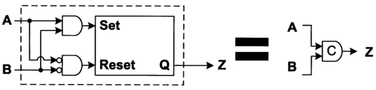
is no global clock to coordinate operation among registers as normal. To compensate for this a common component in asynchronous logic is a C-Element. Instead of using a single input to trigger when data begins being passed to the output it waits for a combination of inputs to be set or cleared and then transitions or otherwise holds the current state. Careful design of the logic ensures that the computation remains within the stable inputs until it is complete, which then triggers the output to change and cascades into the next phase of the computation. There are numerous ways to implement C-Element (for some examples see [16]). Here is an inefficient but easy to understand C-Element constructed from an AND gate, NOR gate (AND with inverted inputs), and a Set Reset Flipflop. When both inputs or set or cleared the output will likewise be set or cleared.
The C-Element is a powerful component for the design of asynchronous circuits. For example, the following circuit is an asynchronous 4 state oscillator. It is left as an exercise for the reader to understand the exact operation. It is very similar to the
- -I~ F
I - - - - - - - I
A
C
z
B
Figure 4-1: Basic C-Element built from AND/NOR/SR-Flipflop
handshake mechanism in a precharge full buffer described in the next section if you want a hint.
Figure 4-2: C-Element Oscillator
4.1.2
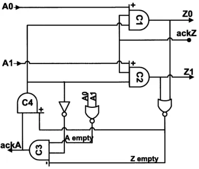
Precharge Full Buffer
The core of each cell centers around a precharge full buffer similar to [21]. This circuit implements a 4 phase handshake. In the idle state C1 and C2 are reset and C3 and C4 are set. In this situation ackA (C3) will be high to signal that the buffer is waiting for a new input. The handshake works as follows:
1. New input arrives at either AO or Al triggering C1/2 to emit a new Z value if
ackZ is high
2. The new Z value causes ackA to go low by way of Zempty resetting C4 in the process
3. Low ackA from this buffer causes the preceding buffer to clear this buffers input Z
4. Aempty going high sets ackA (signaling ready for new token) and returns the cell to idle
Figure 4-3: PCFB Schematic
The full state diagram for the PCFB is shown in figure 5.1. For more details of operation, information on incorporating logic, and the modifications to implement COPY and DELETE cells see [4].
4.2
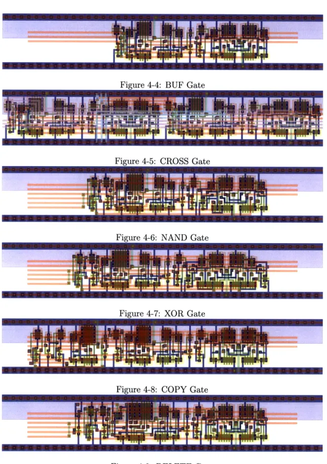
Gate Layouts
Figures 4.2 to 4-8 show the full layouts for the 6 gates classes. The BUF Gate can be converted to a INV gate by swapping the T/F token wires of either the input or the output. Similarly the NAND gate can be converted to AND, OR, or NOR. Fanout requires the addition of a C-Element which is not shown.
4.3
Performance
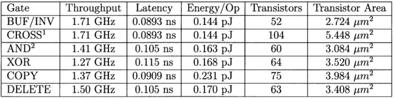
After finishing the layouts we used the Spectre simulation tool to estimate their performance. Table 4.3 shows our results. Throughput is the maximum rate at which a gate can process available tokens. Latency is the time between when the inputs arrive and when the output is emitted. Because outputs can be emitted immediately before the full handshake is complete, tokens can propagate through empty cells much faster than the cycle time that limits throughput. This significantly decreases the performance impact of buffering mismatches. Energy/Op is the amount of energy consumed when a cell fires. Transistors measures the total number of transistors needed for each kind of cell. Transistor Area is the total area of the transistor gates (the control terminal of the MOSFET, not the entire cell). Cells are placed on a lattice that is 28.2 pm by 4.295 pm to accommodate the largest cell (the crossover)
and thus occupy 122 pm2 each.
Adding fannout to a gate is done with a single C-element and increases the
Ener-gy/Op by about 0.039 pJ and decreases the Throughput by 10 to 15%.
Gate Throughput Latency Energy/Op Transistors Transistor Area
BUF/INV 1.71 GHz 0.0893 ns 0.144 pJ 52 2.724 pm2 CROSS1 1.71 GHz 0.0893 ns 0.144 pJ 104 5.448 pum 2 AND2 1.41 GHz 0.105 ns 0.163 pJ 60 3.084 pm2 XOR 1.27 GHz 0.115 ns 0.168 pJ 64 3.520 pum2 COPY 1.37 GHz 0.0909 ns 0.231 pJ 75 3.984 pm2 DELETE 1.50 GHz 0.105 ns 0.170 pJ 63 3.408 pum 2
Table 4.1: Cell Performance Numbers
4.4
Design Flow: ALA to Silicon
We have developed a library of ALA cells in a generic 90nm process that can be arbitrarily tiled. The first layer of tiles are function tiles that select an operation (i.e.
'Energy/Op for the CROSS cell is for 1 token in either direction.
2
AND, NAND, NOR, and OR as well as BUF and INV have equivalent hardware; logical inversion
NAND, COPY, CROSS) as well as choosing between one or two outputs. Directly
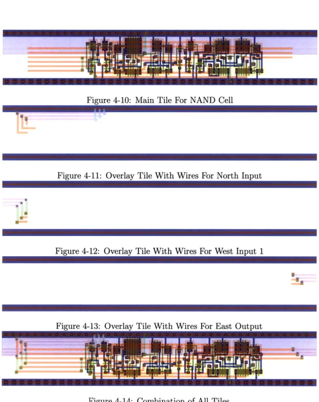
on top of this are tiles that connect inputs and outputs with their counterparts in adjacent tiles. Figure 4.4 shows the tiles needed to create a NAND cell with inputs from the east and north. While standardizing the locations of the input and output ports and adding a separate layer of wiring was largely motivated by wanting to avoid doing new layouts for every combination of inputs, it illustrates the ease with which ALA could be used in a sea of gates style fabrication process. All ten of the implemented function tiles could be encapsulated with just 4 tiles and a wiring layer that can rearrange inputs. AND, NAND, OR, and NOR are equivalent and would work as a buffer/inverter if the inputs were connected in the same direction, XOR has different logic and could serve as the second buffer in a crossover by connecting one of the 0 wires in the input to the ack pin. COPY, and DELETE would be the remaining two tiles. With fairly minor optimizations it would likely be possible to get this area overhead within a factor of two of the current tiles sizes. Using these superfunction tiles, it would be possible to fabricate custom ALA ASICS with only one or two custom masks which would drastically reduce cost (in both money and time) of fabrication.
Currently, the process of selecting and placing tiles is manual, but because of the direct one to one mapping to the hardware, the only obstacle to automating this process is being able to manipulate the appropriate file formats. As it stands, I was able to design, layout, verify, and simulate a small LFSR in less than two and a half hours. The majority of that time was spent on tracking down a bug where I had used two input tiles that connected to the same side of the function tile and on setting up simulations. Figure 4.4 shows the ALA design for a three bit LFSR and its hardware layout.
4.4.1
Comparison with a traditional design: 3 Bit LFSR
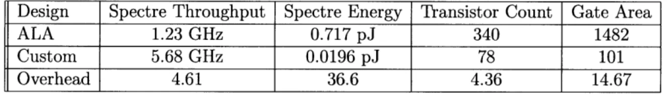
For comparison with existing techniques, I implemented a 3 bit LFSR in the same process technology using synchronous logic. Table 4.4.1 shows the relative perfor-mance of the ALA and custom versions before layout. This comparison ignores the
cost of external clocking (which could as much as double total power consumption) and potential benefits of the asynchronous circuits. To actually deploy this design the clock speed would likely need to be significantly lower to account for manufacturing imperfections. After accounting for the clock overhead and some of the possible im-provements from chapter 6, the overhead would be favorably comparable to the 10x overhead one might expect when using an FPGA instead of custom hardware.
Design Spectre Throughput Spectre Energy Transistor Count Gate Area
ALA 1.23 GHz 0.717 pJ 340 1482
Custom 5.68 GHz 0.0196 pJ 78 101
Overhead 4.61 36.6 4.36 14.67
Figure 4-4: BU F Gate
Figure 4-6: NAND Gate
Fimiire 4-7: XOR ant.e
Figure 4-8: COPY Gate
Figure 4-10: Main Tile For NAND Cell
Figure 4-11: Overlay Tile With Wires For North Input
Figure 4-12: Overlay Tile With Wires For West Input 1
e 4-13: Overlav Tile With Wires For East OutDut
Ot+o+
04.oto#Chapter 5
ALA Simulation
Although we are planning to do so in the near future, none of the ALA hardware designs have been fabricated. Instead, we have used performance estimates based on Spectre simulations of our design done in a generic 90nm process. From these simulations I extracted timing and power consumption information which I integrated with a custom simulator for ALA. This chapter describes a discrete event model of the
ALA hardware and the simplified model used in the custom ALA simulator TkALA.
5.1
Discrete Event Model of PCFB
One of the powerful aspects of ALA is that there is only a small set of unique cells with very controlled discrete interactions. Figure 5.1 shows the full set of events and inter-actions for a buffer cell and its two neighbors. Each of the ovals represents a transition on one of the C-elements inside the cell. Boxes represent transitions in neighboring cells. Solid black arrows represent internal dependencies. Colored arrows represent external dependencies of internal transitions. Dashed arrows represent dependencies of external transitions. Each of these arrows has some delay value associated with it.