HAL Id: tel-00923180
https://tel.archives-ouvertes.fr/tel-00923180
Submitted on 2 Jan 2014HAL is a multi-disciplinary open access
archive for the deposit and dissemination of sci-entific research documents, whether they are pub-lished or not. The documents may come from teaching and research institutions in France or abroad, or from public or private research centers.
L’archive ouverte pluridisciplinaire HAL, est destinée au dépôt et à la diffusion de documents scientifiques de niveau recherche, publiés ou non, émanant des établissements d’enseignement et de recherche français ou étrangers, des laboratoires publics ou privés.
GaN based polar and nonpolar heterostructures grown
on ZnO for optoelectronic applications
Yuanyang Xia
To cite this version:
Yuanyang Xia. GaN based polar and nonpolar heterostructures grown on ZnO for optoelectronic applications. Other [cond-mat.other]. Université Nice Sophia Antipolis, 2013. English. �NNT : 2013NICE4067�. �tel-00923180�
UNIVERSITE DE NICE-SOPHIA ANTIPOLIS - UFR Sciences
Ecole Doctorale de Sciences Fondamentales et Appliquées
T H E S E
pour obtenir le titre de
Docteur en Sciences
de l'UNIVERSITE de Nice-Sophia Antipolis
Discipline : Physique
présentée et soutenue par
Yuanyang XIA
Hétérostructures Polaires et Non Polaires à base de Nitrure de Gallium
épitaxiées sur ZnO pour Applications Optoélectroniques
Thèse dirigée par Jean MASSIES
et co-dirigée par Julien BRAULT
soutenue le 01. 10. 2013
Jury
X. Wallart Directeur de Recherche, CNRS Rapporteur G. Feuillet Ingénieur, CEA Rapporteur
Contents
List of abbreviations... 4
Résumé... 5
Introduction ... 9
Chapter I. Fundamentals... 18
I.1. Crystal structures ... 18
I.1.1. Introduction to sapphire, ZnO and GaN ... 18
I.1.2. Epitaxial relationships... 23
I.1.3. Strain and stress ... 26
I.1.4. Defects ... 29
I.2. GaN electronic band structure ... 32
I.2.1. Band structure near Γ point... 32
I.2.2. Shallow and deep levels in the band gap ... 37
I.3. III-Nitride heterostructures and applications... 39
I.3.1. Nitride bandgap engineering... 39
I.3.2. Polar heterostructures... 40
I.3.3. Nonpolar heterostructures ... 45
I.3.4. State of the art of nonpolar GaN heterostructures ... 48
I.4. GaN grown on ZnO ... 49
I.4.1. Advantages of ZnO as a substrate... 49
I.4.2. Challenges... 53
I.4.3. State of the art ... 53
References ... 55
Chapter II. Experimental set up overview... 61
II.1. Molecular beam epitaxy ... 61
II.1.1. MBE reactor ... 61
II.1.2. Group III and dopant element sources... 63
II.1.3. Group V element sources ... 64
II.1.4. Reflection high energy electron diffraction ... 65
II.2. Atomic force microscopy ... 69
II.3. Scanning electron microscopy... 70
II.4.1. Photoluminescence Setup ... 71
II.4.2. Excitation sources... 72
II.4.3. Measurements ... 73
II.5. X-ray diffraction... 75
II.5.1. Working principle of XRD ... 75
II.5.2. Determination of lattice parameters using XRD ... 78
References ... 81
Chapter III. Nonpolar (Al,Ga)N heterostructures grown on (Zn,Mg)O
templates... 83
III.1. a-plane ZnO / sapphire templates ... 83
III.2. GaN layers grown on (Zn,Mg)O templates ... 87
III.2.1. Growth conditions of GaN ... 87
III.2.2. Structural properties of a-plane GaN layers grown on ZnO / Sapphire templates91 III.2.3. Influence of the Mg content in (Zn,Mg)O templates on the growth of GaN ... 96
III.2.4. GaN lattice parameters ... 99
III.2.5. Optical properties of a-plane GaN layers grown on (Zn,Mg)O / r-sapphire templates... 101
III.3. a-plane (Al, Ga)N / GaN MQWs grown on (Zn,Mg)O / r-sapphire templates . 105 III.3.1. Growth conditions and structural characterizations ... 105
III.3.2. Optical properties of the (Al,Ga)N / GaN MQWs ... 108
III.4. Conclusions... 111
References ... 113
Chapter IV. GaN grown on c-plane ZnO substrates ... 115
IV.1. Preparation of epi-ready ZnO substrates ... 115
IV.2. Polarity control of the GaN epi-layers on ZnO ... 117
IV.4. (In, Ga)N/GaN MQW based LEDs ... 137
IV.4.1. Introduction to the LED structure ... 137
IV.4.2. Optical properties ... 139
IV.4.3. Electrical properties ... 140
IV.4.4. Electroluminescence ... 147
IV.5. Conclusions... 150
References ... 151
Chapter V. Nonpolar (In,Ga)N heterostructures grown on ZnO (11-20)
substrates... 154
V.1. Substrate preparation ... 154
V.2. GaN layer growth ... 157
V.2.1. GaN layers grown by NH3 source MBE... 157
V.2.2. GaN layers with the nucleation layer grown by plasma assisted MBE... 159
V.3. Structural & optical properties of a-GaN layers ... 160
V.4. Comparison of polar and nonpolar (In, Ga)N / GaN MQWs ... 164
V.5. Conclusions and perspectives ... 172
Conclusions and perspectives... 175
Appendix I. Calculation of (Al,Ga)N / GaN QW transition energies... 184
Appendix II. Polarization properties of a-plane (Al,Ga)N / GaN MQW
emission ... 190
List of abbreviations
AFM Atomic Force Microscopy BE Band Edge
BL Blue Luminescence BSF Basal Stacking Faults CB Conduction Band DAP Donor Acceptor Pair DBE Donor Bound Exciton DG Disoriented Grain
D0X Neutral Donor Bound Exciton EBL Electron Blocking Layer EBS Electronic Band Structure
EDX Energy Dispersive X-ray Analysis Eg Band Gap Energy
EL Electroluminescence
FWHM Full Width at Half Maximum LD Laser Diode
LED Light Emitting Diode LM Lattice Mismatch
LO Longitudinal Optical Phonon LP Lattice Parameter
MBE Molecular Beam Epitaxy
MOCVD Metal Organic Chemical Vapour Deposition MQW Multi Quantum Well
NBE Near Band Edge
NID Non-intentional Doping PD Partial Dislocation PL Photoluminescence PSF Prismatic Stacking Faults QW Quantum Well
Ry Excitonic Rydberg Energy
rms Root Mean Square
SEM Scanning Electron Microscopy TD Threading Dislocation
TDD Threading Dislocation Density TEC Thermal Expansion Coefficient TEM Transmission electron Microscopy VB Valence Band
Résumé
Le chapitre I présente les connaissances fondamentales concernant le projet de recherche de cette thèse. Ce chapitre se compose de quatre parties: la structure cristalline, la structure de bande électronique, les hétérostructures nitrures d’éléments III et l’épitaxie du nitrure de gallium (GaN) sur substrat d'oxyde de zinc (ZnO). La partie concernant la structure cristalline présente les structures du saphir, de ZnO et de GaN, incluant le groupe de symétrie, les propriétés thermiques et mécaniques, ainsi que les défauts fréquemment observés. La deuxième partie se concentre sur la structure de bande électronique du cristal wurtzite. La structure de la bande de GaN, qui a une bande interdite directe, est présentée. La modification de la structure de bande d’un matériau contraint, en particulier dans le cas de contraintes anisotropes, est discutée. Les niveaux profonds dans la bande interdite sont également brièvement présentés. La partie hétérostructure présente les structures et les applications des dispositifs optoélectroniques basés sur des hétérostructures à base de nitrures. La largeur de bande interdite et les problèmes de désaccords de paramètre de maille des différents alliages de nitrures d’éléments III sont discutés. Les avantages et les progrès récents des hétérostructures à base de nitrures épitaxiées le long des orientations non polaires sont introduits. Dans la dernière partie, les propriétés générales et les derniers développements des substrats ZnO sont introduits. Les avantages et inconvénients de la croissance de GaN sur des substrats ZnO sont discutés, et l’état de l’art dans ce domaine est présenté.
Dans le chapitre II, les techniques expérimentales utilisées pour la croissance et les caractérisations des échantillons sont introduites. Tous les échantillons ont été épitaxiés en utilisant des réacteurs d’épitaxie par jets moléculaires (EJM) de la société RIBER. En particulier, les hétérostructures à base de GaN ont été épitaxiées dans une chambre Riber 32P. Les caractéristiques générales du réacteur EJM (en particulier le chauffage des échantillons, le vide et les systèmes de surveillance in situ) sont introduites. Le principe de la croissance épitaxiale est brièvement présenté, et les différentes méthodes de croissance sont discutées. Les morphologies de surface ont été étudiées par microscopie à force atomique (Digital instruments Nanoscope IV fonctionnant en mode non contact) et par microscopie électronique à balayage (JEOL JSM 3000F). Ce dernier a également été utilisé pour effectuer des mesures d’échantillons en coupe transverse. La qualité cristalline des couches de GaN a été évaluée en
utilisant la diffraction de rayons X (DRX). La raie Kα1 du cuivre (Cu), avec une longueur d'onde de 1,5406 Å, est utilisée comme source de rayons X. Différents modes de balayage et de configurations de diffraction sont introduits. Les méthodes pour déterminer les paramètres de maille de la couche épitaxiale en utilisant la DRX sont développées. La photoluminescence (PL) a été utilisée pour étudier la structure de bande électronique des hétérostructures. La configuration du banc de PL utilisé dans notre laboratoire est présentée, et un spectre de GaN est pris comme exemple pour l'illustration de cette étude.
Le chapitre III traite des hétérostructures non polaires (Al, Ga)N épitaxiées sur des couches tremplins de (Zn, Mg)O. Dans cette étude, une série de couches de GaN plan a (11-20) est épitaxiée sur des couches tremplins de (Zn, Mg)O déposées sur des substrats de saphir plan r (1-102). Un procédé de croissance en deux étapes a été développé, et les conditions de croissance des couches de GaN ont été optimisées. L'influence de la concentration en Mg dans les couches tremplins de (Zn, Mg)O sur la croissance des couches de GaN est discutée. Les couches tremplins de (Zn, Mg)O dont la concentration en Mg est comprise entre 25% et 40% se trouvent être les plus appropriées pour la croissance de GaN. Les couches de GaN plan a présentent des propriétés structurales et optiques anisotropes. Les fissures présentes à la surface sont observées le long de la direction c-<0001>. La largeur à mi-hauteur (LMH) de la raie de diffraction de GaN (11-20) mesurée par DRX a une valeur minimale lorsque le faisceau incident est le long de la direction <0001>. L’émission de bord de bande de GaN domine le spectre de photoluminescence (PL) et l'émission est polarisée parallèlement à la direction <0001>. Les forces d'oscillateur entre la bande de conduction et les sous-bandes de valence ont été étudiées théoriquement et la recombinaison excitonique X2 a été identifiée comme étant à l’origine de la polarisation de l’émission de photoluminescence du GaN. Une série d’échantillons de multi-puits quantiques (MPQs) Al0.2Ga0.8N/GaN plan a, avec des épaisseurs de puits quantiques variant de 0,5 à 7 nm, a été fabriquée sur des couches tremplins de GaN plan a. Les énergies de transition des MPQs ont été étudiées par PL, et l'absence
La deuxième partie se concentre sur la croissance de couches de GaN, en particulier sur le contrôle de la polarité sur les faces O et Zn des substrats ZnO. Des couches de GaN avec une polarité Ga ou N ont été épitaxiées sur la face O de ZnO. Le mécanisme de détermination de la polarité a été analysé et une couche interfaciale de gallate de zinc (ZnGa2O4) a été identifiée comme étant le centre d'inversion de polarité. La formation de cette couche interfaciale cubique peut être contrôlée à l’aide de la température de croissance de la couche de nucléation et du rapport III/V. Une couche de polarité N est obtenue lors de la croissance directe de GaN sur la face O de ZnO (sans formation d'une couche interfaciale), et une couche de polarité Ga est obtenue en présence d'une couche interfaciale de ZnGa2O4. D'autre part, les couches de GaN de polarité Ga sont systématiquement obtenues sur la face Zn des substrats ZnO.
Dans la troisième partie, les propriétés structurales et optiques des couches de GaN sont étudiées. Il est montré que les couches de GaN d’épaisseur ~ 600 nm sont contraintes en tension sur ZnO. L’émission d’excitons liés à des donneurs ainsi que l’émission d’excitons libres ont été observées dans les spectres de PL à basse température (10 K), et l’évolution en température de ces émissions est discutée.
Enfin, une approche efficace pour la fabrication monolithique de dispositifs émetteurs de lumière (DELs) à base de nitrures d’éléments III sur ZnO par EJM a été démontrée, et les propriétés optiques et électriques ont été étudiées et discutées. Un procédé de croissance pour la fabrication de DELs émettant dans le bleu avec une zone active constituée de multi-puits quantiques (MPQs) (In, Ga)N/GaN sur substrats ZnO plan c-(0001) a été développé. Les caractéristiques optiques et électriques des structures DELs sont présentées. Ces caractéristiques constituent un pas de plus vers la fabrication de dispositifs optoélectroniques à base de nitrures sur substrats ZnO et fournissent une solution alternative pour la réalisation et le développement d’une technologie de films minces (auto-supportés) à base de GaN.
Le chapitre V présente une étude de la croissance de couches de GaN sur substrats ZnO plan a, ainsi que la réalistion d’hétérostructures (In, Ga)N sur ZnO (plan a). Dans la première étape, le procédé de recuit de la surface de substrats ZnO plan a est étudié, et une fenêtre de température située entre 700 et 800°C (sous O2) est proposée comme conditions de préparation optimales. Deux méthodes, basées sur l'utilisation soit du précurseur ammoniac (NH3), soit d’une source plasma pour fournir des atomes d'azote, ont été proposées pour la croissance des couches de nucléation de GaN. Les propriétés optiques de MPQs (In, Ga)N/GaN sont étudiées et comparées. Des couches de GaN plan a, avec ces deux procédés
de nucléation ont été épitaxiées avec succès sur des substrats ZnO plan a et leurs propriétés structurales et optiques sont comparées. Les couches de GaN avec une couche de nucléation épitaxiée à l’aide d’une source plasma d’azote montrent une plus grande perfection cristalline et une émission de photoluminescence (PL) avec une intensité 30 fois supérieure à celle obtenue dans le cas du procédé avec ammoniac.
Dans la dernière partie, des MPQs (In, Ga)N/GaN polaires (plan c) et non polaires (plan a) ont été fabriqués sur des couches tremplins de GaN/ZnO. L'émission de PL des MPQs est observée sur les deux plans de croissance. L'efficacité de l'incorporation de l’In des couches (In, Ga)N plan a se trouve être inférieure à celle des couches (In, Ga)N plan c (avec des conditions de croissance identiques). Lorsque la température augmente, l'intensité de l’émission de PL des MPQs non polaires diminue plus rapidement que dans le cas des MPQs polaires, et les processus possibles de recombinaisons thermiquement activées ont été analysés. Enfin, l'émission des MPQs non polaires est polarisée suivant la direction <1-100> en raison de la rupture de symétrie dans le plan de croissance, en accord avec l'étude théorique des éléments de la matrice de transition entre la bande de conduction et la bande de valence sur la base de la théorie k • p.
En conclusion, des perspectives à ce travail sont proposées, avec notamment la nécessité de développer et d’optimiser un procédé de croissance utilisant une source plasma d’azote (N). En effet,, cette approche s’inscrit dans la continuité des résultats présentés dans le chapitre V liés à l'utilisation d'une couche de nucléation de GaN par EJM à source plasma N, qui a conduit à une amélioration significative des propriétés structurales et optiques de GaN. Le procédé de croissance de couches (In, Ga)N doit être optimisé pour améliorer l'efficacité d'incorporation de l’In sur plan a. La croissance sur substrats ZnO plan m, orientation sur laquelle il a été montré une efficacité d'incorporation de l’In plus élevée que sur plan a, devrait être étudiée. Ces développements devraient conduire à la fabrication de DELs nitrures non polaires sur substrats ZnO.
Introduction
In the early 60s, the demonstration of high efficiency electroluminescence from semiconductor devices paved the way to the fabrication of light emitting diodes (LEDs),1 which is the building block for general solid state lighting. Nowadays, nitride semiconductors are the materials of choice for a wide range of applications, in particular in UV-visible optoelectronics.2 Since the beginning of the 1990s, the development of nitride based devices has been accelerated owing to the improvement of the gallium nitride (GaN) crystal quality. Thanks to the continuous enhancement of the LED performances, the solid state lighting technology is now leading a revolution of the lighting technology. This new generation of lighting technology, represented by LEDs, is characterized by higher efficiency, lower energy consumption, longer lifetime and smaller volume, etc., compared to the traditional incandescent and fluorescent lamps.
GaN is at the basis of the solid state light emitting technology. The hexagonal phase of GaN is a large band gap semiconductor (~ 3.4 eV), with a high chemical stability. By adjusting the III-group elementary compositions in the (In,Ga)N and (Al,Ga)N alloys, optoelectronic devices operating in the UV-visible range can be fabricated.
Currently, most of the devices are fabricated along the [0001] direction of the wurtzite crystal, along which strong polarization fields exist.3 The total polarization consists of spontaneous and piezoelectric polarizations, and it varies with the composition and strain state of the nitride compounds. The discontinuity of the polarization at the interface of heterostructures may lead to the accumulation of charges, which may separate the electron and hole wave functions and reduce the radiative recombination efficiency. This is the well known quantum Confined stark effect (QCSE).4,5 To avoid the QCSE, growing GaN on semipolar or nonpolar planes is proposed.6 Along these directions, very weak or even no internal electric field exists.7
GaN substrates have become available in the recent years, which make the homoepitaxy of GaN possible. However, GaN substrates are still expensive and limited to small size, especially along the nonpolar orientations (~ 1000 euro / cm2),8 which limit the large scale production of LEDs on GaN substrates. Due to the lack of native substrates, researchers have been searching alternative substrates for the growth of GaN during the last two decades. Sapphire, silicon carbide and silicon are currently the most commonly used substrates for GaN, among which sapphire dominates ~ 80% of the market. However, the large lattice mismatch between the epitaxial layer and the substrate leads to the presence of
high densities of structural defects in the nitride heterostructure, which may reduce the radiative recombination efficiency of light emitting devices.
Zinc oxide (ZnO) substrates offer several advantages for the growth of GaN. They have the same crystal structure (wurtzite), close lattice parameters and thermal expansion coefficients with GaN, which provide the possibility to grow high quality GaN crystals on ZnO. In addition, the strong chemical selectivity between GaN and ZnO allows removing the ZnO substrates by a chemical etching process, which enables the thin film engineering of GaN by a simple method. However, several problems, such as impurity incorporations and interfacial reactions, still exist.
In this study, the growth of GaN, as well as the fabrication of quantum well (QW) heterostructures and light emitting devices, are carried out on (Zn,Mg)O / sapphire templates and bulk ZnO substrates, on both a- (11-20) and c- (0001) planes. The structural and optical properties of heterostructures are studied, and the performance of the first monolithic light emitting diode on ZnO substrate is characterized.
Chapter I gives the fundamental knowledge concerning the crystal structures and the electronic band structures of nitrides. The strain modification of the crystal and the electronic structures are discussed. Commonly observed defects in nitrides are introduced. The properties and applications of nitride heterostructures, grown on both polar and nonpolar planes are presented and discussed. In the last part, the properties of ZnO substrates are briefly introduced.
Chapter II introduces the main growth and characterization tools used in this work. Molecular beam epitaxy (MBE) is the growth technique used in this study, and the system configuration and working principles are presented. The main tools used for the characterization of the surface morphology, structural, optical and electronic properties, such as atomic force microscopy (AFM), scanning electron microscopy (SEM), x-ray diffraction (XRD), and photoluminescence (PL) are introduced.
determination mechanisms are analyzed. The structural and optical properties of GaN / ZnO structures are presented. Finally, the monolithic integration of (In,Ga)N / GaN MQW based LEDs fabricated on ZnO substrates are demonstrated and characterized.
Chapter V presents a brief study about the growth of GaN layers on bulk a-plane ZnO substrates. Two methods, using ammonia and N plasma as nitrogen sources, are adapted for the growth of the GaN nucleation layers. The optical and structural properties are characterized and compared. In addition, a- and c-plane (In,Ga)N / GaN MQWs are grown on ZnO substrates. The indium incorporation efficiencies in the (In,Ga)N layers and the MQW optical properties are compared and discussed.
Introduction
Au début des années 60, la démonstration de dispositifs semi-conducteurs électroluminescents de « haute efficacité » a ouvert la voie à la fabrication de diodes électroluminescentes (DELs).1 Le développement de ces composants a progressivement conduit à remplacer les sources classiques de lumière par des DELs. Aujourd'hui, les semi-conducteurs nitrures sont les matériaux de choix pour un large éventail d'applications, et notamment pour les DELs fonctionnant dans l’ultra-violet (UV) et le visible.2 Depuis le début des années 1990, le développement de dispositifs à base de nitrure s’est accéléré en raison de l'amélioration de la qualité structurale des matériaux à base de nitrure de gallium (GaN). Grâce à l'amélioration continue des performances des DELs nitrures, en particulier dans le bleu autour de 450 nm, la technologie de l'éclairage est actuellement en pleine révolution. En effet, l’impact environnemental, lié à la consommation d’énergie, est le critère qui suscite aujourd’hui le remplacement des sources traditionnelles d’éclairage par le développement d’une nouvelle technologie : l’éclairage par sources à l’état solide dont le composant de base est la DEL. Cette nouvelle génération d'éclairage à base de DELs nitrures se caractérise par des sources lumineuses de plus grande efficacité, une consommation d'énergie plus faible, une durée de vie accrue, des dimensions réduites, une meilleure robustesse aux chocs, etc…, par rapport aux lampes incandescentes et fluorescentes traditionnelles.
Le GaN, dont la phase thermodynamiquement stable est la phase hexagonale « wurtzite », est un semi-conducteur à grande largeur de bande interdite (~ 3,4 eV à température ambiante), avec une grande stabilité chimique. En ajustant les compositions des élements de la colonne III du tableau périodique (In, Ga, Al) pour constituer différents alliages, on peut fabriquer des dispositifs optoélectroniques émettant de la gamme UV au
totale se compose de polarisations dites « spontanées » et « piézo-électriques ». Elle varie en fonction de la composition et de l'état de contrainte de l’hétérostructure. Ainsi, la discontinuité de la polarisation à l'interface d'une hétérostructure de type puits quantique (PQ) peut conduire à l'accumulation de charges qui peuvent séparer les fonctions d'onde des électrons et des trous et réduire l'efficacité de recombinaison radiative. C'est l'effet Stark confiné quantique (ESCQ).4,5 Pour réduire voire supprimer l’ESCQ dans les PQs, la croissance de GaN sur des plans dits « semi-polaires » ou « non polaires » a récemment été envisagée.6 Le long de ces directions, de très faibles, voire aucun champ électrique interne n’est observé.7
Les substrats de GaN sont devenus commercialement disponibles au cours des dernières années, ce qui rend l’homoépitaxie de GaN possible. Cependant, les substrats de GaN sont encore chers et limités à de petites tailles, en particulier le long des axes non polaires (~ 1000 euros/cm2),8 ce qui limite la production à grande échelle de DELs sur substrats de GaN. En raison du manque de substrats natifs, les chercheurs ont travaillé sur des substrats alternatifs pour la croissance de GaN au cours des deux dernières décennies. Le saphir, le carbure de silicium, et le silicium sont actuellement les substrats les plus couramment utilisés, parmi lesquels domine le saphir pour près de 80% de part de marché. Toutefois, le grand désaccord de maille entre la couche épitaxiale et le substrat conduit à la présence de fortes densités de défauts structuraux dans les hétérostructures, ce qui réduit le taux de recombinaisons radiatives des dispositifs émetteurs de lumière.
Les substrats d’oxyde de zinc (ZnO) offrent plusieurs avantages pour la croissance du GaN. Ils ont la même structure cristalline (wurtzite), des paramètres de maille et des coefficients de dilatation thermique proches du GaN, ce qui permet d’envisager la possibilité de produire des cristaux de GaN de « haute qualité » sur ZnO. En outre, la forte sélectivité chimique entre GaN et ZnO offre la possibilité de retirer le substrat de ZnO par un procédé simple de gravure chimique, permettant d’obtenir des films minces de GaN. Cependant, quelques difficultés, telles que l’incorporation d'impuretés et les réactions interfaciales entre GaN et ZnO, restent encore à résoudre.
Dans cette étude, la croissance de GaN, ainsi que la fabrication d’hétérostructures à puits quantiques et de DELs, sur tremplins (Zn, Mg)O/saphir et substrats massifs de ZnO, sont présentées. Les propriétés structurales et optiques des hétérostructures, sur les plans
a-(11-20) et c-(0001), ainsi que les performances de premières diodes électroluminescentes monolithiques à base de GaN sur substrats ZnO sont étudiées.
Le chapitre I détaille les propriétés fondamentales concernant les structures cristallines et les structures de bandes électroniques des matériaux nitrures. La modification de la contrainte du cristal et les structures électroniques associées sont discutées. Les défauts les plus communs dans les nitrures sont présentés. Les propriétés et les applications des hétérostructures à base de nitrure d’éléments III, épitaxiées sur les deux plans polaire, (0001), et non polaire, (11-20), sont présentées et discutées. Dans la dernière partie, les propriétés des substrats ZnO sont brièvement présentées.
Le chapitre II présente la technique de croissance et les outils de caractérisation utilisés dans ce travail. L’épitaxie par jets moléculaires (EJM) est la technique de croissance utilisée dans cette étude. La configuration du système d’épitaxie et ses principes sont présentés. Les principales techniques utilisés pour la caractérisation de la morphologie de surface, des propriétés structurales, optiques et électroniques, telles que la microscopie à force atomique (AFM), la microscopie électronique à balayage (MEB), la diffraction des rayons X (XRD) et la photoluminescence (PL) sont introduites.
Le chapitre III traite de la croissance et des propriétés des hétérostructures à base d’(Al, Ga)N sur plan z fabriquées sur des couches tremplins (Zn, Mg)O plan a épitaxiés sur substrats saphir plan r-(1-102). L'influence de la concentration en Mg dans les tremplins (Zn, Mg)O sur les propriétés des couches de GaN est étudiée. En particulier, les propriétés structurales et optiques des couches de GaN plan a sont caractérisées. Ensuite, une série d’échantillons constitués de multi-puits quantiques Al0.2Ga0.8N/GaN non polaires, d’épaisseur de GaN variant entre 0,5 et 7 nm, est fabriquée sur des surfaces de GaN plan a. Leurs propriétés optiques sont présentées et discutées.
(In, Ga)N/GaN fabriquées sur des substrats ZnO plan c est démontrée et les performances sont présentées.
Le chapitre V présente une brève étude sur la croissance des couches de GaN épitaxiées sur substrats massifs ZnO plan a. Deux sources d'azote, soit l'ammoniac gaz comme précurseur d’azote, soit un plasma d’azote, ont été utilisées pour la croissance des couches de nucléation de GaN. Les propriétés optiques et structurales des couches de GaN sont alors caractérisées et comparées. Par ailleurs, des MPQs de (In, Ga)N/GaN sont épitaxiés sur des substrats ZnO plan a et c. Les efficacités d'incorporation de l’indium dans les couches (In, Ga)N et les propriétés optiques des MPQs sont comparées et discutées.
Enfin, les conclusions générales et les perspectives de ce travail constituent la dernière partie de ce mémoire.
References
1
J. Black, H. Lockwood, and S. Mayburg, J. Appl. Phys. 34, 178 (1963).
2
F. A. Ponce and D. P. Bour, Nature 386, 351 (1997).
3
F. Bernardini, V. Fiorentini, and D. Vanderbilt, Phy.Rev. B 56, R10024 (1997).
4
T. Takeuchi, S. Sota, M. Katsuragawa, M. Komori, H. Takeuchi, H. Amano, and I. Akasaki, Jpn. J. Appl. Phys. 36, L382 (1997).
5
M. Leroux, N. Grandjean, M. Laugt, J. Massies, B. Gil, P. Lefebvre, and P. Bigenwald, Phys. Rev. B 58, R13371 (1998).
6
P. Waltereit, O. Brandt, A. Trampert, H. T. Grahn, J. Menniger, M. Ramsteiner, M. Reiche, and K. H. Ploog, Nature 406, 865 (2000).
7
A. E. Romanov, J. Appl. Phys. 100 (023522) (2006).
8
Chapter I.
Fundamentals
In this chapter, the fundamental knowledge concerning my thesis research project is introduced. This chapter consists of four parts: the first part introduces the crystal structures of sapphire, Zinc Oxide (ZnO) and Gallium Nitride (GaN), including the symmetry group, thermal and mechanical properties, as well as the commonly observed defects; the second part focuses on the electronic band structure of the wurtzite crystal, the strain modification of the band structure and the deep levels in the band gap; the third part presents the advantages and the recent progresses of nitride based heterostructures grown along the nonpolar orientations; the last part gives a brief introduction to the growth of GaN on ZnO substrates.
I.1.
Crystal structures
I.1.1.
Introduction to sapphire, ZnO and GaN
I.1.1.a.
Sapphire
Sapphire (Al2O3), also called ‘blue stone’, is a type of crystal used widely in industrial
and for decoration purposes. Nowadays, it is the substrate of choice for the fabrication of nitride-based light emitting diodes (LEDs), which dominates 80% of the market. As a substrate, it has several advantages: it is chemically stable, inexpensive (compared to SiC and GaN substrates), and available in large sizes (8-inch substrates have been demonstrated1. However, it is limited by a poor thermal conductivity and is difficult to be etched off from the epitaxial layers, which are fundamental requirements for the high-power LED technology under development.
Sapphire is a corundum type of crystal, which belongs to the ditrigonal scalenohedral class of the trigonal symmetryD63d −R3C. The structure of this spatial symmetry group may
the epitaxial growth are the c-plane (0001), a-plane (11-20), m-plane 100) and r-plane (1-102).
Figure I.1. Structure of the hexagonal elementary cells: the full circles represent octahedral hollows formed by the closely packed O2- ions and the open circles represent aluminium ions (adapted from ref. 3).
The thermal expansion coefficients (TECs), which describe how the lattice parameters change with temperature, are defined as
a a a =∆
α
and c c c =∆α
, along a- and c- axes, respectively. The TECs of sapphire vary significantly with temperature and crystal axis. At room temperature, the TECs are a 5.22 10 /K6
−
× =
α and αc =5.92×10⁻⁶/K .4
Sapphire is one of the best dielectric at room temperature, and its resistance is 5x10¹⁸ Ω cm along the perpendicular to c [0001] direction and 2x10¹⁸ Ω cm along c direction. This value diminishes when increasing the temperature, like the other oxides.
I.1.1.b.
ZnO and GaN
Zinc oxide (ZnO) is a II-VI inorganic compound semiconductor, which can be found naturally in mines or produced synthetically. ZnO is a relatively soft material with smaller elastic constants than III-V compounds. ZnO has a high heat conductivity (Table I. 1), which makes it easier to be heated as a substrate than sapphire. Usually, ZnO has n-type
characteristics even in absence of intentional doping, and it has a better conductivity than non-intentionally doped (NID) Gallium Nitride (GaN).
GaN is a III-V compound semiconductor, which is hard and mechanically stable. Like ZnO, it has high heat capacity and thermal conductivity (Table I. 1).5
Bandgap (eV) Thermal conductivity (W cm-1 K-1) (300K) Heat capacity (J mol-1 K-1) (300 K) Thermal expansion coefficient (K-1) (300K) GaN 3.510 [6] (0 K) 1.5-2.1 [7] 36 [8] 6 6 10 8 . 2 10 1 . 3 − − × = × = c a
α
α
[9] ZnO 3.437 [10] (4.2 K) 1.0 [11] 41[12] 6 6 10 9 . 2 10 75 . 4 − − × = × = c aα
α
[13] Al2O3 8.7 0.35 80[14] 6 6 10 0 . 5 10 6 . 5 − − × = × = c aα
α
Table I.1. Comparison of bandgap energy, thermal conductivity and linear expansion coefficients between GaN, ZnO and sapphire.
GaN and ZnO have many similar electrical and structural properties. They are wide band gap semiconductors (Table I. 1). They have three types of crystal structures: wurtzite, zinc blende and rocksalt. Here we mainly discuss the wurtzite phase, which is the thermodynamically stable phase under ambient condition.
Figure I. 2 shows the unit cell of a wurtzite structure. The wurtzite structure belongs to the P63mc space group, and it has a hexagonal unit cell. In GaN, the +c direction is defined
pointing from Ga to N in a nearest ‘Ga-N’ bond. Some commonly used planes in wurtzite crystal are noted in Figure I. 2. The basal plane of the hexagonal structure, which is perpendicular to the c-axis, is called ‘‘c-plane’’, also noted as ‘‘polar plane’’. The prismatic plane, which is perpendicular to the m [1-100] direction, is named ‘‘m-plane’’. And finally, the plane which is perpendicular to the a-axis [11-20] is named ‘‘a-plane’’. Both a- and m- planes represent the two nonpolar planes of the wurtzite crystal.
In a wurtzite crystal, the two LPs a and c obey to the relation 1.633 3
8 =
= a
c , and
the ratio between the V-III (VI-II) bond length along the [0001] direction and the LP c is
u=3/8. The parameter uc then corresponds to the bond length. In the real case of ZnO and GaN, as the crystals are distorted, the c / a ratio is smaller than the ideal wurtzite structure, and the u value is slightly larger. LPs can be influenced by many factors, including chemical composition, free charge density, defects, external stress and temperature. Table I. 2 shows the LPs and corresponding ratios of GaN and ZnO, under zero strain and ambient condition.
a (Å) c (Å) c/a Ref. u Ref. GaN 3.189 5.185 1.626 [6] 0.376 [15] ZnO 3.250 5.204 1.601 [16] 0.382 [16]
Table I.2. Lattice parameters and corresponding ratios of GaN and ZnO.
Iwanaga et al. have given the second order polynomials of GaN and ZnO LPs varying with temperature (Eq. I. 1 and Eq. 1. 2), by fitting the experimental data17. The LPs at different temperatures were obtained by performing x-ray diffraction measurements on GaN and ZnO powders.
( )
5.2042 0.522 10 12.13 10 . , 10 94 . 12 10 623 . 0 2468 . 3 ) ( 2 9 5 2 9 5 T T T c T T T a ZnO ZnO − − − − × + × + = × + × + = (I. 1)( )
5.1812 1.455 10 4.62 10 . , 10 92 . 5 10 739 . 0 1840 . 3 ) ( 2 9 5 2 9 5 T T T c T T T a GaN GaN − − − − × + × + = × + × + = (I. 2)The simulated evolution of GaN and ZnO lattice parameters with temperature are shown in Figure I. 3.
(a)
I.1.2.
Epitaxial relationships
I.1.2.a.
ZnO and GaN grown on sapphire (0001)
Sapphire is the most commonly used substrate for GaN and ZnO, and the c-plane (0001) is the most commonly used growth plane. LPs of sapphire, ZnO and GaN in the basal c-plane are asapphire = 4.759Å, aZnO = 3.25 Å and aGaN = 3.189 Å, respectively. In this case, the
lattice mismatch between ZnO and sapphire is − =−31.7%
sap sap ZnO a a a
, and that between GaN
and sapphire is − =−33% sap sap GaN a a a
. It has been demonstrated experimentally that the epitaxial relationship between ZnO and c-plane sapphire is: (0001)ZnO || (0001)Sapphire and
(
1010)
ZnO ||( )
1120 sapphire.18
Figure I. 4 (a) shows the scheme of the atomic arrangement in the basal plane when growing ZnO on c-plane sapphire. It shows that the c plane of ZnO rotates by 30° in the basal plane of sapphire. In this case, the in plane periodicity in the substrate and the epitaxial film are 2.75
3 =
= sap s
a
d Å and df =aZnO =3.25 Å, respectively. Under this arrangement, the lattice mismatch between ZnO and sapphire is 18.3%.
It has been shown by Narayan et al. that the strain in epitaxial films can be accommodated in the form of domain matching epitaxy (DME) when the film has a large lattice mismatch with the substrate (> 7 – 8 %).19 In the concept of DME, the film plane df
with the substrate lattice plane ds is considered to have a similar crystal symmetry. The initial
misfit strain s s f d d d − =
ε can be very large, but this strain can be relaxed by matching m film planes with n substrate planes following:19
(
m+α)
df =(
n+α)
ds, (I. 3)where α is the frequency factor: if α = 0, it means that there is a perfect lattice plane match between m film planes and n substrate planes; if α = 0.5, m / n and (m+1) / (n+1) domains appear with an equal frequency. Between ZnO and sapphire, there is almost a perfect matching with 5.5 x df and 6.5 x ds, while α = 0.5. It means that even if there is a planar
mismatch of ε ~ 18.3%, the film and substrate still have domain matching by coupling five film planes with six substrate planes or six film planes with seven substrate planes.
Figure I. 4 (b) shows the transmission electron microscopy (TEM) image of the ZnO / sapphire interface, which follows the arrangement of DME.
Figure I.4. (a) Scheme of atomic arrangement in the basal plane of ZnO and sapphire and (b) TEM image of the ZnO / sapphire interface in the case of domain matching epitaxy (adapted from ref. 19).
In the case of GaN, similar plane matching happens by rotating the c-plane of GaN by 30° in the basal plane of sapphire, the planar mismatch is ε ~ 16% and the epitaxial relation is: (0001)GaN || (0001)Sapphire and
( )
2110 GaN ||( )
1010 sapphirev
.20
I.1.2.b.
a-plane ZnO (GaN) on r-plane sapphire
It has been shown experimentally that a-plane
( )
1120 ZnO layers can be grown on r-plane(
1012)
sapphire substrates.21,22 Figure I. 5 shows the high resolution images of the ZnO / sapphire interface, along the <1-100> and <0001> directions of ZnO. The in plane epitaxial relationships are found to be:(
0001)
ZnO ||( )
1101sapand(
1100)
ZnO ||(
1120)
sap.Figure I.5. TEM images of the interface between a ZnO film and a r-plane sapphire substrate, along the (a) <1-100>ZnO and (b) <0001>ZnO directions (adapted from ref. 23).
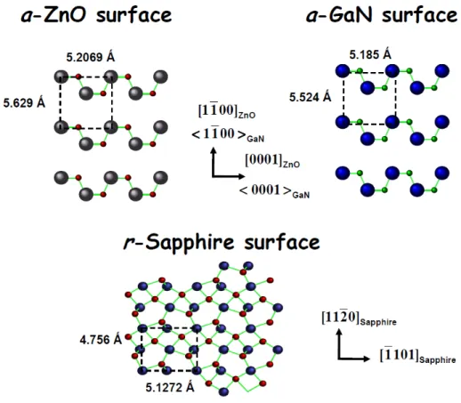
Different from the polar case, the a-plane ZnO layer has a misfit anisotropy with the substrate.22,24 As illustrated in Figure I. 6, the lattice spacing of ZnO is cZnO = 5.206 Å along
the [0001] direction of ZnO and that of the sapphire substrate is 384
. 15 3
'sap= asap2 +csap2 =
c Å. Such a large lattice mismatch can be accommodated by
matching three ZnO (0001) planes with one sapphire
(
1101)
plane, with 1.26% misfit left. Along the [-1100] direction of ZnO, the lattice periodicities of ZnO and that of sapphire are 3aZnO =5.629Å and asap=4.756 Å, respectively, and there is a compressive lattice misfitof 18.3%. This misfit is accommodated in the form of DME, as introduced in the case of c-plane growth24.
When the III-nitrides are grown on r-plane sapphire, similar crystal matching arrangements with ZnO / sapphire have been identified.25 As shown in Figure I. 6, the epitaxial relationships between a-plane GaN and r-plane sapphire are:
(
0001)
GaN ||( )
1101sapand(
1100)
GaN ||(
1120)
sap, and the lattice misfits are accommodated ina similar form with that of ZnO and sapphire. The lattice misfit is ~ 1.13% along GaN <0001> direction and 16.1% along <1-100> direction.
[11-20]
[0001]
[1-102]
[-1101]
[1-102]
[11-20]
(a)
(b)
Figure I.6. Scheme of the atomic arrangements and lattice constants of a-plane ZnO, a-plane GaN and r-plane sapphire.
I.1.2.c.
GaN grown on ZnO
GaN has very small lattice mismatches with ZnO (-1.87% and -0.42% along [11-20] and [0001] directions, respectively). When growing GaN on ZnO, GaN follows exactly the stacking orientation of ZnO, either along polar or nonpolar directions.18,26 The epitaxial relationships are:
(
0001)
GaN ||(
0001)
ZnO,( )
1120GaN ||( )
1120 ZnO and(
1010)
GaN ||(
1010)
ZnO.I.1.3.
Strain and stress
where a0 and c0 are the relaxed lattice parameters, and a and c are the strained lattice
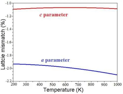
parameters. In the GaN epitaxial layer, the strain is usually generated from the lattice mismatch between the substrate and the epi-layer. For instance, when growing on c plane, a GaN film exhibits a compressive in-plane strain on sapphire, and a tensile strain on ZnO. When growing on nonpolar planes, the situation is more complicated as there are in-plane anisotropies for the lattice parameters and the thermal expansion coefficients along a (or m) and c directions, so in-plane strains are usually anisotropic.26 As illustrated in Figure I. 6, the lattice mismatches between GaN and ZnO are -1.9% and -0.4% along [1-100] and [0001] directions, respectively, while those between GaN and sapphire are 13.9% and 1.13% along [1-100] and [0001] directions, respectively.
There are two types of strains: normal strain and shear strain. Normal strains are noted as
ε
xx,ε
yy, andε
zz, representing strains along the three orthogonal directions [11-20], [1-100]and [0001], respectively. Shear strains are noted as
ε
xy,ε
yz, andε
xz, and they describe thechange of angles between the three principle directions, owing to the stress along non-principle axes. In the case of heteroepitaxy, only normal strains are present when growing on polar and nonpolar orientations. Shear strains occur when growing on semipolar planes.27
The relation between the strain and the stress obeys to the Hook’s law:
σ
ij =Cijklε
kl (I. 5)In the wurtzite system, both stress and strain vectors have six elements, and the stiffness matrix elements Cmn
(
m,n⊂[ ]
1,6)
have only five independent constants: C11, C12, C13, C33 andC44. The strain-stress relations can be expressed as:
(
)
− = xy xz yz zz yy xx xy xz yz zz yy xx C C C C C C C C C C C C Cε
ε
ε
ε
ε
ε
σ
σ
σ
σ
σ
σ
2 / 0 0 0 0 0 0 0 0 0 0 0 0 0 0 0 0 0 0 0 0 0 0 0 0 12 11 44 44 33 13 13 13 11 12 13 12 11 (I. 6)The elastic stiffness coefficients of GaN and ZnO have been measured experimentally as shown in Table I. 3: Structure C11 C12 C13 C33 C44 GaN28 wurtzite 390 145 106 398 105 InN28 wurtzite 223 115 92 224 48 AlN28 wurtzite 396 137 108 373 116 ZnO29 wurtzite 209.7 121.1 105.1 210.9 42.5
Table I.3. Elastic stiffness coefficients of nitride binaries and ZnO (GPa).
When growing GaN on the (0001) plane, there is no shear strain, and the in-plane strain is isotropic (εxx = εyy = ε//). The crystal space group does not change. The stress along
the growth direction vanishes because of the free surface, we have:
σ
zz =2C13ε
// +C33ε
zz =0 (I. 7)Then the relation between the transversal strain ε// and axial strain εzz can be expressed as:
ε
// =−vε
zz, (I. 8) where 13 33 2C C v= is Poisson’s ratio.When growing GaN on the (11-20) plane, the epitaxial layer is strained on the yz plane (cf. Fig. I. 13), and the strain is anisotropic due to the different lattice mismatches along the
y-[1-100] and the z-[0001] directions. In this case, the crystal symmetry is changed from
wurtzite C to v6 C . The stress along the growth direction satisfies: v2
I.1.4.
Defects
I.1.4.a.
point defects
Point defects mainly have two sources: native defects and impurities. There are several types of native point defects in GaN, like Ga (VGa) and N (VN) vacancies, self-interstitials
(Gai and Ni), and antisites (GaN and NGa). The presences of these native defects may act as
sources of doping, and also sources of compensation for intentional doping. These native defects usually have a high formation energy,30 which makes them difficult to form spontaneously during the growth.
Impurities are another type of point defects. The most common impurities in GaN are O, C, and Si, and they are mainly incorporated into GaN layers, usually non-intentionally, during the growth. The impurities may also influence the electronic properties of the epitaxial layer. For example, Si and O, which act as donors in GaN, can lead to a non-intentional n-type conductivity and compensate the intentional p-type doping in the epitaxial layer.
I.1.4.b.
line defects
A dislocation is a typical line defect, which can be divided into two groups: threading dislocation and misfit dislocation. For GaN, they can be generated from the coalescence of islands or relaxation processes during growth, although there is no low energy relaxation process when growing along polar orientation.31,32,33 The typical threading dislocation density of a GaN layer grown on sapphire (by MOCVD or MBE) is between 108 and 1010/ cm2.31,34 Thick GaN layers (>300µm) with a dislocation density of mid-106/cm2 can be grown by HVPE35. The surface terminations of dislocations may lead to the formation of depressions due to the surface energy and the strain energy associated with the dislocations.36 Figure I. 7 shows the scheme of a surface generated from the force balance between the surface tension and the dislocation line tension, at the termination of a dislocation. These depressions may finally result in ‘V-shape’ defects observed, for instance, in InGaN / GaN multi quantum well (MQW) structures.37 The presences of dislocations may influence the electrical and optical properties of GaN, i.e. they may act as localized non-radiative recombination centres of excitons.37
Figure I.7. Scheme of a surface depression generated at the termination of a dislocation (adapted from ref. 34).
Figure I.8. Schematic representations of (a) an edge dislocation and (b) a screw dislocation.
I.1.4.c.
planar defects
The most commonly observed planar defects in wurtzite GaN are stacking faults (SFs) and inversion domain boundaries (IDBs). Basal plane stacking faults (BSFs) correspond to the disordered stacking sequence of a crystal in the (0001) plane of GaN, while prismatic stacking faults (PSFs) refer to stacking faults in prism planes. In a perfect wurtzite crystal, the stacking sequence is ABABABAB, as show in Figure I. 9 (a) and (c). The stacking sequence is ABCABCABC for a zinc blende structure (Figure I. 9 (b) and (d)). For type I BSF, the stacking sequence is switched to ABABCBCB, as all the A sites are replaced by the C sites above the fault plane. A type II fault represents a stacking sequence of ABABCACA, and an extrinsic fault is characterized by a stacking sequence of ABABCABAB.
Figure I.9. Schematic representations of A, B, C sites in (a) wurtzite and (b) zinc blende structure; (c) and (d) shows the projection on the c plane (0001) (adapted from ref. 38).
An IDB represents a fault plane which acts as an inversion centre for domains with different anion-cation bond polarity. In GaN, IDBs having (10-10), (10-11), (10-12) and (0001) faults planes have been observed.39,40 Figure I. 10 shows an atomic model of IDB in the (11-20) plane. The dotted line indicates the bond centre site where the inversion happens. IDBs can be evidenced by the asymmetry in convergent beam electron diffraction (CEBD) patterns containing the (0002) and (000-2) reflections.40
Figure I.10. Atomic model of an IDB in (10-10) plane (adapted from ref. 41).
I.2.
GaN electronic band structure
I.2.1.
Band structure near
Γ
point
GaN, like other III-nitride materials and ZnO, is a direct band gap semiconductor. Figure I. 11 shows the band structure of GaN in the first Brillouin zone. The conduction band minimum and valence band maximum locate at the center of the Brillouin zone, which is called the Γ point. The band gap Eg represents the energy difference between the conduction
band minimum and the valence band maximum. The band gap energy decreases with the increasing temperature, and this behaviour is described by the Varshni equation:
( )
β
α
− − = T T E T Eg g 2 0 ) ( , (I. 11)( )
Figure I.11. GaN band structure in the first Brillouin zone, simulated using local approximation (dashed line) and quasi-particle self-consistent (solid line) approaches (adapted from ref. 42).
In the vicinity of the conduction band bottom, the electronic state mainly consists of the anti-bonding state of cation s state, and the energy dispersion can be expressed by a parabolic approximation model:
( )
(
)
z(
xx yy)
zz e y x e c c c c k a a m k k m E E E k E 2ε
ε
1ε
2 // 2 2 2 2 0 0 2 2 + + + + + + = + = h ⊥ h , (I. 12)Ec0 represents the original position of the conduction band minimum. The second and the
third terms represent the parabolic sharp energy dispersion in the vicinity of the conduction band bottom, where m and e⊥
//
e
m are the effective masses of the electron in the basal plane
and along the c axis of the Brillouin zone, respectively. The electron and hole effective masses of nitride binaries and ZnO are listed in Table I. 4. The last two terms correspond to the energy shift due to the residual strain: a1 and a2 are the deformation potentials along the
in-plane and out of plane directions, respectively, which are also listed in Table I. 2.
The band structure of the valence band is more complicated. There are three doubly degenerated energy levels at the top of the band, determined by the p-like bonding states. In an unstrained GaN layer, the three sub bands are the heavy hole band, the light hole band and
the spin orbit split off band, and the excitons related to these three bands are named as A, B and C excitons, respectively. The holes in each sub bands have different effective masses. The effective masses corresponding to the three sub bands are defined as mA, mB and mC, and
listed in Table I. 4. One important part of this thesis focuses on GaN layers grown along the nonpolar (11-20) orientation. In this case, possible in-plane anisotropic strains may lead to a mixing of the sub bands.43 Therefore, the excitons corresponding to the transition between the conduction band and the three sub bands are denoted as X1, X2 and X3 excitons (Figure I. 12),
from the lowest to the highest transition energy, respectively.
Figure I.12. Scheme of the sub valence bands and the associated exitonic transitions with the conduction band. ⊥ e m m e// ⊥ A m m B⊥ ⊥ C m m //A // B m m aC// 1(eV) 6 a2(eV)6 GaN44 0.18 0.20 1.65 0.15 1.10 1.10 1.10 0.15 -4.9 -11.3 ZnO45 0.21 0.23 0.54 0.55 1.12 2.74 3.03 0.27 AlN44 0.25 0.33 3.68 6.33 0.25 0.25 3.68 3.68 -3.4 -11.8 InN46 0.10 0.11 1.61 0.11 1.67 1.67 1.67 0.10 -3.5 -3.5
Hamiltonian.44,48,49 In this method, the subband states and energies can be deduced from the eigen states and eigen values of Bir- Pikus Hamiltonian matrix:
∆ ∆ − ∆ − − ∆ − = F I K G I K I H I H K H G K H F k H 0 0 0 0 0 0 0 0 0 0 0 0 0 0 ) ( * * * * * *
λ
λ
r , (I. 13) where(
)
(
)
(
)
(
)
3 2 2 2 4 3 2 4 2 3 2 1 2 2 2 1 3 5 2 5 6 7 6 6 7 6 2 1 2 1 2 , , , , 2 , , , 2 , , , , , ∆ = ∆ + = + = + = + − = + + + + = + + + + = ∆ = ∆ + = + − = + + = + + ∆ − ∆ = + + ∆ + ∆ = ⊥ + + + ⊥ ⊥ + + + + + + + + y x y x yz xz z xy yy xx yy xx zz z yy xx zz z z z z z k k k ik k k i i D D k A k A D D k A k A D k A K D k A k k A i I D k A k k A i H G Fε
ε
ε
ε
ε
ε
ε
ε
ε
ε
θ
ε
ε
ε
λ
ε
ε
ε
θ
λ
θ
λ
The parameters Di (i=1 to 6) are the deformation potentials of the valence band. Two groups
of GaN deformation potentials have been proposed in literature, which are listed in Table I. 5. Deformation
parameters
Ref.49 (eV) Ref. 50 (eV) D1 -41.4 -38 D2 -33.3 -33.3 D3 8.2 4.9 D4 -4.1 -5 D5 -4.7 -2.8 D6 -7.5 -3.1
Table I.5. Deformation potentials of the GaN valence band proposed by Ghosh et al.49 and Ishii et al.50.
Aj (j =1 to 7) are equivalent to the Luttinger parameters and determine the hole effective
masses.51
ε
mn and km (m, n =x, y, z) are the strain and wave vector components. ∆1 = ∆cr, ∆2 = ∆3 = ∆so / 3, where ∆cr is the crystal field splitting energy, and ∆so is the spin orbit
(
)
(
)
(
)
(
)
, . 2 1 , , 2 1 , , , , , , 2 1 , , 2 1 6 5 4 3 2 1 ↓ − = ↑ − = ↓ = ↑ = ↓ + = ↑ + = iY X u iY X u Z u Z u iY X u iY X u (I. 14)where X , Y and Z are the wavefunctions of the three p-like states, with orbital orientations along x, y and z directions, respectively (illustrated in Fig. I. 13). ↑ and ↓ represent the wave functions of spin up and spin down states. The eigen energies and eigen states can be deduced by diagonalizing the Bir- Pikus Hamiltonian matrix. It gives the valence energies Evj(j=X1, X2, X3) and wave functions
∑
= = Ψ 6 1 i i i j
VB au of the sub bands.
Figure I.13. Coordinate system (xyz) used in this section (adapted from ref. 52).
The oscillator strength of the transition between the conduction band and valence band is proportional to the square modulus of the transition matrix elements:
2 j VB i CB j i p f ∝ Ψ Ψ , (I. 16)
where fi (i=x,y,z) represents the oscillator strength when the electric field E is along i
direction, and pi is the momentum operator along this direction. ΨCB is the conduction band
wave function, which has a spherical shape and can be simplified as S . The valence band wave function
∑
= = Ψ 6 1 i i i jVB au is composed of the three p-like states X , Y and Z . The
selection rules are deduced from the wave function symmetry in the matrix element operation:
// I Y p S X p
S x = y = and S pz Z =I⊥; otherwise, S pi j =0 if i≠ j. At zero strain state, the two topmost sub valence bands only have components from X and Y states:
(
X ±iY)
b2 1
, therefore the emission from X1 and X2 exciton recombination is isotropic in
the basal plane. The X3 emission is polarized along the c-axis, because the corresponding
valence band wave function is constructed by the Zb states.52
I.2.2.
Shallow and deep levels in the band gap
The doping of semiconductors is one of the fundamental steps towards the fabrication of optoelectronic devices. N- and p-type GaN layers are desired when growing nitride based LED and laser diode (LD) structures. An undoped GaN layer usually exhibits an n-type conductive behaviour, due to the unintentional doping of impurities such as O and Si.30 Actually, there are two sources of GaN n-doping: native defects and impurities. Native defects, mainly referring to N-vacancy (VN), may act as a shallow donor. However, the high formation
energy of VN in n-GaN makes it is difficult to occur in significant concentrations.54 Si and O
are the two principal impurities which are responsible for GaN n-type doping: Si is often used for intentional doping and O is the main source of non intentional doping. Si usually exists in GaN by substituting a Ga site and has an ionization energy of 25 meV.54 O may occupy a N site and act as a shallow donor of GaN, with an ionization energy of 26 meV.54
The p-type doping of GaN is more difficult. Mg has become the dopant of choice to obtain p-GaN layers. Mg may occupy several sites in GaN, including the replacement of a Ga site (MgGa), an antisite (MgN) and an interstitial site (Mgi). Usually, MgGa has a lower
formation energy than MgN and Mgi, so the MgGa configuration is favoured in energy.54 The
ionization energy of the Mg acceptor is determined experimentally to be between 200 - 250 meV in GaN.55,56,57 This high activation energy results in a low hole concentration compared with the Mg concentration. Currently, the typical hole concentration achieved in p-GaN layers for the fabrication of LEDs is in the order of ~ 1018 / cm3.58
The transition of an electron from the donor level to the acceptor level may lead to the donor acceptor pair (DAP) emission in the photoluminescence spectrum of GaN (see Figure I. 14). The DAP emission energy can be calculated by:
(
)
r e E E E hvDAP g D Aπε
4 2 + + − = , (I. 17)where ED and EA represent the ionization energies of donors and acceptors, respectively. The
last term corresponds to the Columb interaction between the donor and acceptor pair, and r is the distance between the donor and the acceptor.
experimentally by Yi and Wessels.61 The transition between a shallow donor level and this deep level (Figure I. 14) has been generally accepted as the origin of yellow luminescence (~ 2.25 eV at room temperature), which has been observed in GaN layers grown by several techniques.59,62
The complex between the MgGa acceptor and the N vacancy may introduce a deep
donor level in GaN (MgGaVN), which is about 0.4 eV below the conduction band. The blue
band observed in GaN PL spectrum (~ 2.8 eV) has been attributed to the transition between this deep donor level and the acceptor level.63
I.3.
III-Nitride heterostructures and applications
I.3.1.
Nitride bandgap engineering
There has been an increasing interest in fabricating opto-electronic devices based on III-nitrides during the last two decades. One important reason is that the band gap of nitrides and their alloys cover a broad range from 0.7 to 6.0 eV. In addition, the wurtzite phases of nitrides are direct band gap materials. These unique optical properties make nitrides suitable for a large range of opto-electronic applications, such as LEDs, LDs and photo-detectors operating in the UV-visible range.64,65
Figure I.15. Band gap energies, at room temperature of wurtzite III-nitrides as a function of the lattice constant a.
Figure I.15 shows the band gap energies of nitride binaries and their lattice constant values a. GaN and AlN have closer lattice constants than InN. The band gap energies of nitrides have been summarized by Vurgaftman and Meyer6 and are listed in Table I. 6.
material InN GaN AlN structure wurtzite wurtzite wurtzite band gap (eV) 0.78 3.51 6.0
Table I.6. Band gap energies of nitride binaries at 0 K.
A nitride based alloy with a band gap energy in the range of 0.7-6.0 eV can be achieved by adjusting the content of InN, GaN and AlN. The band gap energy of an A1-xBxN
alloy can be calculated approximately by:
E
( ) (
x x)
E xEgBN bx(
x)
ANg
g = 1− + − 1− , (I. 18)
where b is the bowing parameter. Table I. 7 lists the bowing parameters of different nitride alloys summarized by Vurgaftman and Meyer:6
Alloy AlGaN GaInN AlInN
b (eV) 0.7 1.4 2.5
Table I.7. Bowing parameters of AlGaN, GaInN and AlInN alloys.
I.3.2.
Polar heterostructures
There is a strong polarization field along the c axis ([0001]) in a wurtzite crystal. The polarization field in nitrides consists of spontaneous and piezoelectric polarization. The total polarization can be obtained from the sum of spontaneous and piezoelectric polarizations: