DESIGN PORT AND OPTIMIZATION OF A HIGH-SPEED
SAR ADC
COMPARATOR
FROM
65NM
TO
0.11pM
by
Nora Iordanova Micheva
B.S. Electrical Engineering and Computer Science,
MASSACHUSETTS INSTITUTE
OF TECHqOLOGY
JUN 2 1 2011
MIT, 2010
LIBRARIES
Submitted to the Department of Electrical Engineering and Computer Science in Partial Fulfillment of the Requirements for the
Degree of Master of Engineering in Electrical Engineering and Computer Science at the Massachusetts Institute of Technology
ARCHNES
May 2011Copyright Massachusetts Institute of Technology. All rights reserved.
The author hereby grants to MIT permission to reproduce and to distribute publicly paper and electronic copies of this thesis document in whole and in part in any
medium now known or hereafter created.
Author:
Department of Electrical Engineering and Computer Science May 17, 2011 Certified by:
Certified by:
Accepted by:
Charles G. Sodini, LeBel Professor of Electrical Engineering Thesis Supervisor
Doris Lin, Design Engineer, Analog Devices Inc. Thesis Co-Supervisor
Dr. Christopher
J.
Terman Chairman, Masters of Engineering Thesis CommitteeDESIGN PORT AND OPTIMIZATION OF A HIGH-SPEED
SAR ADC
COMPARATOR
FROM
65NM
TO
0.11IM
by
Nora Micheva
Submitted to the Department of Electrical Engineering and Computer Science May 15, 2011
In Partial Fulfillment of the Requirements for the Degree of Master of Engineering in Electrical Engineering and Computer Science
ABSTRACT
As the world continues to do more and more of its signal processing digitally, there is an ever increasing need for high speed high precision signal processors in consumer applications such as digital photography. Technological progress in CMOS fabrication has allowed chips to be made on nano scale processes, but this still comes at a steep price. Especially in chips for which analog components are a priority over digital components, some of the benefits of using nano scale processes diminish, such as smaller area. In these cases, it is worth investigating whether the same performance can be achieved with larger feature size, and therefore, cheaper processes.
To that end, a three-stage comparator circuit for use in a digital camera SAR
ADC has been ported from its original 65nm process to a 0.11ptm process. Its
design has been analyzed and performance presented here. Additionally, an alternative latch-only architecture for the comparator has been designed and analyzed. In 0.11pm the three-stage comparator operates at the same speed,
13% lower RMS noise contributing 0.9 bits difference, and 11% higher
power than the original in 65nm. More noteworthy, the 0.11pm latch-only comparator operates at 40% higher speed, equivalent noise, and 72% lower power.
ACKNOWLEDGMENTS
My thesis was sponsored by MIT and Analog Devices, Inc. through the VI-A program,
which allowed me the opportunity to work on a real-world industry project while at the same time obtaining a Master's degree. I would like to especially thank my advisor at ADI, Doris Lin. She was there for me every step of the way, providing patient guidance and support when I needed it the most. I think she is a great mentor and I will remember my time at ADI fondly.
I would also like to thank my faculty advisor at MIT, Professor Charles Sodini. He
provided guidance to me even before I began working on my M.Eng., and offered to be my supervisor despite his hectic schedule. I am thankful for his advice on which direction to take in my thesis, and his insistence on quality work. I will take these lessons with me in my career going forth.
At ADI I would first like to thank Ron Kapusta, whose work this thesis is based on, and who first recruited me to the group. His intuitive explanations always made the difficult seem easy to me. I would also like to thank the design engineers who always welcomed my questions no matter how silly they were: Henry Zhu, Junhua Shen, Steve Decker, Dave Roberts, Mark Sayuk, and Katsu Nakamura. I would like to thank the lunch cohort (Mitushi, Yero, Neal, Ned, Jason, Vivek, Paul) for making me really feel like a part of the team, and Mark Robinson for his cheerful conversations with me.
While he wasn't on the team, I'd like to give special thanks to Benjamin Walker, the VI-A representative from ADI. He made me feel at home from day one, and always took special time to check up on me. I am grateful for all the new EE concepts I learned from him during our weekly meetings.
At MIT, I would like to thank Anne Hunter for having her door always open to me, no matter what trouble I had to bring to her. She had faith in me four years ago when I decided to become course 6 and was nervous about all the catching up I had to do, and she's still there for me now. I'd also like to thank Professor Joel Schindall, my department adviser and director in the Gordon Program, for being a mentor to me all this time in course 6 and in
GEL, in which I learned so much about what I'm really capable of.
Finally, I would like to thank my mom, dad, Peri, and Simon for loving and supporting me through it all. MIT has been quite a journey, and I am certain that I couldn't have done it without them. My mom and dad for trusting that I could do anything I put my mind to even when I didn't, Peri for being the best little sister I could ever dream to have, and Simon for loving me unconditionally and taking in stride everything this journey took
us to.
TABLE OF CONTENTS
Chapter 1: Introduction... 6
1.1 M otivation... 6
1.2 Fundam entals and Basics of Operation ... 8
1.2.1 A peek into SAR A DCs ... 8
1.2.2 Com parator Design Fundam entals ... 10
1.3 State of the A rt... 12
1.4 Specifications of Interest... 13
Chapter 2: Characterization of 65nm vs 0.11um Process...15
2.1 Transconductance ... 16
2.2 Output Resistance...18
2.3 Parasitic Capacitances... 20
Chapter 3: 65nm Com parator Topology A nalysis...21
3.1 Stage 1: Integrator... 21
3.2 Stage 2: Pream plifier ... 26
3.3 Stage 3: Latch...30
Chapter 4: Design Port... 32
4.1 Design Port + Perform ance of Stage 1... 34
4.2 Design Port of Stage 2 and Performance of Stages 1 + 2... 37
4.3 Design Port of Stage 3 and Performance of All Stages Together ... 39
4.4 Results... 39
Chapter 5:N ew Architecture ... 41
Overall Results...42
Chapter 6: Conclusion and Future W ork ... 43
Chapter 7: Appendix... 44
7.1 Testing for Speed/Accuracy: Hysteresis Analysis... 44
7.2 N oise A nalysis: SpectreRF...447
TABLE OF FIGURES
Figure 1: Example of a current 12-bit CCD Signal Processor [3] on the market by Analog Devices.
The ADC is highlighted in with a star... 6
Figure 2: SAR ADC Architecture [2]... 8
Figure 3: A representative 4-bit SAR ADC Architecture (adapted from [2])... 9
Figure 4: Close-up of 4-bit SAR function given VSH=0.6V... 10
Figu re 5 : C om p arator... 1 0 Figu re 6: D ynam ic Latch [7]...11
Figure 7: Small-signal MOSFET model...15
Figure 8: Transconductance versus current for the four devices; W=1pm for all, L= minimum length; ... 1 6 Figure 9: Ron versus width for 0.11 tm NMOS device... 19
F igu re 1 0: 6 5 n m Stag e 1...2 1 Figure 11: Model of input and cascode transistor on one side of the first stage, including each noise cu rre n t ... c2 5 F igu re 12: 6 5 n m Stage 2 ... 2 6 Figure 13: Model of Stage 2's cross-coupled devices...27
Figure 14: Stage 2 Close-up of Cross-coupled loads... 29
F igu re 1 5: 6 5 n m Stage 3 ... 3 0 Figure 16: 0.11 m Comparator...32
Figure 17: Final Dimensions of 0.11ptm Stage 1... 34
Figure 18: Close-up of Switches in 0.11 m Stage ... 35
Figure 19: Close-up of Stage 1 input-pair in 0.11tm... 35
Figure 20: Resistances looking up and down between the input and cascode devices of Stage 1...36
Figure 21: Final Dimensions of Stage 2 in 0.11um... 37
F igu re 2 2: Stag e 3 ... 3 9 Figure 23: New Latch-only Architecture...41
Figure 24: Implementation of Latch-Only Architecture [8]... 41
Figure 25: 640pV/-20V Hysteresis test for three comparator types ... 45
Figure 26: 20mV/-160[pV Hysteresis test for three comparator types ... 46
Figure 27: SpectreRF pss analysis ... 47
CHAPTER
1:
INTRODUCTION
1.1
MOTIVATION
Nano scale CMOS technologies provide many benefits in the implementation of today's highly digital circuits, especially in consumer electronics. Digital circuitry follows
Moore's law [1] in that moving to a smaller feature size process means more digital components can fit in the same area. Also, smaller devices offer higher gate speed at lower power dissipation digital circuitry. Analog circuits, however, do not necessarily shrink as many designs do not use or allow for minimum length devices. Therefore, in chips in which analog components are more emphasized, some of the benefits of smaller scale technologies such as a reduced chip area are no longer as relevant, and are therefore offset by drawbacks such as higher expense. This makes it worthwhile to investigate implementation of the circuits in larger feature size processes.
The setting of this thesis is the field of high-speed high-precision signal processors for digital camera and camcorder applications. One of the major components of these signal
EtR weF processors is the high-speed ADC
AD9920A
-0 B VoEr (analog-to-digital converter, see
CCDIN CoS VGA OUT
=6d
1T42d star outline in Fig. 1). Several
3V INPUT D CLK
IVOUTPUT REG different types of ADC's are
INTERNAL CLOCKS
AG ' ...f 4#
+commonly
used
in
signal
VHTOVORIZONTAL
DRIVERS GENERATOR SL
H1TERONS ECK processing applications including
VIA TO VS (3-LEVEL) 19 X1 OX SOATA
V. TO VD6 11G SY~ NC Hflash, pipeline, and Successive
Approximation Register (SAR) apO?, GPOS
[2]. Flash ADCs are fast parallel
Figure .: Example of' a current 12-bit CCg Signal Processor 31 on the market by Analog Devices. The ADC is highlighted in with a star.
converters but they have a drawback in that for an N-bit flash ADC, 2N-1 comparators are necessary, thus power and area becomes an issue. Pipeline ADCs are very good for high-speed applications, but their power consumption is often an issue [2]. While the high-high-speed
ADC of choice for the Digital Imaging Group has traditionally been a pipeline ADC, with its
transition from 0.18[im to a 65nm CMOS fabrication process, the group began investigating the use of SAR ADCs instead. SAR ADCs tend to consume less power than pipelined ADCs at the cost of speed, but due to the inherent increase in gate speed of the 65nm process node, this trade-off of speed for power was able to be circumvented, and the same spec was achieved by the group. Also, unlike pipeline ADCs, SAR ADCs do not require an amplifier and are thus better suited for smaller process devices with intrinsically lower gain. For this reason, the group decided to use the SAR architecture for its 65nm ADC.
This thesis describes the design port of a comparator for a SAR ADC in digital still camera and camcorder applications, from the 65nm to 0.11pm process node. The two processes have similar characteristics and both operate off a 1.2V supply. Hence, 0.11im seems like a cheaper alternative to 65nm for chips in which there is less emphasis on digital circuitry, because the area taken by the analog components will be roughly the same. For this reason, porting strategies that maintain the 65nm comparator's performance while moving to the 0.11ptm process are investigated here. Furthermore, a different architecture from the one used in 65nm is explored and its relative performance is presented.
The group has never utilized a 0.11ptm process before, so this will be the company's first investigation to transition the design of their high speed SAR ADC comparator from 65nm to 0.11m. The SAR ADC is a 14-bit converter with two redundant bit decisions, for a total of 16 bit decisions. The first 5 MSBs (most significant bits) are decided by an auxiliary flash ADC, leaving 11 decisions for the comparator to arbitrate.
The comparator designed by Analog Devices comprised of three stages: two preamplifier stages, followed by a dynamic latch. While the dynamic latch can make comparator decisions on its own, the preamplifiers increase the signal to overcome offset in the comparator. The preamplifiers also shield the input signal from charge kickback in the latch, defined the charge that is "kicked back" to the inputs through Cgd of the input pairs when the latch regenerates. While this doesn't have negative repercussions for all input signals, the inputs in this case come from a capacitive DAC used for sampling that is sensitive to this charge kickback.
1.2
FUNDAMENTALS AND BASICS OF OPERATION
1.2.1 A PEEK INTO SAR ADCs
A SAR ADC uses a successive approximation binary search algorithm to get a digital
representation of an analog input signal. Fig. 2 shows a simplified representation of a SAR
ADC, whose main components are a Track/Hold stage, a SAR logic/register stage, an N-bit
digital to analog converter (DAC), and a comparator.
Analog in - Track /Hold -N + Comparator
vnAC
V REF N-bit DAC
DigitaI data out
N-bit (serial or parallel)
Register
SAR Logic
Each conversion period consists of two phases: in the first one, the analog signal is tracked and held, and in the second one, the digital output bits are resolved by the SAR logic. Fig. 3 is an example diagram of a four bit SAR ADC using a feedback capacitive DAC.
VINH
v.
--
S/H
T 0 T 0 Reset switchbfbWb
0th
b
3bzbi
b
Successive Approximation Logic
Figure 3: A representative 4-bit SAR ADC Architecture (adapted from [21)
Let us take an example with the held value being VSH=0.6V and VREF=1V. After
resetting the DAC voltage VDAC=OV, the most significant bit (MSB), b3, is instantiated as 1. This connects the capacitor for the MSB to VREF and makes the DAC voltage to be fed into the comparator to become 0.5*VREF, or O.5V. At the comparator level, this is compared to 0.6V and since it is higher, the comparator outputs a logic '1', which is translated through the successive approximation logic to set b3 to 1 for the remainder of the translation. If the sampled voltage were lower than O.5V, the Reset Switch would be used to reset the capacitors and turn b3 to 0 for the remainder of the cycle. A similar process is used for the remainder of the bits, eventually converging VDAC to VSH. The figure below shows this
VSH=
0.60V
1.00 0.75-m~ 0.50-00 Timeb,=1
b
2=0b=0
b,=1
Figure 4: Close-up of 4-bit SAR function given VSH=0.6V
1.2.2 COMPARATOR DESIGN FUNDAMENTALS
High speed comparators are critical in making a high speed SAR ADC, because they are one of the main bottlenecks in the overall speed of the ADC. The comparators used in this application take the difference between V+ and V- and if it is positive (i.e. V+ is larger)
VS they output a logic '1', otherwise they output a logic '0'. The speed,
V + or a response time in a comparator is defined as the delay between
V_ -the time the differential input passes the comparator threshold
vs_
voltage and the time the output exceeds the input logic level of theFigure 5: Comparator subsequent stage [4].
One of the simplest forms of a comparator is a two stage compensated op-amp. Compensation of an op-amp often involves the separation of the poles of an op-amp by lowering one pole through the addition of a large capacitor at the output [4]. This form of compensation greatly decreases the speed of op-amps and makes them undesirable for high-speed applications. Even in the uncompensated case, however, the response time is still significantly slow due to other parasitic capacitances, and making this type of
A significantly more popular approach to making
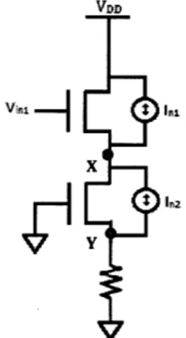
a high speed comparator involves multiple stages: one or more high-speed differential pre-amplifier stages often followed by a dynamic latch stage [4]. The purpose of the pre-amplifier stages is to cancel offset and amplify the input voltages to an extent that the input offset voltage becomes negligible. The dynamic latch (shown in Fig. 6) in turn uses strong positive feedback when the clock is high and the input is being sampled to obtain high gain (albeit non-linear) and output a logic '1' or '0' very quickly.
Vdd
110
S3
Figure 6: Dynamic Latch [7]
Another design technique to make the comparator even faster involves replacing the active loads (e.g. diode connected loads) in the pre-amplifier stages with resistive loads [4]. This speed increase is due to the limit on the response time by the parasitic capacitances of the load devices. One drawback to this resistive load (other than more power being consumed), however, is that the voltage drop across the resistors can vary significantly with process variations, such as resistor mismatch.
While the SAR ADC to be investigated is 14-bit, 5 of those bits will go through a flash
ADC, leaving only 9 bits (plus the two redundant bits mentioned in the previous chapter) to
the SAR ADC. The SAR ADC therefore only needs to be mid resolution, and design techniques similar to those described here will be useful.
1.3
STATE
OF THE
ART
One of the earlier comparator architectures was designed by McCarroll, Sodini, and Lee in 1988 [7]. Pre-amplifier stages were used on Vi. (which is to be compared to Vref),
after which the amplified (Vi. - Vref) was put through a dynamic latch. For the pre-amplifier
stages, three configurations were investigated depending on the required output voltage (that would be the input to the dynamic latch): a single stage amplifier, a single stage amplifier with a source follower, and a two stage amplifier with a source follower. The response time was calculated for each and was plotted as a function of the output voltage. For an 8 bit ADC it was found that the one stage pre-amplifier plus a source follower was the optimum configuration. Architectures similar to this one are investigated in detail in this thesis.
More recent papers on SAR ADCs exhibit successful implementations of comparators using only the latch stage [8], or using a single preamp stage and latch stage [9]. An alternative implementation of the 65nm design based on one of these papers will be discussed further in the thesis. It is also useful to take a step back and compare resolution and speed specifications achieved in recent literature, along with the choice of process to be used. The table below compares resolution, speed, and process used in seven recent (2007 on) publications of SAR ADCs. They are organized in order of increasing resolution. Several trends can be seen from these papers. First, speed decreases significantly when the resolution transitions from mid-range (10 bit) to high-range (12 bit and beyond). This follows intuitively because it takes longer to achieve higher-resolution conversion. Another trend can be seen when comparing the two 10 bit SAR ADCs: higher speed can be obtained
by using a smaller feature size process such as the one we see below from 90nm to 65nm,
something we are trying to circumvent in this thesis (i.e. getting same speed even with a larger process size).
[17, 00 [8,g 00 [18], 201 [19],: 2010Ae [2 ] 2009.. ..
1.4
SPECIFICATIONS OF INTEREST
The three main specifications that this thesis will focus on are speed, noise, and power. The area of the comparator is only about 4% of the total ADC area, and a small area increase from going to 0.11pm will be negligible. Therefore, it wasn't a specification of focus in the thesis (through hand-calculations the 0.11pm comparator area was later estimated to be minimally different from the 65nm comparator area). Also, while it is not of special focus in this thesis, it should be noted that offset must be overcome to get the right bit decision.
The speed, or sample clock rate specification of the 65nm ADC is 80MHz at peak performance, allowing for integration with the 74.24MHz standard for high definition digital video (includes resolutions such as 720p60 and 1080i60) [14]. However, because this particular SAR was designed by the group to be self-timed, there isn't a specific time set for the comparator to finish making a decision, as long as the overall SAR clock rate is met.
Thus in this thesis, instead of keeping to a specific value the 65nm comparator's decision time will be used as a speed benchmark.
In order to match the 65nm comparator noise, the specification here has been set to 71uV rms of input referred noise. Noise in a comparator is not as straightforward to model and quantify as in most linear circuits because of the transient nature of a comparator's operation, and thus periodic noise has been measured using the "Spectre RF" simulation program [15].
The power dissipation specification is also determined by comparison to the one consumed in 65nm, and has been set to 5.4mW. Power is calculated by measuring the average current during operation and multiplying by rail-to-rail voltage, in this case 1.2V.
CHAPTER
2:
CHARACTERIZATION OF 65NM
VERSUS
0.11pM
PROCESS
If certain trends in the MOS devices in 65 nm and 0.11 pm processes are known, we
can exploit any benefits of 0.11 pm to obtain better performance when moving to this new process. If there are no benefits, we can at least be aware of the challenges to come. This thesis focuses on the following MOS parameters: transconductance (gm), switch on-resistance (Ron), and parasitic capacitance (Cgs,Cgd).
The transconductance is closely related to the
small signal gain of an amplifier: gm*rout (shown in +
Fig. 7). Therefore, higher gm tends to point to a steady-state higher gain in an amplifier of the same
dimensions. Of course, in applications involving Figure 7: Small-signal MOSFET model
reset switches, speed (versus gain) is of greater importance, and in this case a low on-resistance is desired. Parasitic capacitances can limit the speed at which a decision is made (due to 1/RC time constants) so the smaller they are the better.
2.1
TRANSCONDUCTANCE
.01-65nm NMOS a O11pm 1IMOS .001M
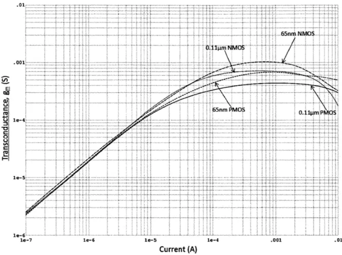
1I-7 1-5 1-4 001 .01 Current (A)Figure 8: Transconductance versus curent for the four devices; W=Ism for all, L= minimum length;
Above is a plot of gm per width versus drain current per width of four transistors: 65nm NMOS, 65nm PMOS, 0.11m NMOS, and 0.11ptm PMOS. The length is the minimum allowed by each process (0.06pim for 65nm and 0.12ptm for 0.11ptm). There are two regions to be noted in the plot: weak and strong inversion. Weak inversion corresponds to the region with lower current (roughly less than 2e-5A), in which the MOSFET acts much like a BJT in that its transconductance varies linearly with current (gm-I/Vth). During the period of weak inversion, the 65nm NMOS has the highest transconductance, although they are all quite similar. Later, once the slope of gm becomes quadratic instead of linear (varies as the square root of current here), the transistor is operating in strong inversion. At currents
above 1mA, the transistor comes out of saturation and the transconductance can no longer keep increasing due to velocity saturation (however, we are not operating in this region so it is of no concern here). In the region of strong inversion, two trends can be seen:
a) 65nm devices on average have a higher transconductance given a certain drain current than 0.11ptm devices (e.g. for 100A drain current, 65nm
NMOS gm is 17% higher than 0.11m NMOS gm).
b) PMOS devices tend to have a lower transconductance than NMOS devices.
However, due to higher gm for a given current, some of the transistors in the comparator, such as the input pair in stage 1, were biased in weak inversion. Therefore it is useful to see what the transconductance is in weak inversion (zooming into the above plot into gm for smaller bias currents) in each of the four devices. The table below shows gm/W for a 1 pA bias current (region of weak inversion).
Tran. sconductan per Width
These results have several implications for the comparator design port. First, the general trends are the same as in strong inversion, i.e. 65nm has higher trasconductance than 0.11tm, and PMOS has lower transconductance than NMOS. Why is this important? When ported to 0.11m, the gm will decrease (given the same W), and a higher width will be necessary to keep it the same. For instance, stage 1 of the comparator has PMOS input transistors, so the gm of the input pair will decrease. Taking a look at the table above, we see
that gm for 65nm PMOS is actually equal (in this case, otherwise very similar) to that of 0.11pm NMOS. This means that if we were to change the inputs to NMOS, this problem would be alleviated. The architecture in this case required a common-mode voltage of 0.25V for the inputs and thus PMOS inputs were required, but this may be something that can be changed in the future to provide a higher gm. While this difference doesn't seem so great in the table above (0.02 mS versus 0.019 mS), these values correspond to a transconductance for a unit width, so with input devices of width 576 gm biased at 3 gA, the difference in gm becomes 1.2 mS (23 mS versus 21.8 mS). While this is still a small difference, it may prove important in certain applications.
2.2
ON-RESISTANCE
The original comparator contains several reset switches and it is critical that these switches fully turn on to properly reset the comparator after each decision. Hence another parameter to consider when moving to 0.11 pm is the on-resistance of a MOS device. The smaller the on-resistance (Ron) of switch is, the closer to ideal that switch is considered to be.
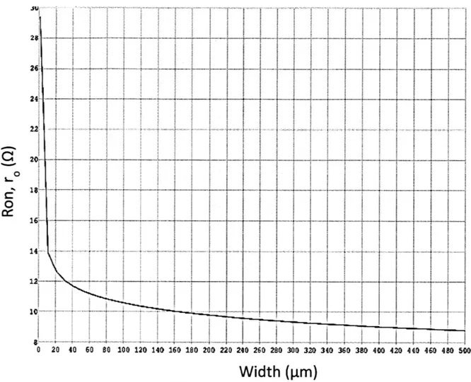
In general, as W increases Ron decreases, while as L increases Ron increases. This trend can be seen by taking the case where W or L is doubled. When W is doubled, the transistor can be thought to be in parallel with itself (while it is in series with itself when L is doubled). This means that Ron is also in parallel with itself (R = 0.5Ron) in the case of 2W, and in series with itself (R=2Ron). Fig. 9 gives one example of this trend: Ron versus width for an NMOS device in 0.11 pm, confirming the trend that Ron decreases with increased width.
12C - --- t--- - ...t... i... - - 4 ...4 -4- - ...--.
22t
S 14'
0 20 40 60 80 100 120 140 160 180 200 220 240 260 280 300 320 340 360 380 400 420 440 460 480 500
Width (pm)
Figure 9: Ron versus width for 0.1 1prn NMOS deviceThe 0.11ptm process switches have higher Ron resistance because minimum L was now increased (keeping W the same). While the case more often involves changing both W and L so these results cannot be used directly, we will be able to calculate the width required in O.11m to achieve the same Ron. This comes out to keeping the W/L ratio roughly the same: at W= 1pm, Ron was 0.7ME for 65nm NMOS (L=60nm), while it was 1.6 Mfl for 0.11 gm (L=0.12 pm). This corresponds to a factor of 2.2 increase in Ron for a factor of 2 decrease in W/L.
2.3
PARASITIC CAPACITANCES
In MOSFETs, parasitic capacitances exist between the gate, source, drain, and bulk terminals. The ones of highest magnitude are most often Cgs and Cgd, and they will be of focus here. The reason for concern when dealing with high speed circuits is that these
1
capacitances introduce more RC time constants (see equation) and21rf,
slow the circuits down.The following table shows Cgs and Cgd for the four types of devices in saturation, each with W=l m and minimum length (0.06ptm or 0.12[im):
65nm NOS 65m PMO 0.11m NMO 0.11m PMO
While the parasitic capacitances are almost identical for W=lpm, it is important to note the percentage difference in Cgs: 28% increase for NMOS and 7% for PMOS. This means that especially for NMOS devices, the change in gate capacitance will be significant. For the purposes of the thesis, this implies that we will need to be aware of this difference and make sure the NMOS devices (such as the reset switches) are as small as possible to limit speed decrease in the comparator.
CHAPTER
3:
65NM COMPARATOR TOPOLOGY
ANALYSIS
This chapter will analyze the comparator design provided by Analog Devices in 65nm. The comparator has three stages. The first two stages serve as preamplifiers and the final stage is a latch. Once basic operation and the limiting factors to speed, power and noise are known, they can be used in optimizing the design port to 0.11pm for maximum performance.
3.1STAGE1:INTEGRATOR
AVDO s=54 rn p12 vps mp 11 V=00 mpss-75 illad3 16 4 3.s-12
3=19
s12
p4 snlpe inps AVSAViS E AVS 3-30 mfd 1 Vipi DZ-P-91qraLb-bs. vns D A AvnFiu3 AVDDn PPLY PPL
vns - AVAV33
Basic Topology and Function
The first stage of the comparator is a differential amplifier that can be seen as acting as an integrator because the settling time period is significantly less than the load time constant (tint << rout *Cint ). It was chosen to work as an integrator because of its higher power efficiency in achieving the same gain target within a limited time, compared to a traditional wide-band amplifier. While the circuit does not contain an explicit capacitor on which to integrate, the input capacitance of the next stage acts as this capacitor. A cascode stage is added in to increase the output resistance of the amplifier, and therefore the DC small-signal gain gm*rout. In addition to this, a current stealing technique is applied at the source nodes of the cascode devices. This allows for less current to flow through the load, decreasing the headroom required and thereby decreasing the noise of the load. Current stealing allows for only -1/8 of the bias current to flow through the loads, and a large resistor could be used instead of active one to achieve the same gain.
Speed - gain in a given amount of time
The voltage gain was approximated to be
Gain gm,nput o tint.
Cint
To figure out why this is so, let us first look at the current flowing out of stage 1. The output current of stage 1 is determined by the transconductance of the input pair, m', times the differential input voltage:
.dv 0ut
ic = C dt 9mvin Taking the integral on both sides:
CVOne + CO = gmvindt
C. is 0 because the capacitor is initially discharged and Vin is a constant input in this case,
therefore:
9mvintint = Cvout
yin t
Because the amplifier needs to achieve a certain amount of gain to overcome offset in the latch, in order to achieve high gain for a given capacitance, we must increase either gm or tint.
In order words, the larger the capacitance on the output, the larger either the input pair transconductance or the integration time needs to be to achieve a certain gain.
Noise Analysis
The noise in the first stage integrator can be separated as coming from discrete noise sources such as the input pair, cascode devices, and resistors. The noise contribution of the input pair is greater than that of the load resistors [2], and as will be shown below, the cascode devices also contribute negligible noise. The input pair noise of an integrator is derived to be the following:
E[V2] = kT 1 4kTy
E v, = -- tint =
3 gm,in 2 9m,intin
The derivation of this noise voltage comes from realizing that the input pair of the integrator provides noise according to the noise voltage model of a MOSFET times the noise bandwidth (NBW). The noise current of an integrator is defined as:
E[in,MOSFET] = 4kTYgm,in
In order to obtain noise voltage from this current, we divide by gm,in2 (since v2 g 2 R= 2) in order to obtain:
gm,in
E[ 2 14kT y
E [Vn,MOSF ET]-4y
gm,in
Next, the noise bandwidth in an integrator has been shown to be:
NBW = 1 (NBW = noise bandwidth, tint = integration time) [12]
2 t tint
And therefore, the total noise voltage in the integrator (with a factor of 2 to take into account the differential nature of the input) becomes:
E[vn2] = (4kTy-) (2) -NBW
(
m[ 4kTy
.- . (ti)]n mtint
What design intuition does this noise equation give us? The first point to note is that the noise voltage does not depend on the integrator's capacitance. Therefore, to get maximum speed, it makes sense to use as small a capacitor as possible (thus it makes sense that no external integrating capacitor is added to the output). Second, the higher the transconductance, the lower the noise voltage power will be. Finally, integration time is inversely proportional to noise voltage, but since we have a limited total integration time
Therefore, the trade-off presented by this equation is between power and speed: how much input pair transconductance is required to achieve a certain noise given an allowed time specification.
Moving onto the cascode devices, their noise is negligible because the noise currents in these devices cycle through them instead of flowing out to the resistor to contribute to the total noise voltage (see Fig. 11).
VaD From between the two transistors at node X,
rout=l/gds can be seen looking up, and 1/ gm can be
-
In, seen looking down. Because, rout=l/gs is on averageX much larger than 1/ gm, the noise current of the input transistor, ln1, travels down through the cascode
Y
transistor, finally to go through the transistor and contribute to the overall noise voltage. In2 however,
Figure 11: Model of input and cascode
transistor on one side ofthe first stage, makes the same choice and travels up to the midpoint
including each noise current
and back down into itself. Once it travels back down through the cascode device, In2 can't go down through the load resistor because of KCL at node Y: if there is a current source In2 going up, none of it can travel through R. Instead it
must instead keep cycling around itself, and because of this, In2's effect can be considered negligible.
To summarize, the key factors to look out for in the design port of stage 1 are transconductance (maximizing it in order to minimize noise) and parasitic capacitances on the output.
3.2
STAGE
2:
PREAMPLIFIER
SUB*
Figure 12: 65nn Stage 2
Basic Topology and Function
The second stage in this comparator is a more traditional amplifier, whose function is to provide a bit more gain and to set up the bias voltage for the inputs to the 3rd stage.
Because the majority of gain is provided by the first stage, this stage does not require a cascode device. The loads are realized through cross-coupled diode loads. At the beginning of the amplification phase, the cross-coupled loads are off, because they have to be charged up to Vgs before they can turn on and provide a load impedance.
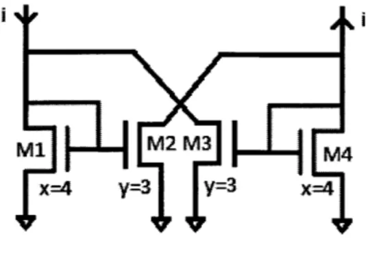
Gain
The approach taken here to derive gain in the second stage involves analyzing the current gain provided by the cross-coupled devices
M1 M2 M3 M4 (shown in Fig. 13). X and Y correspond to the
x=4 y=3 y=3 X=4 relative multiplicative factors of W in each transistor. For instance, if M2 and M3 had
Figure 13: Model of Stage 2's cross-coupled W=9=3*3, in order to fulfill the X/Y ratio in the
devices
figure, M1 and M4 would have to have W=12=4*3. Taking a step back to calculate current gain given any X and Y:
KCL applied: -i = i2 + i4 i = i1 + i3 x il = -li - -i 4 x 4 "L3 i2 ~i 3
Using the bolded equations above:
i = -i 2 ~ i4
-ii + i1
x
(x Y l1 x x ) i x-y
For the X/Y dimensions in the figure above (dimensions in original design) the current gain is 4, and therefore the overall gain of the stage is 4x the gain from the input
devices (gm/C*tint).
Noise Analysis
Noise in the second stage can be divided into that coming from the input pair, and that coming from the loads.
The noise analysis for the input pair can be found similarly to that of the one in stage
1. The only difference from the one found in stage 1 is that now the noise voltage is referred
to the input and therefore we divide E[v (ti)] by the gain squared (since we are dealing with powers).
Therefore, dividing by (Gainstage 1)2 we get:
4kTy 1
gmtint (Gainstage 1)2
Intuitively, this means that the noise voltage coming from the input pair will be significantly lower than it was in the first stage. With the DC gain in the first stage designed to be around 20, the noise voltage power of the input pair is 1/400th of that in the first stage.
Figure 14: Stage 2 Close-up of Cross-coupled loads
The noise coming from the loads can analyzed by first expressing a diode connected transistor as a 1/gm resistor (in this case mn6 and mn5), and amplifying its noise current by the current gain provided by the cross-coupled devices (mn12, mn13), 4x in this case.
4kT
vR(f) = 4kTR
--9m
IR(f) = 4kTgm
Therefore the total noise in this stage is this noise current multiplied by the current gain:
I2 = 16kTJm
Because the loads are not on at the beginning of the amplification phase, not all of the noise calculated above is actually seen by the comparator.
3.3
STAGE
3:
LATCH
AVgCr
Av Sse0
Figure 15: 65nmn Stage 3
Basic Topology and Function
The regenerative latch represents the third stage of the comparator. It includes a grounded source NMOS input pair, and cross-coupled PMOS loads. During reset, the outputs are tied to VDD, while the gates of the input pair are tied to ground (from the previous stage), allowing no current to flow through the stage at this time. During the decision phase, as the inputs of the latch increase to above VTH (of the NMOS input pair), the input pair devices turn on, discharge the output nodes, and turn on the PMOS loads, beginning regeneration.
Offset is one of the biggest limiting factors in the latch. It can be on the order of 1-5 mV, which is larger than RMS noise in most designs. In addition to this, the latch needs to be run in over-drive by a certain amount, or else it will take a very long time to achieve a certain logic level. The topology of the latch is largely limited by the 65nm process. Due to the high VTH (higher than in 0.11 m) of the devices and the low 1.2 V +/-10% supply, back to back inverters seen in many conventional latches [source] are not feasible because there is not enough headroom and the devices will go out of saturation.
Noise Analysis
Noise in a typical regenerative latch has been derived to be the following using stochastic differential equations [3]:
E [v] = c 2) e T where T =
While this equation is quite complex, intuitively there are two reasons why the latch contributes very little noise to the comparator. First, by the time the noise is referred back to the input, the gain in the first two stages is high enough that it diminishes its magnitude. Second, since the load devices of the second stage feed directly into the latch and they are shorted to ground during the reset period, the input pair of the latch isn't on during this time so its noise contribution is cut down even further.
It is important to note that offset is also an issue in comparators, and especially the latch. For applications such as this one, however, the DC offset was considered to be able to calibrated for afterwards, and was thus not a design consideration in this thesis.
CHAPTER
4:
DESIGN PORT
J2 A N ~ 2>II
s~11ktci~ -j p1~~ed 4Figure 16: 0.1.1im Comparator
In considering how to port the design of this comparator from 65nm to 0.11m, a general methodology is first introduced. When deciding how to size a transistor from the 65nm comparator to 0.11pm, the following three steps were attempted in order:
1. Keep W/L ratio the same 2. Without changing current
-1. If speed is too low
-1. Decrease load capacitances by making switches smaller
2. If speed is high enough, but not resetting properly -1. Make reset switches larger at cost of speed
3. If gain is too low or noise too high
-1. Increase gm of input pairs by increasing the size of devices 3. If performance still sub-par to 65nm
-1. Consider increasing the current, and therefore the power of the circuit
The port was done stage by stage, at each checkpoint measuring performance by comparing to that of the 65nm synonymous circuits. Each stage was optimized first for speed, then for noise and power. Speed was measured as gain observed given a certain amount of time to settle. The input of choice here is 640 gV, determined to be one of the hardest inputs for the comparator to decide on. "DC gain" means the maximum gain achieved given unlimited time allowed for settling. In the charts to follow, "W/L same" corresponds to leaving the ratio of W/L of all transistors in the stage equal to that of their 65nm counterparts, and Switches/In-pair "#W" correspond to increasing the width in the specified transistors by a factor of #. Results are grouped as follows: stage 1 alone, stage 1 and 2 together, and finally all three stages together. Therefore, each builds on the achieved performance of the last.
4.1
DESIGN PORT
+
PERFORMANCE OF STAGE
1
As seen in the chart above, Stage 1 in 65nm achieves a gain of nearly 13 in 3 0 0ps, while the ported stage 1 when
W/L is kept the same is only 6.43 (-50% slower). In order to increase the speed, the reset switch Width was quartered, bringing the gain to 9.36. The change of input pair width did not affect the gain significantly, so it was left the same. Finally, decreasing the
> Ecascode pair width by a
factor of 1/3 increased the gain to 13.26, higher than
Figure 18: Close-up of Switcses in
O,11pin Stage 1 stage 1 in 6Snm.
s= 120
vIP 1
s=,32
AVSS h
128/0.12
Figure 19: Close-up of Stage 1 input-pair in 0.11pim
First, running through a few hand-calculations it makes sense that quartering the reset switches had the effect of increasing speed, because the reset switches' Cgs and Cgd capacitances have gone down by a factor of 4, bringing the overall parasitic capacitances down by a factor of approximately 20%. Taking the slope or gm/C to be the speed of the decision with gm ~ 20mS, the speed increased roughly 30%. The actual % increase in speed from 6.43 to 9.36 is -45%, and while the hand-calculated capacitances do not give the whole picture of the speed increase, they begin to give us a clue.
Next, let us investigate why the speed did not increase when the input pair width was doubled. One of the hypotheses from the design of the stage was that if gm was increased, the speed would also increase (slope is gm/C). The first observation is that doubling the width of a device does not double its gm (as would be expected given the formula for gm in saturation is proportional to the square root of width). In fact, gm only
integrator model of speed as gm/C, the speed should have increased at least a bit. The most probable reason this didn't occur involves the size of the switches. As we saw in the process characterization chapter, as the width of a transistor increases, the output resistance decreases. Doubling the width to 1152 must have dropped the input pair's output resistance,
RDS to a level comparable to the 1/ gm that can be seen looking down into the source of the
cascode pair (see Fig. 20). At this point, some of the drain current of the input transistor
van goes back into itself as opposed to traveling down through the cascode. This means that not all of the gm Vi RDS=1/gDs is seen at the output, and the benefit of speed increase
0
is no longer seen. As a quick math check, gm of the 1/9m cascode device is roughly 19.2mS, meaning 1/ gm-52fl.In comparison, RDS for W=1152 is projected to be less
than 5kil. While this is still much higher, it is much
Figure 20: Resistances looking up and
down between the input and cascode closer to 1/ gm than at W=576, where RDS-10kU.
devices of Stage 1
Finally, the fact that decreasing cascode width by 1/3 gave a 40% speed increase should come as no surprise, because the cascode capacitance Cgd can be seen at the output. Running the same hand-calculations as above for the case of the switches, this decrease in cascode width corresponds to about a 30% decrease in capacitance on the output. Checking speed as gm/C with gm-19.2mS (assuming that the change in gm was not large, based on the small change in gm for input pair width change), the theoretical speed increase is approximately 38%, confirming the trend.
In terms of minimizing noise, the strategy was to keep the input pair gm as large as possible.
The first stage's static current is set by a current source to be 1.5mA, and therefore changes to the device sizes did not change the overall current running through them. Because the aim in this project was not to optimize power but to match the previous spec, this was a satisfactory result.
4.2
DESIGN PORT OF STAGE
2,
PERFORMANCE OF STAGES
1
+
2
Figure 21: Final Dimensions of Stage 2 in 0.11um
In 400ps, the 65nm stages 1 and 2 simulated together achieved a gain of roughly 26. At the same W/L ratio, the 0.11um stages could only reach a gain of roughly 17. Similarly to
stage 1's input pair the original strategy for the input pair was to keep it as large as possible (maximizing gm achieved was 18, in comparison to 23 seen in 65nm). However, since it is directly connected to the output of stage 1, the input pair of stage 2 now added significant parasitic capacitance of about 300fF slowing down the circuit. In order to alleviate the parasitic capacitance, the inpair width of stage 2 was cut in half, increasing speed by 17%. The switches to ground were made twice as wide as their 65nm counterparts in order to ensure proper resetting. This did not contribute to a loss in speed because these switches were smaller to begin with, and did not contribute as much to the overall capacitance on the output.
4.3
DESIGN PORT OF STAGE
3
AND PERFORMANCE OF ALL STAGES
TOGETHER
AVDD@ AVSSO sue Figure 22: Stage 3With equal W/L ratio as the 65nm comparator, the speed of the 0.11ptm comparator was 20% lower, while the noise and power were within 2% of each other. In order to match speed the current in the latch was increased by doubling the width of the input pair. This increased the overall power in the system by 11%.
4.4
RESULTS
"Speed" here is defined as the time it took for the output of each comparator to reach
0.6V, or the middle of the voltage range. It shows that the speed being the same, the noise in
the 0.11um comparator was 12.8% lower while the power was 11.1% higher. Given this trade-off between noise and power, a choice of process can be made depending on the application involved.
Another trade-off seen is the one between speed and power as well, but given the overall SAR system, speed was a limiting factor in the group's design whereas power ended up less than budgeted for (10mW spec), so the increase in power was acceptable.
The following chart describes the major noise sources of the system:
As expected, the majority of noise came from the first stage's input pair, followed by the other major components in that stage. It can also be seen that the noise contributions
by component are similar between the processes.
CHAPTER
5:
NEw ARCHITECTURE
AVDD1r
n
AVDDN m3m4 D E1AV5 152/ .12 62/0.12| " AoE o--vip. fVD virn34 AVDDD =2 Z:n =24 AV5*Figure 23: New Latch-only Architecture
Recent common comparator implementations for SAR ADCs in literature involve only one stage: the latch. This served as motivation in this thesis to implement the comparator in 0.11 m as only one latch stage. Fig. 24 shows an implementation from a 2009 paper [8],
which was followed in this thesis.
ICLK C-ICLK
OUTN OUTP There are benefits as well as drawbacks to using
ICIK a single latch stage as opposed to three stages. Because
INP*- |-eNN there are fewer components, a latch only comparator
ICLK- will be signifiCantly lower in power and faster in
Figure 24: Implementation of Latch-Only making its decisions. However, the latch also expects
to be of higher noise and offset (no preamplifier stages to reduce input-referred noise), and the input is not protected from kickback charge. Offset compensation will definitely be necessary if a latch-only architecture is used, because the amplifiers that were previously used to amplify the input signal to beyond the offset are no longer present.
One difference in the processes that allowed for the above implementation of the latch (as opposed to the 65nm latch) was the lower Vth in 0.11pm. Lower Vth allowed for the stacking of an extra pair of transistors in the latch, making it a true coupled-inverter system.
OVERALL RESULTS
. .
0.11um 510ns 61.6 uV rms 6mW
As the table above shows, the new latch only comparator achieves 40% higher speed, approximately equal input referred noise as the 65nm comparator, and 72% lower power than the 65nm comparator. As mentioned before, however, offset in the latch will be the limiting factor when deciding which topology to use.
CHAPTER
6:
CONCLUSION AND FUTURE WORK
This thesis presents the design port of a three stage SAR ADC comparator from 65nm to 0.11im, as well as a new comparator architecture in 0.11pim. The performance of the comparator in 0.11pm (especially the latch-only architecture) shows promise that the 0.11tm process is one worth going to for this specific application. The 0.11ptm design port confirmed a trade-off between noise and power, i.e. the correlation between more power (e.g. higher gm) and lower overall noise, due to the noise voltage power's inverse relationship with gm. Another trade-off was the one between power and speed - in order to achieve the same speed at the larger process node, the comparator (latch stage) needed to burn more power.
The decision to move to the 0.11 m node will most probably stem from a business perspective more than a technological limitation - whether other parts of the chip in question also benefit from being in 0.11[tm.
There are many questions left to answer in future work. What happens with different process skews? Does the system still meet specs? Why is the noise in the latch-only comparator not significantly higher than the one in 65nm? Is there a hidden trade-off that has not been looked at in this thesis? In addition, mismatches in devices were not taken into account here, so a further look into the offset of the comparator would be useful to decide whether or not it is tolerable or requires background calibration.
CHAPTER
7:
APPENDIX
Simulations were separated into three main areas: testing for speed/accuracy, testing for noise, and testing for power. Testing for power consumption involved taking time averages of the instantaneous currents flowing through the devices and due to its calculation-based nature is not featured here.
7.1 TESTING FOR SPEED/ACCURACY: HYSTERESIS ANALYSIS
The hysteresis test seen below served as the major examination tool in this thesis, which involves switching between two inputs at a certain period (2ns here for convenience) and taking a look at the output. This test provides dual benefit in that it checks whether the switches in the comparator allow it to reset properly, and also lets us compare the slope
3: 65rnm
7: 0.11um
Current: 0.11M Cross-coupled Latch alone In 64DuV/-20WV 3 (10) ? -- 4 K l: ()) -- vlop, Iom? rs. ... ..
-1
5
4 0 1.5 2 2.5 3 3.5 4 4.5 5 5.5 6 6.5 7 7.5 8 8 .5 9 9.5 10 ti- txt-9 SecoridsFigure 25: 640pV/-20ptV Hysteresis test for three comparator types
The two figures here compare the performance of the original 65nm comparator, the direct design port in 0.11 gm, and the new simplified architecture in 0.11 m. The two sets of inputs, 640tV/-20pV and 20mV/-160[tV were chosen to simulate the hardest sequence of decisions the comparator would have to make, in order to test whether it resets properly and there is no memory from the previous decision to affect the new one. For example, with an input as high as 20mV, the comparator would regenerate very quickly to 1.2V, and so the next input of -160pV would seem like a very subtle difference from 0 compared to 20mV. As can be seen in both figures, the new architecture employing only a latch clearly made a decision (increased to 1.2V or -1.2V) much more quickly than both of the other comparators.
vs 1 '5 0' -. 5 -1 -1.5 1.2 8: 0.11um 9; 65nm
Current G.11un Cross-coupled Latch Alone In > 2vIt/-160uV
s -39:(<>v13_difft() 39:(oon) ...- ,,8:(<>lo(j )~ 9:jc ol)J
It
A ~ It
1 1.5 2 2.5 3 3.5 4 4.5 5 5.5 6 6.5 7 7.5 8 8.5 9 9.5 10
ti1e, xleA Seconds
7.2 NoisE ANALYSIS: SPECTRE RF
As mentioned before, noise in the comparator is different from steady-state noise in most circuits due to its transient nature. Instead of linearizing a circuit about a single operating point, comparators require a whole period to be taken into account. For this reason, SpectreRF software was used because of its ability to provide periodic steady state (pss) and periodic noise (pnoise) analysis. Essentially SpectreRF linearized the comparator circuit around a period and used this period as a periodically time-varying operating point.
#14: 0.11um paa
#I$: 65nmpa
#53: 0.11'UM pas
Timepa Ints ta^ken, 0.6n for 014,#16, and 0.32 tor #$3 input was 60UV
12
4S:C>vfqrrt) 1.2\
0 11 17 .3 .A . .6 7 .8 .9 1 , . 2 11. 1.4 1.~ 5 18 1.17 1.8 3.9 time, K e-9 econds
Figure 27: SpectreRF pss analysis
Fig, 27 shows the pss analysis run in order to find one period within the comparator's run time. The original 65nm comparator, the direct design port in 0.11im, and the new simplified architecture in 0.11im are again compared here for one period, and it is easy to
see how much faster the simplified architecture in 0.11tm is. Fig. 29 shows the noise power of the three circuits. The noise is being integrated with frequency, so the last point of each plot is the actual noise power. The plots are misleading because in order to find input referred noise we must divide the values we see in the figure by each comparator's gain. The table on the next page shows the noise power (as read from Fig. 28), each circuit's gain, and the ratio of noise power/gain, or input-referred noise. We see that the circuit with lowest input-referred noise actually comes out to be the 0.11ptm design port, even though in the figure it is the highest curve.
415: O.ilum Noise overall, Gainr 43, Noise-616uv rms
17:h 5n Nol( overall, gain = 2.6r3, tb1'e=070,7uV rfn±
1S4: 011a FartcyLatch only Noise overall, galn2.5e3, Noise 2O.SuV rms
15:ki>nperj7o(}f) 17:(cttr.jrs(H) -- 5:<>pr00)
240
220
200
ie3 Ie4 Ie5 ie6
frecj, hertz
REFERENCES
[1] "Moore's Law" in 2009: http://en.wikipedia.org/wiki/Moore%27s law
[2] M. Yip, "A Highly Digital, Reconfigurable and Voltage Scalable SAR ADC" in Master Thesis,
MIT, June 2009
[3] AD9920a 12 bit CCD processor: http://www.analog.com/en/audiovideo-products /cameracamcorder-analog-front-ends/ad9920a/http://www.analog.com/en/audiovideo-products/product.html
[4] R. Gregorian, Introduction to CMOS OP-AMPS and Comparators, Wiley Inter-Science, United States: John Wiley & Sons, 1999, pp 182-192
[5] Sansen, W., "Challenges in Analog IC Design in Submicron CMOS Technologies." IEEE, 1996.
[6] Sansen, W., "Analog Design Challenges in Nanometer CMOS Technologies." IEEE. 2007.
[7] McCarroll, B. J., C. G. Sodini, and H.-S. Lee, "A High-Speed CMOS Comparator for Use in an ADC," IEEE J. Solid-State Circuits, SC-23, pp. 159-165, February 1988.
[8] Chen, Y., S. Tsukamoto, T. Kuroda, "A 9b 10OMS/s 1.46mW SAR ADC in 65nm CMOS." IEEE Asian Solid-State Circuits Conference, November 2009.
[9] Jeon, Y., Y. Cho et al, "A 9.15mW 0.22mm2 10b 204MS/s Pipelined SAR ADC in 65nm CMOS." IEEE Custom Integrated Circuits Conference, September 2010.
[10] Nuzzo, P., F. Bernardinis, P. Terreni, G. Van der Plas. "Noise Analysis of Regenerative Comparators for Reconfigurable ADC Architectures." IEEE Transactions on Circuits and Systems, July 2008
[11] Sepke, T., P. Holloway, C.G. Sodini, H.S. Lee, "Noise Analysis for Comparator-Based Circuits." IEEE Transactions on Circuits and Systems, March 2009
[12] Sepke, T. "Comparator design and analysis for comparator-based switched-capacitor circuits." MIT Ph.D. Dissertation, February 2007.
[13] Kapusta, R. "Comparator design review." RAK-018, July 2010.
[14] "HDMI" in July 2009, http://en.wikipedia.org/wiki/HDMI
[15] "SpectreRF,"
http://www.eecs.berkeley.edu/-boser/courses./software/spice/spectre/index.html
[16] Talekar, S.G., S. Ramasamy, et al, "A Low Power 700MSPS 4bit Time Interleaved SAR ADC in 0.18 [m CMOS," TENCON 2009.
[17] Alpman, E., H. Lakdawala, L. Richard Carley, K. Soumyanath, "A 1.1V 50mW 2.5GS/s 7b Time-Interleaved C-2C SAR ADC in 45nm LP Digital CMOS."
[18] Zhu, Y., et al. "A 10-bit 100-MS/s Reference-Free SAR ADC in 90nm CMOS." IEEE Journal of Solid State Circuits, June 2010.
[19] Jeon, Y-D., et al. "A 9.15mW 0.22mm2 10b 204MS/s Pipelined SAR ADC in 65nm CMOS."
Custom Integrated Circuits Conference, 2010.
[20] De Venuto, D., D.T. Castro, Y. Ponomarev, E. Stikvoort, "Low Power 12-bit SAR ADC for Autonomous Wireless Sensors Network Interface." IWASI 2009.
[21] Hasener, M. et al, "A 14b 40MS/s Redundant SAR ADC with 480MHz Clock in 0.13 [m CMOS." IEEE International Solid-State Circuits Conference, 2007.
![Figure 6: Dynamic Latch [7]](https://thumb-eu.123doks.com/thumbv2/123doknet/14722251.570668/11.918.569.806.90.443/figure-dynamic-latch.webp)