Design, Development and Characterization of an
Integrated Multispectral Polarimetric Sensor
System
by
Dong-Hyun C. Kim
Submitted to the Department of Electrical Engineering and Computer
Science
in partial fulfillment of the requirements for the degree of
Doctor of Philosophy in Computer Science and Electrical Engineering
at the
MASSACHUSETTS INSTITUTE OF TECHNOLOGY
May
2001
BARKER
@MMI
Massachusetts Institute of Technolog
MASSACHUSETTS INSTITUTEAll rights reserved.
OFTECHNOLOGYJUL
112001
LIBRARIES
Author...
.... .....
...
Department ofi/le trical Engineering and Computer Science
May 18, 2001
Certified by
...
...
Cardinal Warde
Professor, Department of Electrical Engineering and Computer
Science
Thesis Supervisor
Accepted by...
Arthur C. Smith
Design, Development and Characterization of an Integrated
Multispectral Polarimetric Sensor System
by
Dong-Hyun C. Kim
Submitted to the Department of Electrical Engineering and Computer Science on May 18, 2001, in partial fulfillment of the
requirements for the degree of
Doctor of Philosophy in Computer Science and Electrical Engineering
Abstract
In this thesis, a new type of integrated imaging sensor is introduced to detect multi-spectral and polarimetric signatures in an infrared scene. The sensor is a stack con-sisting of an infrared detector array, and an array of multispectral and polarimetric filters. In this first phase of the research, a single-pixel sensor was built. Multispectral filters were initially fabricated for the 3-5 micron waveband on sapphire substrates and polarimetric filters on silicon substrates. These were characterized separately and in mechanical contact as a single unit. The transmission characteristics of both filters show excellent agreement with the theoretical results. When the filters are integrated into an imaging sensor, such a sensor is anticipated to improve image contrast with sensor-fusion post processing. In addition, it will offer portability and robustness because of its integrated nature.
Thesis Supervisor: Cardinal Warde
Acknowledgments
This project was made possible thanks to the collective support of a large number of people.
The author wishes to thank Ken Vaccaro at the Air Force Research Laboratory for his helpful comments and direction, Charles Woods for his frequent discussion, and Alvin Drehman for the use of his sputtering machine. Thanks also to Professor Mark Schattenburg at Space Research Lab for his generosity with a grating simulation soft-ware packet and Professor Clif Fonstad and Professor David Staelin for their insightful input at the committee meetings.
The author is specially grateful to Professor Cardinal Warde for his continuous sup-port and valuable guidance as an advisor to this project and wishes the best luck to Dave Dunmeyer who will continue and evolve this project.
Warm cheers to many friends who have made the life at MIT bearable: Yu-chul, Tae-jung, Junbeom, Chanhyeong, Gwangpyo, Jekwan, Joonsang, Yukyoung, Yoonkyu, et.
al.
Special thanks to my family, Eunji and my parents for their eternal love and pa-tience. Thanks to my Father for his persistence and passion, who recently published 11 books and started Ph.D. study, and to my Mother for pushing me with her inde-fatigable desire to learn.
This research was sponsored by the Air Force Research Laboratory under contracts F19628-99-C-0052 and F19628-00-C-0002. Support from MIT Lincoln Laboratory is also gratefully acknowledged.
Contents
1 Introduction 15
1.1 Overview of Thesis . . . . 17
2 Background 19 2.1 Polarization in Nature . . . . 19
2.2 Emission Polarization vs. Reflection Polarization . . . . 20
2.3 Stokes Parameters and Mueller Matrix . . . . 21
3 Related Work 25 3.1 Multiple-polarization/multiple-band systems . . . . 25
3.1.1 Earth Observing Scanning Polarimeter (EOSP) . . . . 25
3.1.2 Polarization and Directionality of Earth Reflectances (POLDER) 26 3.1.3 Acousto-Optic Imaging Spectropolarimeter (POLARIS II) . . 27
3.1.4 Fourier-Transform IR Spectropolarimeter (FTIRSP) . . . . 28
3.1.5 Remote Minefield Detection System (REMIDS) . . . . 28
3.1.6 Imaging Multispectral Polarimeter . . . . 31
3.1.7 Prism spectrophotopolarimeter . . . . 31
3.2 Multiple-polarization/single-band systems . . . . 31
3.2.1 MWIR Polarization Sensitive Thermal Imager . . . . 31
3.2.2 Diffraction-Grating Photopolarimeter . . . . 32
3.2.3 Airborne MWIR Polarimetric Imager . . . . 33
3.2.4 Prism-based Imaging Polarimeter . . . . 34
3.2.6 Wire-grid Polarizer Arrays Patterned with Microlithography . 4 Integrated Multispectral Polarimetric Sensor
4.1 Approach ... ...
4.2 Multispectral Filter Design and Fabrication 4.2.1 M aterials . . . . 4.2.2 Computation of the Filter Structure . . 4.2.3 Filter Fabrication . . . .
5 Polarization Filter Design and Fabrication 5.1 Model Used in the Simulation
5.2 Theoretical Background . . . 5.3 Simulation Results . . . . 5.3.1 Grating material . . . 5.3.2 Substrate . . . . 5.3.3 Grating pitches . . . . 5.3.4 Grating height . . . . 5.3.5 Duty cycle . . . . 5.3.6 Higher-order diffraction 5.3.7 Over-etch . . . . 5.3.8 Under-etch . . . . 5.3.9 Finite aperture . . . . 5.4 Filter Fabrication . . . .
6 Multispectral and Polarization Filter 6.1 Multispectral Filter . . . .
6.1.1 FTIR measurements . . . . . 6.1.2 Measurement with a Pt-Si can 6.2 Polarization Filter . . . . 6.2.1 6.2.2 Characterization
. . . .
era . . . .. . . .
Brief discussion about optical set-up: reflective or transmissive Unpolarized FTIR measurement of Al/Nb/Ti on a Si substrate
36 39 39 41 41 42 48 51 51 52 53 53 56 56 56 59 59 62 62 62 65 67 67 67 69 75 78 78
6.2.3 FTIR measurements using a ZnSe wire-grid polarizer . . . . . 78
6.2.4 Instrument effects in the polarization characterization . . . . . 81
6.2.5 Characterization with the Pt-Si camera . . . . 81
6.3 Multispectral and Polarization Filters in Mechanical Contact . . . . . 83
6.3.1 M easured results . . . . 83
6.3.2 Characterization with the Pt-Si camera . . . . 87
7 Future Directions and Concluding Remarks
91
7.1 Future D irection . . . . 917.1.1 Flat Transmittance Characteristic of the Polarization Filter . 91 7.1.2 Two Polarizers in Series . . . . 93
7.1.3 Hyperspectral Filter Using Non-Uniformity . . . . 93
7.1.4 Integrated Multispectral Polarization Filter . . . . 93
7.2 Concluding Remarks . . . . 97
A Program Code to Design a Multi-layer Interference Filter Based on
Simulated Annealing
99
A.1 FilterOptimization.c - non-dispersive materials . . . . 99A.2 FilterOptimization.c - dispersive materials . . . . 103
A .3 M yM ath.c . . . . 108
A.4 FilterOptimization.h . . . . 109
B Material Data in Gsolver.ini
111
List of Figures
1-1 Integrated multispectral polarimetric sensor in an infrared camera and
its desired features . . . . 17
3-1 Instrument operation of the POLDER . . . . 26
3-2 Basic operation of the Acousto-Optic Imaging Spectropolarimeter, PO-LA R IS II . . . . 27
3-3 Schematic diagram of the Fourier-transform IR spectropolarimeter sys-tem . . . . 29
3-4 The active/passive system operation of the REMIDS . . . . 30
3-5 System diagram of the polarization sensitive thermal imager . . . . . 32
3-6 Diffraction grating photopolarimeter . . . . 33
3-7 Schematic diagram of the Airborne MWIR Polarimetric Imager . . . 34
3-8 Prisms for imaging polarimetry (a) Wollaston (b) Rochon . . . . 35
3-9 Structure of the wedged double Wollaston prism . . . . 37
3-10 ematic diagram of unit cell containing a 2x2 array of micropolarizers . 38 4-1 Schematic diagrams of the multispectral polarimetric sensor . . . . . 40
4-2 Flow chart for optimization of multispectral filters based on simulated annealing . . . . 43
4-3 Optimum structure of the multilayer subfilters on GaAs . . . . 45
4-4 Optimum structure of the multispectral filters calculated for sapphire substrates ... ... 46 4-5 Sensitivity of the multispectral filter to thickness variation in the layers 47
5-1 Schematics of the model in the wire-grid polarizer simulation . . . . . 52
5-2 Qualitative description of why Rayleigh anomaly is outstanding for TM polarization . . . . 54
5-3 (a) Above, TM transmittance of the polarizer for each material (b) Below, extinction ratio of the polarizer for each material . . . . 55
5-4 Effects of pitch for TM transmittance of the polarizer . . . . 57
5-5 Effects of grating height on TE and TM components . . . . 58
5-6 Effects of grating duty cycle for TM transmittance of the polarizer . . 60
5-7 Higher-order components of a polarizer . . . . 61
5-8 Effects of over-etch . . . . 63
5-9 Effects of under-etch . . . . 64
5-10 Processing flowchart for wire-grid polarization filter . . . . 65
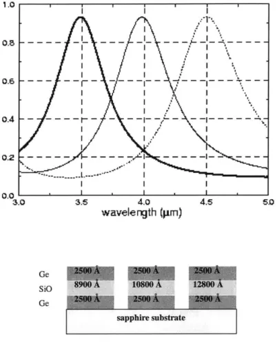
6-1 Measured transmittance of Ge/SiO/Ge/SiO on a GaAs substrate . 68 6-2 Measured transmittance of Ge/SiO/Ge on a sapphire substrate. . . 70
6-3 Adjusted spectral characteristic of the measured Ge/SiO/Ge sample on a sapphire substrate . . . . 71
6-4 Optical set-up used to characterize a multispectral filter . . . . 72
6-5 Emission images of a blackbody object at different temperatures . . . 73
6-6 Reflection images of a blackbody object at different infrared source temperatures (I is the current to the light source.) . . . . 74
6-7 Imaging experiment of the multispectral filter based on blackbody ra-diation . . . . 76
6-8 Polarization characteristics of the Nicolet 860 FTIR System . . . . . 77
6-9 Calculation vs. unpolarized FTIR measurement results . . . . 79
6-10 Measurement results of the three sub-stripe polarization filters using F T IR . . . . 80
6-11 Instrument effects in the polarization characterization . . . . 82
6-13 Transmission images of the polarization filter at different polarizer
ori-entation . . . . 84 6-14 Measured results using FTIR for all combinations of multispectral
pass-bands and polarization filter orientations . . . . 85 6-15 Intensity as a function of wavelength for the subpixel corresponding to
horizontal polarization and 3.5 - 4.5pm waveband with source polar-ization angle 0 . . . . 86 6-16 Optical set-up for multispectral polarization filter samples . . . . 87 6-17 Transmission images of multispectral and polarization filters at
differ-ent source temperatures ... ... . . . .. . . . . . 88 6-18 Transmission images of the multispectral and polarization filters in
mechanical contact at different polarizer orientation . . . . 89
7-1 Transmittance of the metal wire-grid grating of multiple linewidths . 92 7-2 Processing flowchart for the triple-decker spectral polarizer plate on a
com m on substrate . . . . 94
7-3 Processing flowchart to integrate the triple-decker spectral polarizer to a sensor on a single substrate . . . . 95
Chapter 1
Introduction
A sensor is a device used to sense or measure physical phenomena. Sensors detect electrical, mechanical, optical, chemical, tactile, and acoustic signatures, for exam-ple, from background, and they extract and provide the basic information about objects. Objects that may be difficult to discriminate using a single sensor are often differentiated with a multiple sensor system that exploits several signature generation phenomena to gather data about the scene of interest. The application of multiple sensors (and the fusion of their data) offers numerous potential performance benefits over traditional single sensor approaches. Employing multiple sensors, which respond to different signatures, increases the probability that an object signature will be found against a given set such as weather, clutter, or background. Multiple sensor systems, in other words, diminish ambiguity and uncertainty in the measured information by reducing the set of hypotheses about the object or event. Multiple sensors may also be used to reduce the vulnerability to false conclusions drawn from single-sensor data. For instance, missiles may carry multiple sensors to better guarantee a hit or a radar can use multiple sensors to counter-jam incoming missiles.
The goal of the research carried out in this thesis is to develop and explore the feasibility of an integrated sensor (with no moving parts) that can record the multi-spectral and polarization signatures of infrared scenes, so that one can subsequently achieve improved image contrast from the measured information.
the object could depend on the surface coating of the object and/or chemical com-position of man-made materials. Moreover, multispectral data are significantly less sensitive to viewing geometry and surface smoothness than are polarization data. On the other hand, polarimetric measurement takes advantage of the fact that natural backgrounds show generally little or weak polarization signatures, while man-made objects tend to radiate with polarization component[1]. A recent study for the 3-5pm waveband demonstrates that the polarized signatures of many natural objects were measured less than 0.2%, compared to 2-4% degree-of-polarization for man-made ground objects[2, 3]. In addition, polarization data often contain information about the surface orientation and/or surface properties of objects, and a polarization signal can exist even when no intensity contrast is present[4, 5]. Consequently, it is believed that polarization and multispectral imaging data are complementary. By combining the two, better contrast can thus be achieved, since they depend on different optical characteristics of the object. However, it is not clear yet what combinations of po-larization and spectral measurements are optimal for object discrimination in a given scenario, for so little data have been taken in natural and man-made scenes.
This study explores the integrated nature of multiple sensor fusion by designing and building a smart-pixel sensor. This sensor integrates optical components that can determine spectral content, polarization state and intensity level in each pixel. One can use the integrated sensor in an infrared camera as shown in Figure 1-1 and then post-process the multiple outputs of each pixel with a neural-network based sen-sor fusion processen-sor to perform object discrimination. This approach is anticipated to permit highly selective discrimination among objects with nearly identical spatial and spectral features, along with the compactness, portability, ruggedness and sig-nal processing strengths achieved through the use of semiconductor integrated circuit technology. Note some desired features of the integrated sensor in Figure 1-1.
Integrated multispectral polarimetric sensor array
Infrared Camera
Figure 1-1: Integrated multispectral polarimetric sensor its desired features
Key Features
(1) no moving parts (2) high sensitivity (3) high contrast (4) compact (5) readily packaged into camera (6) software interfacein an infrared camera and
1.1
Overview of Thesis
The next chapter describes background information to understand the environment where the proposed sensor system is to be used. This is followed by the chapter that recapitulates various multispectral polarimetric filtering strategies that have been attempted in the past. Subsequent chapters begin with a presentation of a new approach to tackle this problem, and discuss issues related to the design, fabrication, and characterization of the proposed multispectral polarimetric sensor device. Finally, the improvements and future directions are described with concluding remarks.
Appendices include the custom-made source code to design an optimum multispec-tral interference filter. Also included are some material parameters for the simulation of wire-grid polarization filters. Vendor information who supplied essential parts for this project is shown in Appendix C.
Chapter 2
Background
This chapter describes some basic facts about the polarization of light scattered from natural objects such as vegetation, terrain, lakes and rivers, and briefly discuss emis-sion and reflection polarizations. In addition, this chapter also discusses man-made objects made of natural materials and the polarization characteristics of such objects.
2.1
Polarization in Nature
As was stated in Chapter 1, polarized light exists in nature. Two most well-known examples are light scattered by the air molecules in the blue sky and light reflected off water. The overhead blue sky is strongly polarized at 900, from the sun, with its degree of polarization reaching a maximum value of about 75% at twilight. When the sky is clouded, the light is linearly polarized with its orientation determined by the illumination[6]. Cloud particles directly lit by the sun or the moon, acting as a reflecting surface, polarizes light tangentially, as in the case of the blue sky. The degree of polarization, however, may differ depending on the particle characteristics, such as composition, density and size. On the other hand, still water acts as a large reflecting surface. The reflected light is 100% linearly polarized at the Brewster angle of about 370, to the surface.
Much part of the polarization that is observed in nature is linear polarization, oftentimes, with a reduced degree of polarization. The polarization phenomena in
nature need to be analyzed to be isolated, when the polarization sensor is to be used against the sky or the water, such as ocean or lakes.
Not all polarizing objects are linear polarizers. Some materials such as birefringent polymers and, most notably, nucleic acids convert unpolarized light into circularly polarized light upon reflection. This is due to the helical structure of the molecules the metals are composed of. Therefore, when linearly polarized light is incident, only one form of circularly polarized light is reflected. This phenomenon is called circular
dichroism[7], which may potentially pose a problem for an incomplete sensor that discriminates only linear polarization. However, the polarization that can be found in nature is dominantly linear polarization. For example, it was reported that in the case of water surface, the contribution of the circular polarization component to the total intensity is two orders of magnitude less than that of the linear polarization component[8]. Thus, the needs to detect circular or elliptical polarization may be marginal.
2.2
Emission Polarization vs. Reflection
Polariza-tion
Polarization characteristics of an emissive object is very different from that of a reflec-tive object. Light, reflected by a smooth surface, is polarized tangentially. Its degree of polarization becomes maximal, when the light is reflected at Brewster angle. On the other hand, the emitted light, after refracted by and transmitted through a sur-face, is polarized vertically, assuming that the direction of the emission is statistically random with its irradiance governed by the cos4O law and that there is no oxide layer which destroys polarization[9]. In addition, the emitted radiation is never polarized as much as may be possible in reflection. For this reason, it would be very tricky to exactly tell the polarization characteristics of an object in a hot daylight environment, unless the data of the object are well analyzed a priori at a given temperature and geometry.
2.3
Stokes Parameters and Mueller Matrix
Stokes parameters are a four-parameter representation of the state of polarization of light. For a quasi-monochromatic plane wave, they are the four quantities defined as
2 2
S,= < a2 > < a >
S1 =
S2= 2 < ala2cos6 >,
S3 = 2 < aja2sMn >, (2.1)
where a, and a2 are the instantaneous amplitudes of the two orthogonal components
E, and E, of the electric vector and 6 is their phase difference. In order to see how
Stokes parameters can be useful to characterize the polarization state of light, consider a quasi-monochromatic light with a frequency
f
propagating in the z-direction. This can be expressed asE,(t) =a(t)eq[jt)27ft]
Ey(t) = a2(t)e[02(t>27ft]. (2.2)
Since the electric vector that makes an angle 0 relative to the positive x axis is
E(t) = Ecos0 + Eye asin, (2.3)
where a is the retardation of the y-component with respect to the x-component. Therefore, the observed intensity of the light, when transmitted through a polarizer with the appropriate orientation, is
I =< E(t)E*(t) >
= < EE* > cos20 + < > sin20
Using Equation 2.2 and Equation 2.4,
I <a> cos2
<
a> sin20+ < a1a2ei(1-2) > e-iacossin0 + < aia 2ei(O1 02) > eacos~sinO. (2.5)
Since the retardation is ignored for incomplete sensor systems which measure linear polarization only,
I = <a2 > cos20 + <a2 > sin 20+ < aia2cos( 1 - 02) > sin(20)
= <a1 > cos2 +
< a2
> sin20+ < aia2cos6 > sin(20), (2.6)where 6 = 0 -
#
2. From Equation 2.1 and Equation 2.6, So = I( = 00) + I(0= 900), S1 = I( = 00) - I(= 900),S2 =
1(0
= 450) -1(0
= 1350). (2.7)S3 cannot be directly obtained for incomplete systems. For a quasi-monochromatic plane wave, however,
SS ~S +S+ , (2.8)
which can be used to indirectly obtain S3. In general, S3 represents the amount of circularly polarized light and is usually very small. For incomplete systems, this parameter may be ignored. Note that from Equation 2.6,
1(0
= 1350) =1(0
= 450) -[1(0
= 00) +1(0
= 900)]. (2.9)This means that only three independent intensity measurements of a polarizer with an orientation at 00, 450 and 900 are necessary to characterize the state of polarization of the incident light. In terms of the Stokes parameters, the degree of polarization of light is defined as the ratio of intensity of polarized light component to total light
intensity. In other words, the degree of polarization
P = Ipolarized/Itotal
= S2 + S2 + S3/2SO, (2.10)
expressed in %. The degree of polarization is a good measure of the light polariza-tion. For example, 0 or 100% of the degree of polarization indicates that the light is unpolarized or perfectly polarized, respectively.
While Stokes parameters are used to understand the polarization characteristics of incident light, the Mueller matrix is a 4x4 matrix representation of an optical component, which completely describes how the component affects the polarization of the partially polarized incident light. The Stokes parameters after light is sent through an optical component can be calculated by multiplying the input Stokes vector, a column vector the Stokes parameters are grouped into, with the Mueller matrix of the component. Some of the most useful Mueller matrices are collected in
[10].
Chapter 3
Related Work
There have been continuing efforts to build multispectral and/or polarimetric sensors for a variety of applications in astronomy and Earth sciences. Recently, such sensor systems have been seriously developed for remote sensing and military applications. Some of the previous approaches to multispectral and/or polarimetric sensors are reviewed in what follows.
3.1
Multiple-polarization/multiple- band systems
3.1.1
Earth Observing Scanning Polarimeter (EOSP)
The EOSP[11, 12, 13, 14] is an instrument, developed for Earth Observing System (EOS) space mission platforms at NASA in late 1980s and early 1990s, to provide global mapping with multispectral photopolarimetry. Even though the EOSP was not launched as of 2000, this would allow more pronounced aerosol signature in the polarization of the scattered light, compared to the radiance. The EOSP scans a con-tinuous sweep of the instantaneous field of view (IFOV) of the scene. The scanned scene is supplied to eight boresighted telescope and aft optics assemblies simultane-ously, each of which angularly separates the incident scene flux into two orthogonally-polarized beams. Each beam is then spectrally separated into three spectral bands using dichroic beamsplitters and bandpass filters. The spectral band of the system
CCD Sensor
Multispectral filter Polarization filter
Spinning filter wheel
Wide FOV optics
Figure 3-1: Instrument operation of the POLDER
thus covers 12 discrete passbands, ranging from 410nm to 2250nm.
3.1.2
Polarization and Directionality of Earth Reflectances
(POLDER)
The POLDER[15] is an optical imaging radiometer, developed at CNES (Centre Na-tional d'Etudes Spatiales) of France and installed on the satellite of the Japanese
ADEOS mission in 1995. It scans a wide field of view (500) with moderate spatial
resolution (6 x 6 kM2) and observes bidirectional reflectance and polarization
distribu-tion of the scanned scene on a global scale by taking, for a given object, measurements in variable viewing configurations along the track of the satellite. The radiation from the scene is time-multiplexed by the fast-spinning spectral filters in nine spectral bands of the visible - near infrared spectrum. Polarization states are measured at three of the nine wavelengths. The instrument is schematically described in Figure
Elliptical mirrors
Flat reflectors
o-beam
o-image
Input beam -- difracted CCD Camera
e-image Acousto-optic
tunable filter e-beam
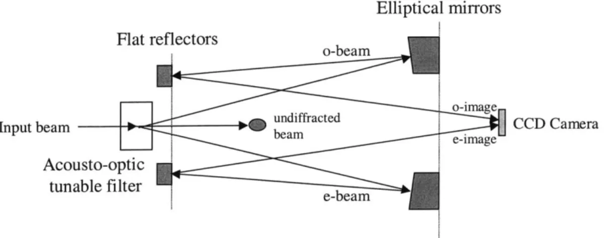
Figure 3-2: Basic operation of the Acousto-Optic Imaging Spectropolarimeter, PO-LARIS II
3.1.3
Acousto-Optic Imaging Spectropolarimeter (POLARIS
II)
POLARIS II[16] is an imaging spectropolarimeter for ground-based astronomy, based on acousto-optic tunable filter(AOTF), constructed at NASA/GSFC(Goddard Space Flight Center) in 1989. The key component of the system is the AOTF crystal which diffracts an incoming light into different directions according to the wavelength and the polarization state of the light, when the acoustic wave propagates through the crystal. When the incoming beam leaves the AOTF, the beam becomes diffracted with
+1 and -1 orders, polarized orthogonally to each other. These o-beam and e-beam are imaged onto different parts of a CCD camera. The basic operation of POLARIS II is shown in Figure 3-2. The system is limited by the material properties of an AOTF. Also, the wavelength tuning range is fundamentally restricted up to near infrared and only two linear polarization components are allowed by the AOTF crystal.
3.1.4
Fourier-Transform IR Spectropolarimeter (FTIRSP)
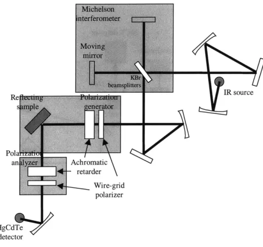
The FTIRSP measures the infrared Mueller matrix spectrum in transmission or re-flection at 450 from a sample under test[17, 18]. The schematic diagram of the system is shown in Figure 3-3, where Michelson interferometer provides a sample beam of se-lected wavelength out of global IR source by fine-tuning the position of a mirror. The whole spectrum thus covers 2.5 - 14pm. The polarization generator, composed of an achromatic retarder and a wire-grid polarizer, then polarizes the incident monochro-matic light along the desired polarization direction. After the beam is scattered by the sample, its polarization state is analyzed by the polarization analyzer. The Mueller matrix of the sample for specific wavelength and incident angle(45") can be deter-mined from the data. Applications include testing of polarization elements such as electro-optic modulators, IR polarizers, and retarders and IR signature modeling of military target samples. A similar system to this measures 16 elements of a sample's Mueller matrix[19].
3.1.5
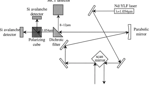
Remote Minefield Detection System (REMIDS)
The REMIDS[20] is a multi-channel active/passive sensor system, developed by U.S. Army since early 80s and operated on U.S. Army UH-60A Black Hawk helicopter to characterize sizes that have landmines present. Figure 3-4 shows the basic opera-tion of the REMIDS. The system has 6 separate channels which include active laser reflectance measurements of p- and s- polarization components using Nd:YLF laser at A = 1.053pm and passive thermal emission measurements for A = 8 - 12pm. In the collected radiation focused by a parabolic mirror, the thermal energy is separated from captured portion of the scattered laser light by a dichroic beamsplitter. The laser light is then split into two polarization components by a beamsplitting cube. The experimental demonstration in 1990 and 1991 showed successful results, even though the results were found to be site-dependent. For example, the detection percentage exceeded 95% for surface-type landmines.
Re .httr IR source s mple eneratobr. Pola an yzer Achromatic I -retarder Wire-grid polarizer HgCd4Te detector
MCT detector
Si avalanche
detector
Nd:YLF laser -=1.054 mSi avalanch
i
detector
8~12ptm 1.054UnNPolarizing
Dichroic
cube
filter
scan mirrorFigure 3-4: The active/passive system operation of the REMIDS
Parabolic
nirror
3.1.6
Imaging Multispectral Polarimeter
In this system[21], which was developed in 1998 by the Applied Technology Associates sponsored by the Air Force Research Lab, multispectral filtering is performed with a fast spinning spectral filter wheel that contains eight spectral filters. The spectral filter was created to run fast enough to produce Stokes images in a minimal time before the scene changes significantly. A complete Stokes vector of a given scene can be measured with a combination of a rotating quarter wave plate and a stationary linear polarizer in addition to the spinning spectral filter wheel. Operating range of wavelength is 0.6 - 0.85pim.
3.1.7
Prism spectrophotopolarimeter
This system is an instrument to take radiometric and polarimetric measurements for astronomy, developed in 1992 by National Observatory of Japan[22]. The system is not a true spectropolarimeter in the sense that the radiometric and polarimetric measurements are not taken at the same time and the conversion between photometric and polarimetric modes is done by inserting or retracting a half-wave plate and a CaF2 wire-grid polarizer, which takes about 5 minutes. The spectrometer employs a sapphire prism that disperses incident infrared light and refocuses it onto the 16-channel detector array. The system covers 0.9 - 2.5btm with a resolution of 0.1pm.
3.2
Multiple-polarization/single-band systems
3.2.1
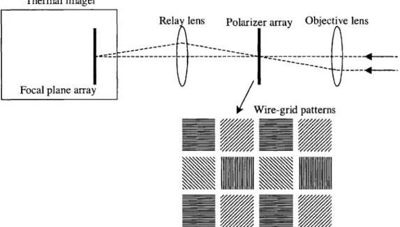
MWIR Polarization Sensitive Thermal Imager
The main objective of this system[23] is to take advantage of the polarization sen-sitivity to surface orientations for automatic object recognition. In the system, as shown in Figure 3-5, the radiation from objects, after transmitted through wire-grid polarizer array, is imaged on the thermal imaging focal plane array. The wire-grid polarizer has three angular orientations, patterned using microlithography. The wave-length range that the system covers is 3 - 5pim. Few results, however, were obtained
Thermal imager
Rela lens Polarizer array Objective lens
---- --- - - -- - - - - - -- - - - -
-Focal plane array
/
Wire-grid patterns
Figure 3-5: System diagram of the polarization sensitive thermal imager
experimentally.
3.2.2
Diffraction-Grating Photopolarimeter
Diffraction grating is used to make a division-of-amplitude photopolarimeter[24, 25]. This is shown in Figure 3-6. The incident light beam is diffracted by a diffraction grating and the diffracted orders are polarized by the linear polarizers in front of photodetectors at different orientations. From the detected photocurrents, four Stokes parameters are then extracted from the measured data. The dispersive nature of the system poses a significant limit on the system performance. Namely, if this system is to be applied for spectrophotometry, the system would require very high-resolution detector arrays. This is even worse for imaging spectrophotometry, which makes this
-1st-order
I
st-order2nd-order
Input light
Figure 3-6: Diffraction grating photopolarimeter
system too complicated for practical purposes.
3.2.3
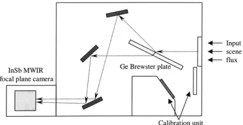
Airborne MWIR Polarimetric Imager
This MWIR imager was developed at the Environmental Research Institute of
Michi-gan (ERIM) around 1996. Figure 3-7 shows the schematic diagram of this system.
The incoming scene flux is divided into two polarization components by Ge Brewster
plate[26]. Each of the polarized scenes from both reflected and transmitted beams is
imaged sequentially in time on the IR camera. The most critical issue of the system is
the band-to-band channel misregistration, which arises due to the sequential nature
of the system. If channels are not precisely registered, unpolarized spatial variations
in the background can leak through and appear as polarized radiance. The system
InSb MWIR focal plane camera
Ge Breste p e
..
-Ge Brewste plate
--Calibration unit
Figure 3-7: Schematic diagram of the Airborne MWIR Polarimetric Imager
operates for 4.6 - 4.9pim band at a 52Hz frame rate and has been used to collect background data ranging from rooftop, tower, fixed wing, military targets and also natural backgrounds such as vegetation and cloud.
3.2.4
Prism-based Imaging Polarimeter
This system[27] is based on a Wollaston prism or a Rochon prism to split light accord-ing to the polarization. Both Wollaston and Rochon prisms are basically a combina-tion of two triangular prisms with optical axes at different orientacombina-tions. As shown in figure 3-8, Wollaston prism allows bigger separation angle between two polarization components than Rochon prism, which makes Wollaston prism structure more advan-tageous for a polarimeter. While the system is relatively easy to set up using just one composite prism, it is not complete in the sense that it can tell only two polarization components. The wavelength coverage is limited by the prism, which usually covers up to near infrared.
4- Input 4 scene 4- flux
Og 0.00 S .0 0000 00000 0. gee 0. * @0 * Og * 0. * 0.. * * 0.
Top view
TE
0--TM
(a)
Top view
,TB
(b)
Figure 3-8: Prisms for imaging polarimetry (a) Wollaston (b) Rochon
-0-. *
3.2.5
Single Shot Polarimetry Using Wedged Double
Wollas-ton
This system was first proposed in 1996 for astronomical spectropolarimetry[28]. The system is based on a combination of two Wollaston prisms and two wedges, as shown in Figure 3-9. This wedged double Wollaston prism is inserted in the pupil plane of a camera and spectrometer and the polarized flux at 00, 450, 90', and 1350 is
simultaneously measured. The two wedges split the image and deviate all rays above and below the optical axis. The four images, after two Wollaston prisms above and below, correspond to measurements performed with polarizers at 01, 450, 90' and 135'.
From the data, the first three elements of the Stokes vector are determined without rotating half wave plates. The prism combination was optimized for 0.3 - 2.5pm.
3.2.6
Wire-grid Polarizer Arrays Patterned with
Microlithog-raphy
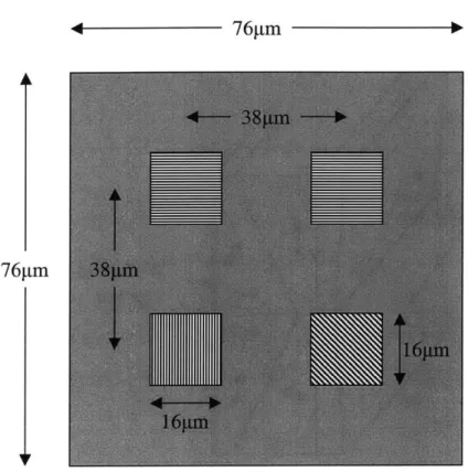
Arrays of 256 x 256 micropolarizers at three angular orientations were fabricated that measure the first three Stokes vector components in each pixel of an imaging polarimeter for the 3 - 5pm range[29]. Each micropolarizer consists of a 475 nm-period Mo wires in a 16pm x 16pim aperture. The schematic diagram of unit cell is shown in Figure 3-10. Interference lithography is used to generate the small grating features through an etch mask layer. Even though an imaging system composed of a micropolarizer array integrated directly onto a focal plane array was assembled, and initial testing was performed, this research is still in the development phase and practically meaningful data still remain to be taken.
It is interesting to note that the majority of the previous systems do not operate in MWIR (3 - 5tm) range due mostly to the wide availability of the off-the-shelf discrete optical elements for visible and near infrared bands. None attempted to integrate polarizers with spectral filters in a compact single package with no moving parts. This may be due to the difficulty associated with the fabrication of the polarizer, in contrast to the relative facility to form a system with discrete elements.
0=90'
0=135'
0=45*
Wollaston
prism
Figure 3-9: Structure of the wedged double Wollaston prism
wedge
76pm
76gm
Figure 3-10: ematic diagram of unit cell containing a 2x2 array of micropolarizers
1
p-Chapter 4
Integrated Multispectral
Polarimetric Sensor
4.1
Approach
The general approach of the research described in this thesis is to design and build a smart-pixel sensor which integrates optical components that can determine spectral content, polarization state and intensity level in each pixel, and which can then post-process the multiple outputs of each pixel with a neural-network based sensor fusion processor to perform object discrimination.
Figure 4-1 shows the schematic diagram of the two different structures for the sensor. The triple-decker system on the right has a multi-layer interference filter and wire-grid polarizer on top of each other, while they are laid side-by-side in the double-decker system on the left. Compared to the double-decker, the triple-decker has lower resolution and is less power-efficient. The triple-decker system, however, has the data from spectral and polarization sub-pixels perfectly registered, and moreover, it is relatively simple to fabricate due to its planar structure, lending itself to the only practical alternative for the study.
The multispectral polarimetric sensor system based on this scheme is not com-plete, in the sense that the system cannot distinguish circular polarized contents from unpolarized light. While it is not easy to integrate any features for circular
polar-Polarization filter Multispectral filter Detector
Substrate
(a) Double-decker design
Polarization filter 1+ Multispectral filter
Detector Substrate
(b) Triple-decker design
ization, the incompleteness may not be such an issue, since most of the natural and man-made objects polarize linearly with a few exceptions, as was briefly discussed in Chapter 2. Another potential issue with the proposed scheme in Figure 4-1 is that the spatial resolution of the system is inversely proportional to the spectral and po-larimetric resolution. For this reason, it is important to estimate an optimal number for the spectral and polarimetric resolution. The system described in this thesis work has three spectral bands, equivalent to the three primary colors, and three polariza-tion orientapolariza-tions, which is the minimum number required to tell linear polarizapolariza-tion contents in an incident scene.
In the first phase of the overall program (the scope of this research), a discrete-component approach with a large pixel size was first taken to establish the operational feasibility of such a sensor concept in the 3 - 5pm waveband. Individual components, and a spectral polarizer plate formed by sandwiching multispectral and polarization filters in mechanical contact were evaluated using a commercially available Pt-Si camera.
In the next step, the details of which are beyond the scope of this thesis, integration of multispectral and polarization filters on a common substrate will be attempted. This will be eventually followed by integration with a detector and then using sensor fusion algorithms such as the opponent processing models[30] to analyze the sensor data for object discrimination purposes.
4.2
Multispectral Filter Design and Fabrication
4.2.1
Materials
Germanium (Ge) and silicon monoxide (SiO) were used as high and low index ma-terials of the multispectral filter, respectively. They are transparent over the wave-length range of interest and their refractive index difference is very large (An = 2.24 at A = 4.0p/m). In addition, they show good deposition characteristics on sub-strates such as sapphire, Si and GaAs, and are robust to the atmosphere. Ge is
widely available and is used as the high index material (refractive index n = 4.04 at A = 3.Opm)[31, 32, 331; it is transparent in the 2 - 15pm wavelength range. On the other hand, SiO is often used as a low-index material up to a wavelength of 7pm for infrared multi-layer filters. Its index of refraction is 1.80 at 4.Opm[34]. From a processing perspective, SiO is compatible with other oxides and metals such as Si, Ge, and Al. SiO is also used as a protective over-coating for aluminum mirrors and as an anti-reflecting layer in optical applications.
The substrates on which the sensors were built are sapphire and GaAs. Sapphire is very hard and robust, and transparent in the wavelength range 0.14 - 6.5pm. GaAs has advantages over sapphire in terms of photolithographic etching and processing, and availability.
4.2.2
Computation of the Filter Structure
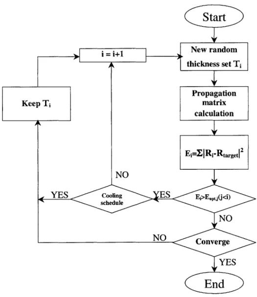
Since general design methods[35, 36], using equivalent layers or based on Chebyshev polynomials end up with a large number of layers, three multispectral sub-filters were designed using a propagation matrix approach[37, 38], and a simulated anneal-ing algorithm[39]. Target wavelength transmission peaks were at 3.5p-Lm, 4.0pim and 4.5[pm and the half width of each band was chosen to be 0.5pum so that there was some overlap between adjacent bands. The propagation matrix corresponding to each interface between different materials is multiplied, after random numbers are assigned to each layer as thickness values. This set of thickness values is taken for the next loop, when the reflectivity calculated from the propagation matrix is closer to the desired reflectivity than in previous loop, or depending on a statistic instituted by the cooling schedule of the simulated annealing algorithm.
Figure 4-2 describes the procedure of this design process. Priority was given to the structure with the least number of layers in each sub-filter and that simultaneously had the largest number of common layers for the three sub-filters. This was done in order to simplify the fabrication process. The importance of minimal number of layers is very clear in a work[40] that attempted to implement a multispectral interference filter with 33 layers of Ge and SiO films and was plagued by a number of problems
Start
. .+ New random thickness set TjPropagation
Keep Tj
matrix
calculation
Ei=XjRi-Rtarget| 2NO
YES
Cooning
ES
E>E,jschedule
NO
NO Converge
YES
End
Figure 4-2: Flow chart for optimization of multispectral filters based on simulated
in building a filter more than 6mm thick. Since the interference filters are optimized only for the 3 - 5pm range, it is necessary to cascade the interference sub-filters with long-pass and short-pass absorption filters to reject light outside this region. For a sapphire substrate, the substrate itself can serve as the short-pass filter since its cutoff wavelength is about 6.5pm.
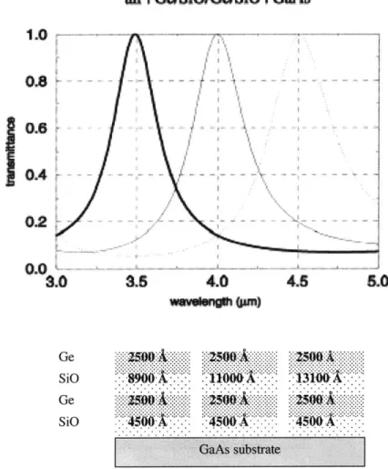
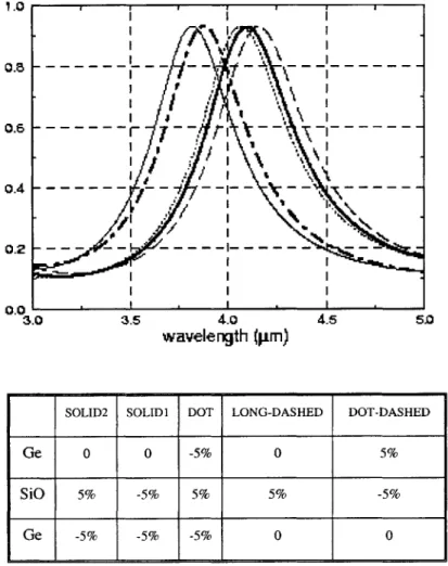
Figures 4-3 and 4-4 show the simulated transmittance curves for the optimum structures on GaAs and sapphire substrates, respectively. Notice that for sapphire substrates, the three-layer structure (without the first SiO layer) performs just as well as the four-layer structure. For Si or GaAs substrates, three layers never gave satis-factory results. Note that the only structured difference between the three sub-filters is the thickness of the middle SiO layer, which shifts the passband. Also note that the thickness of both Ge layers in each sub-filter is the same (2500
A).
This approach, indeed, minimizes the number of sputtering and etching step necessary to make the filters. For example, for a four-layer structure on a Si or GaAs substrate, only two sputtering runs, rather than 12, are needed to make a three sub-band multispectral filter.The sensitivity of the sub-filter transmission characteristic to potential fabrication errors in the process of thin-film deposition is described in Figure 4-5. This figure was generated for the waveband that peaks at 4pLm, assuming 5% of error in some of the film thickness. A three-layer structure was assumed on a sapphire substrate for this figure. It is clear that the transmittance curve is shifted, but the general shape of the curve is conserved.
Dependence on angle of incidence and temperature
When the incident light is not perpendicular to the interference filter, there is a shift toward shorter wavelengths[41]. A collimating lens may be used to make the inci-dent scene flux normal to the face of the multispectral interference filter. On the other hand, filter performance also depends on the operating temperature. Wave-length shifts shorter when ambient temperature is lower than the design temperature and vice versa. Usually, the wavelength shift is less than 1% for normal operating
04 - -- - - -i
if
ioz
0.4
w L
0-013.0
3.6
4.0
4LB
I
. . . . ... . . . . ... . . . . ... ... T.:...
Ge Sio Ge Sio.
. . ...
...
...
...
...
. . . .
...
...
...
...
... ...
. ... ...
...
Figure 4-3: Optimum structure of the multilayer subfilters on GaAs
71
1.0 0.B 0.6 0.4 0.2 0.0 3. Ge SiO Ge sapphire substrate
Figure 4-4: Optimum structure of the multispectral filters calculated for sapphire substrates 4.0
wavelergth (pm)
1.1 % -I -. - I , -- -- - -L
---
----
I
0 3.5 4.5 5.0 Ii
.
.
I
.
.
1.0 0.8 0.6 0.4 0.2 0.0 3. 4.0
wavelergth (pm)
4.5 5.DFigure 4-5: Sensitivity of the multispectral filter to thickness variation in the layers
p. I
--- i -,/ -
---,-' I I ,
SOLID2 SOLIDI DOT LONG-DASHED DOT-DASHED
Ge 0 0 -5% 0 5%
SiO 5% -5% 5% 5% -5%
Ge -5% -5% -5% 0 0
conditions. The temperature dependence was not considered in the design of the multispectral filter.
Effect of substrate backside
When the incident light is multiply-reflected by the backside of substrate, the reflected light will not form coarse interference fringes if the backside is not perfectly parallel to the front surface. More importantly, large thickness of a substrate, which normally ranges from 200 - 500btm, with respect to the light wavelength makes the interference effect minimal. However, the overall transmittance of a spectral filter is reduced by the backside refraction. The computation algorithm did not consider the effect of the backside interface of substrate, which decreases the transmitted light intensity by a factor that is almost wavelength independent.
4.2.3
Filter Fabrication
In this work actual fabrication was based on the triple-decker system, because the double-decker has much more difficult processing steps than the triple-decker design. The difficulty is specifically due to the large height difference between multispectral (e 2pim thick) and polarization sub-filters
(m
0.5pim thick) that are contiguous in the double-decker design.Sapphire was selected as substrate for the multispectral interference filter, since a structure with the least number (3) of layers is available, and sapphire offers relatively high transmittance and short-pass filtering characteristic. In addition, sapphire is robust and not easily broken. To fabricate the multispectral interference filter, Ge was sputtered at 100W and SiO at 150W under 5 mtorr of Ar and 1 x 10 5 torr of base pressure. The deposition rates obtained with these parameters were 2.4A/sec for Ge and 1.7A/sec for SiO. It was also found that the refractive index of sputtered SiO is decreased by 10% due to the slow deposition, as was observed in previous studies[42, 43]. This is because when the deposition of SiO is carried out slowly in the presence of oxygen, the condensate acquires excess oxygen and SiOx (x > 1.0)
materials are formed[44]. The refractive index of SiO thin films depends on the substrate temperature. It was reported[45] that the dependence is stronger with lower substrate temperature and that the relative refractive index difference for 3 - 5pum, An/n, is less than 0.41%, when the substrate is at room temperature. Thin films, in general, have different properties from bulk materials. Tabulated refractive index measurements for Ge films can be found in the literature[46].
To precisely control the location of the peak transmission of each sub-filter, the middle SiO layer, which controls the peak location of the three sub-filters, was over-grown and then dry-etched with CF4 at 50W and 10 sccm to pattern sub-filters. This dry-etching process was performed twice to define three sub-filters, each of which for
12 - 14 minutes. The final layer thicknesses achieved were close to those illustrated in Figure 4-4.
Chapter 5
Polarization Filter Design and
Fabrication
5.1
Model Used in the Simulation
From the previous studies on metal wire-grid polarizers, it has been thought that the linewidth of the wire-grid should be as small as 1/5 to 1/10 of the wavelength to obtain good polarization characteristics[47, 48, 49]. This means that the maximum linewidth required is around 0.6pm for 3 - 5pm. While this is difficult to realize using conventional optical lithography, polarizers with larger pitches can still achieve sub-optimal polarization filtering characteristics with reduced polarization contrast and higher-order diffraction[47].
Figure 5-1 schematically represents the model used in the computation. Incident light is partially reflected and transmitted, each of which is diffracted by the grating. This is even more complicated by the multiple reflection inside the substrate. The wire-grid polarizer was simulated using GSOLVER 4.1[50], which is based on coupled-wave theory[51, 52].
Note that the electric field of TM polarized light oscillates orthogonally to the wires of a grating, while the TE component oscillates in parallel. In the figure, p and d denote the pitch and the thickness of the grating, respectively.
E
0 hincEr-1
Er
1
Ir
p
]
<-->TM
ElTE
d
~
~
M
ELE-M
Et
E
t-1
Figure 5-1: Schematics of the model in the wire-grid polarizer simulation
5.2
Theoretical Background
A grating shows a unique resonance phenomenon, which is often called 'Rayleigh anomaly'. This is due to the absorption of an incident plane wave and to the excitation of a surface wave to conserve momentum, while in the redistribution of the energy between several spectral orders at the cut-off of higher diffraction orders[53, 54]. In other words, the wire-grid polarizer will have higher-order diffracted light other than zero order, when the wavelength of the incident light is smaller than the wavelength of Rayleigh anomaly. For normal incidence, the resonance occurs when the output diffraction angle is equal to 900. From the grating equation,
sin 0out,m|Oou,m= 90
o =
mA/p,
sin0out,mloOut,m=9O0 = mA/nsp. (5.1)
It is possible to calculate the grating pitch at which the anomaly occurs, where 0out,m is diffraction angle for m-th order, p is the pitch of the grating and n, is the refractive
index of the substrate. For example, the resonance wavelength for Si (n, = 3.43) with 2.0pm pitch are 6.86pm, 3.43ptm, 2.Optm, etc, which is confirmed theoretically and experimentally in Figures 5-4 and 6-10, respectively.
Note that the Rayleigh anomaly is prominent only for TM polarization component. For TE, the electric field is parallel to the surface of the grating. (See Figure 5-2.) On the other hand, the electric field is orthogonal to the wires of the grating for TM polarization. If the grating is a good conductor, it absorbs and does not sustain an electric vector in the surface. This makes the field strength in a TE polarization order propagating parallel to the surface much less than that of a TM order. In other words, the electric field oscillates orthogonally for the most part with respect to the grating wires, after the light is transmitted through a wire-grid grating polarizer. For a TE polarization component, less energy remains to be redistributed, when the order passes off and the anomaly is less severe[55]. An interesting point is that TE polarization shows a TM-like resonance dip, when the grating is deposited with a thin dielectric layer, since this layer does not absorb TE polarization any more[56].
5.3
Simulation Results
5.3.1
Grating material
Initially, Al, Au, and Nb were taken into consideration as a grating material in the simulation. Figure 5-3 shows the transmittance of the Oth-order TM component in (a) and the extinction ratio between TM and TE components in (b) with an assumption that each material is deposited 5000Athick on a Si substrate with 2.0[tm pitch. As shown in Figures 5-3(a) and (b), Al exhibits the best polarization contrast, while Nb grating shows comparable performance over 3 - 5pm region. In fact, Nb was chosen as the grating material, due to the availability of dry-etchant gas (CF4). For Al and Au, the grating- should be based on wet etching, which is hard to control for sub-micron features.
Reflected Tn itin TM polarization TM polarization Incident Reflected TE polarization TE polarization surface waves produced at Rayleigh anomaly Transmitted TM polarization Transmitted TE polarization
Figure 5-2: Qualitative description of why Rayleigh anomaly is outstanding for TM polarization
5.3.2
Substrate
Three substrates were available, Si, GaAs, and sapphire. Si empirically demonstrated the best contact in optical lithography, which may be directly related to the fact that the Si substrate used in experiments was very thin (20 0pm). Achieving good contact in lithography is critical to form sub-micron features. Sapphire was particularly unsuitable as a substrate, because this is transparent for the ultraviolet light used in optical lithography and, therefore, causes internal multiple exposure.
5.3.3
Grating pitches
Figure 5-4 shows calculated polarization characteristics of a 5000Athick Nb grating on a Si substrate. In the figure, which represents the transmittance of the Oth-order TM component, Rayleigh anomaly is clearly observed.
Even though the wire-grid polarizer with a sub-micron pitch shows very good performance, this is very difficult to fabricate. (For example, it is typical to get an extinction ratio of more than 1, 000 with a 1.Opum pitch.) On the other hand, the wire-grid polarizer with a pitch between 1.0pm and 1.5[pm suffers from a Rayleigh resonance dip in the middle of 3 - 5pim wavelength range. Therefore, this is not a good choice for MWIR. Clearly, an additional important criterion is that for chosen pitch, the Rayleigh resonance falls outside the operating wavelength range. Consider a polarizer with 2.0pim pitch. From the grating equation, the primary resonance wavelengths for Si (n, = 3.43) are 6.86pm and 2.Opm, which fall outside 3 - 5ptm wavelength range and is confirmed experimentally in Figure 23. Precise determination of the pitch is also limited by the beam address size of electron beam lithography systems.
5.3.4
Grating height
Figure 5-5 shows the effects of grating height for Nb grating of 2.Opm pitch on a Si substrate. For thicker grating, while the transmittance of the TM polarization is marginally improved, the TE polarization becomes much weaker, which leads to
AI(200A)/Nb(4500A)/Ti(500A) on a Si substrate TM polarization 1 0.8 5 0.6 0.4 0.2 01 2 3 4 5 6 7 8 wavelength (prm) -TM, p=0.5um -TM, p=1.Oum -TM, p=1.5um - TM, p=2.Oum
Figure 5-4: Effects of pitch for TM transmittance of the polarizer
-- - - - --- - - - - - - - - -
---- - -- ---- - -- ----- - ---
--- ---- -- - --
---
-1
0.8
0.6
0.4
0.2
0
2
3
4
5
6
78
wavelength (;tm)
Figure 5-5: Effects of grating height on TE and TM components
5000A, TM -- 5000A, TE -