HAL Id: hal-01661650
https://hal.sorbonne-universite.fr/hal-01661650
Submitted on 28 Nov 2019
HAL is a multi-disciplinary open access
archive for the deposit and dissemination of
sci-entific research documents, whether they are
pub-lished or not. The documents may come from
teaching and research institutions in France or
abroad, or from public or private research centers.
L’archive ouverte pluridisciplinaire HAL, est
destinée au dépôt et à la diffusion de documents
scientifiques de niveau recherche, publiés ou non,
émanant des établissements d’enseignement et de
recherche français ou étrangers, des laboratoires
publics ou privés.
dual wavelength opto-electrochemical impedance
spectroscopy
Thomas Cottineau, Hubert Cachet, Valérie Keller, Eliane Sutter
To cite this version:
Thomas Cottineau, Hubert Cachet, Valérie Keller, Eliane Sutter. Influence of the anatase/rutile
ratio on the charge transport properties of TiO 2 -NTs arrays studied by dual wavelength
opto-electrochemical impedance spectroscopy. Physical Chemistry Chemical Physics, Royal Society of
Chemistry, 2017, 19 (46), pp.31469 - 31478. �10.1039/c7cp06270b�. �hal-01661650�
Journal Name
ARTICLE
a.CNRS, Univ. Strasbourg, UMR 7515, Institut de Chimie et Procédés pour l’Energie,
l’Environnement et la Santé, 25 rue Becquerel, F-67087 Strasbourg, France.
b.
Sorbonne Universités, UPMC Univ. Paris 06, CNRS, Laboratoire Interfaces et Systèmes Electrochimiques, 4 place Jussieu, F-75005, Paris, France. † Corresponding author: cottineau@unistra.fr
Electronic Supplementary Information (ESI) available: Evolution of the anatase and rutile crystallite size as a function of temperature. See DOI: 10.1039/x0xx00000x Received 00th January 20xx,
Accepted 00th January 20xx DOI: 10.1039/x0xx00000x
www.rsc.org/
Influence of the anatase/rutile ratio on the charge transport
properties of TiO
2-NTs arrays studied by dual wavelength
opto-electrochemical impedance spectroscopy.
T. Cottineau,a,† H. Cachet,b V. Kellera and E. M. M. Sutterb
The modification of photo-generated charge transport properties in aligned titanium dioxide nanotube (TiO2-NTs)
regarding the anatase/rutile ratio was studied by photo-electrochemical methods. TiO2-NTs obtained by anodization were
thermally treated under air flux at different temperatures to significantly modify the proportion of TiO2 anatase and rutile
phase in the tubular structure. Material characterisation methods (XRD, SEM, UV-visible spectroscopy) were used to determine the characteristics of the different TiO2-NTs electrodes in terms of dimensions, proportion of each phases and
optical properties. Solar to chemical energy conversion efficiency of these electrodes during an oxidation processes was investigated in basic aqueous solution, using methanol as sacrificial agent, by cyclic voltametry and Incident Photon to Current conversion Efficiency (IPCE) measurements. TiO2-NTs with a high rutile content absorb photon of higher
wavelengths, but despite this red shifted optical band gap, they exhibit the lowest photo-electrochemical conversion efficiency. To further investigate the transport properties in these photoelectrodes, Intensity-Modulated Photocurrent Spectroscopy (IMPS) was used with two different irradiation wavelengths to determine the transport and recombination properties of anatase and rutile separetly. The results obtained by this set of experiment indicate that the presence of rutile at the bottom of the nanotubes is the major factor limiting the photo-generated electrons transfer.
Introduction
Despite the wide band gap of titanium dioxide (Eg ≈ 3.2eV)
limiting its photoactivity in the UV domain of the solar spectrum, there is still a great interest in this material for light-driven organic degradation and water splitting thanks to it good stability in a wide range of pH.1,2,3 In order to enhance its photocatalytic performances, there is an intensive effort to develop new TiO2 nanostructures and modify their electronic
properties by doping approaches with the aim to improve light absorption and photo-generated charge carrier separation.4,5,6 At the same time, there is an important need to study more in details fundamental aspects of the photo-electrochemical processes such as light absorption, photo-generated charges transport, catalysis of the reactions etc...7,8 This requires developing characterisation methods to investigate the properties of complex nanostructures.
Steady state photo-electrochemical methods are nowadays extensively used to characterise the behaviours of
photo-electrodes under simulated solar irradiation conditions. Conversion efficiency calculation methods are well standardized and defined to compare results obtained on different materials by different research groups.9,10 The efficiency can be calculated through cyclic voltametry, or by calculating the yield of photocatalytic reactions. The spectral response of photo-electrodes is another important point that can be determined by calculating Incident Photon Conversion Efficiency (IPCE) using monochromatic irradiation. These experiments give overall conversion efficiency, however, In order to get more detailed information about the mechanisms involved in the reaction, it is important to determine charge carrier transport properties such as their mobility, recombination or transfer at the interface with electrolyte. These phenomena are often measured by ex-situ
spectroscopic methods (pump-probe, transient photo-luminescence etc...).11,12 Consequently, the obtained results are difficult to extrapolate to the conditions of the photo-electrochemical reactions when the material is in contact with an electrolyte and under an applied potential. In this perspective, opto-electronic impedance methods, such as intensity modulated photo-current/-voltage spectroscopy (IMPS/IMVS) appear as a powerful tool for the analysis of charge carrier dynamics in Photo-electrochemical (PEC) cells. This method was used to analyse the transport properties of hematite (α-Fe2O3)13,14 and TiO2 photoanodes15 thanks to the
general IMPS analytical model proposed by Peter and Ponomarev.16 These studies usually investigated the influence
of electrode potential, to identify trap states,13 or the influence of light intensity for non linear transport phenomenon.17
In the case of TiO2, opto-electronic impedance method can
provide useful information to explain the differences in the photocatalytic activities between the two main crystalline phases of TiO2 anatase and rutile. Their different behavior has
often been discussed, yet mainly for nanoparticles of TiO2
which are extensively used in dye sensitized solar cell (DSCC), for solar fuel production18 and degradation of pollutants.19 While it is generally admitted that anatase has a higher activity than rutile in many photocatalytic reactions, the mechanisms of charge transfer depend on the morphology of the layer. In the case of nanopowders, Yamakata et al have used time-resolved visible to mid-IR absorption spectroscopy to elucidate the main reason for such a difference:20 They found that free electrons in anatase particles have lifetimes as long as 1 ms, whereas the lifetime in rutile is only of a few picoseconds due to electron trapping in deep levels. Consequently the electrons in anatase are very reactive for reduction reactions, while in rutile, the extended life time of holes favors oxidation processes in absence of recombination. The higher activity of anatase in photocatalytic reactions arises then from the higher activity for O2 reduction since O2•- anions radicals promote the
oxidation of organic molecules.
The mechanisms of charge transfer are quite different in 1D aligned titanium dioxide nanotubes (TiO2-NTs) employed in
photo-electrochemical configuration. In a nanotubular structure the separation between photo-generated holes and electrons is orthogonal:4 a space charge region is extending circularly in the side of the walls and in the depletion regime, holes are driven to the wall/electrolyte interface, whereas electrons are collected in the center of the wall and transported to the back contact. Consequently, holes have to be transported over a half wall thickness, which is comparable to their diffusion length in anatase TiO2 (LDh+(TiO2) ≈ 5-10
nm).21,22 Meanwhile, negative charges have to be transported over the whole thickness of the nanotubular layer. An important point to consider in photo-electrocatalytic experiments with nanoporous layers is the good balance between nanotube lengths (x), light penetration depth of the light (Lλ) and electron diffusion length (LDe-). Lλ is related to the
absorbance of TiO2 and is longer for photon with energy close
to the band gap energy and shorter for photon of higher energy. In a compact anatase TiO2 layer a Lλ of 1.3 m have
been given at 350 nm.23 But due to light scattering in TiO2-NTs
layer, the absorption depth is expected to be shorter. To ensure the maximal photo-conversion efficiency, the aligned nanotube should be long enough to absorb a large number of photons but their length should not exceed x = Lλ + LDe-. As a
consequence, the photo-response in 1D structure strongly depends on the electron transfer from the oxide to the substrate along the tube length. Electron transport in TiO2 has
been shown to be influenced by the presence of energy traps inducing a hopping transfer (i.e. thermally activated trapping/detrapping processes).22 The hopping transfer process depends on the light intensity since photo-generated
electrons will fill the available traps. This explains why electron transit time as long as 30s where measured for TiO2-NTs for a
tube length of 11 m under low irradiation.17 The different energy of trapping level in anatase and rutile explains their differences in terms of electron diffusion length.24 Long electron diffusion lengths of over 20 m have been reported for anatase TiO2-NTs for DSSC, in which a high density of
electron are injected from the dye to the TiO2 conduction
band.25 In the case of photo-electrocatalytic applications, a shorter electron diffusion length is expected because of the lowest density of photo-generated electrons in the TiO2-NTs.
Indeed, an optimal thickness of NTs film between 4 and 6 μm of NTs were reported.26,27
The aim of the present work is to investigate the impact of the rutile phase on the rates of charge transfer and recombination in aligned TiO2-NTs using opto-electrochemical
measurements. The electrochemical approach used for the synthesis allows growing TiO2-NTs with controllable and
reproducible length4 and depending on the thermal annealing conditions, it is possible to crystallize the initially amorphous titania into anatase titanium dioxide and even rutile TiO2 at
higher temperature.28 It was reported that the rutile phase is thermally formed at the metal/oxide interface underneath the tubes.29 Das et al. recently characterized by conductive AFM the transport properties of such films with different amounts of rutile.30 In this work we will investigate the dynamics of the photo-generated carriers directly in the photo-electrochemical cell by IMPS methods. By using two irradiation wavelengths and due to the small difference of the optical bandgap of the two phases, different depths in the TiO2-NTs layer are
expected to be excited and characterized. IMPS measurements were performed at a wavelength close to the gap of anatase (377 nm) for which the charges are mainly generated in the top of the TiO2-NTs film and at a longer wavelength close to
the band gap of rutile (400 nm) for which the charges are generated deeper in the layer. The dynamics of the photo-generated carriers were studied and discussed in the two conditions. The measurements were performed in the presence of methanol, a hole scavenger, in order to obtain an efficient collection of holes at the surface of the nanotubes and minimize surface recombination of holes with majority carriers. The dynamic photocurrent responses can then be discussed in terms of electron transport to the back contact involving trapping/detrapping from deep states.
Experimental section
Preparation of TiO2 NT electrodes
TiO2-NTs were synthesized from metallic titanium foil (99.6%;
MaTeck GmbH) by electrochemical anodization. The metallic Ti surface were cleaned in 3 successive ultrasonic baths in acetone, ethanol and H2O (5 minutes each) and finally dried
under N2 stream.
The electrolyte used for anodization was composed of ethylene glycol (99.5% Sigma-Aldrich) containing 0.3%w/w NH4F
Journal Name ARTICLE
anodization was conducted in a two electrode cell using a Biologic SP-300 potentiostat with a 48 V booster module. The electrolyte temperature was maintained constant at 25°C during the synthesis. The counter and working electrodes were a platinum foil and the cleaned Ti foil respectively. A first anodization was performed at 45V during 2h and the resulting nanotube film was pealed of with adhesive tape. This pre-anodization step results in a clean metallic Ti surface with small pits that improve the formation and adherence of the final TiO2-NTs film.31 The final anodization was conducted in
the same conditions at 45V, and was stopped when the charge transferred reached 5 C.cm-2 to obtain a reproducible length.
After anodization, the nanotubes are thoroughly rinsed with ultrapure water and dried under N2 flux. In order to
crystallize the amorphous nanotube layers were annealed during 4 hours in a tubular furnace under air flow (100 mL.min-1) at different temperatures. The heating and cooling ramps were 5°C.min-1.
Materials Characterizations
The morphological analysis of the TiO2-NTs was conducted
employing a Scanning Electron Microscopy (FEG-SEM, JEOL 6700F). The dimensions were evaluated using the ImageJ® software taking the mean value for the diameters and lengths of 10 NTs of each sample.
X-Ray Diffraction patterns (XRD) were measured in a classical θ/θ configuration using a Bruker D8 equipped with a LynxEye PSD detector (Cu Kα λ = 0.15418 nm). Temperature
dependant XRD was performed in an Anton-Paar HTK 1200 temperature chamber. The TiO2-NTs film obtained after
anodization was fixed to a corundum sample holder and the temperature was increased from room temperature to 800°C with a slope of 5°C.min-1. The XRD patterns were recorded in the 24 to 85° 2θ range at several stages during which the temperature was kept constant for 45 min.
Diffuse reflectance UV visible spectra were recorded on a Perkin-Elmer Lambda 950 spectrometer equipped with a 100 mm integration sphere.
Photo-Electrochemical characterizations
PEC measurements were conducted in aqueous solution of 0.2 mol.L-1 NaOH (Acros; 50%wt) and 0.4 mol.L-1 methanol
(Sigma-Aldrich; 99.9%) as sacrificial agent for oxidation reaction. The TiO2-NTs film were used as a working electrode in a three
electrode cell with Pt mesh as counter electrode and a mercury sulphate reference electrode (MSE; EMSE = ENHE-640
mV). All potentials are given with respect to the reversible hydrogen electrode (RHE). Cyclic Voltametry measurements were conducted between -0.3 and 1.6 V vs RHE at 50 mV.s-1 under illumination and in the dark, using a Biologic SP-300 potentiostat. The light source was a Xe arc lamp (Newport® 6655, 300 W) calibrated to obtain a power density of 60 ± 2 mW.cm-2 reaching the sample.
The Incident Photon to Current conversion Efficiency (IPCE) was measured with a monochromated Xe arc light source using a Newport® Oriel 1/8m Cornerstone Monochromator. The entrance and exit slits of the monochromator were set to
obtain a resolution of 8 nm. The power density arriving on the cell was monitored by a photodiode (Newport® PowerMeter 1918C) placed behind a beam splitter. A homemade LabView® program was used to control the measurements.
Intensity-Modulated Photo-current Spectroscopy (IMPS) was carried out using a Zahner CIMPS set-up equipped with two calibrated LED sources emitting at 377 nm and 400 nm wavelengths. The TiO2-NT electrode was illuminated through
the electrolyte side and the light intensity was set at a steady state value of 5.26 mW cm-2 (photon flux of 1.0x10¹⁶ s-1 cm-2) at = 377 nm and of 16.0 mW cm-2 (photon flux of 3.2x10¹⁶ s-1 cm-2) at = 400 nm. A sinusoidal perturbation of 4% of the steady state irradiance was superimposed on the constant base light intensity for IMPS experiments. In IMPS experiments, potentials were measured against a silver reference electrode (Ag/AgCl), with a platinum wire as counter electrode. The different parameters involved in the selected IMPS models were obtained by a regression procedure based on a simplex strategy using the software SIMAD developed in the LISE laboratory.
Results and discussion
TiO2-NTs characterizations
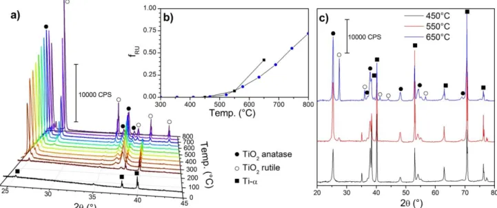
By increasing the annealing temperature of TiO2-NTs samples,
the TiO2 crystalline structure is expected to gradually change
under thermal kinetic control from amorphous titanium oxide to anatase TiO2 and then to rutile phase. In order to determine
the temperature range of these transitions, X ray diffraction pattern of a pristine TiO2-NTs sample was recorded in situ at
different temperatures up to 800°C. The results presented in figure 1.a), exhibit no changes between 50 and 250°C and only the peaks attributed to Ti-α from the metallic foil supporting amorphous nanotubes can be observed (2θ = 25.73, 38.27 and 40.16°). From 300°C the diffraction pattern of anatase appears and the peak intensities increase with temperature. When the temperature reaches 500°C the contribution of rutile phase is observable and increases continuously with temperature until the upper limit of 800°C. The weight fraction of rutile fRu can
be estimated from the area of the (101) reflexion peak of anatase (AA; 2θ = 25.34°) and the (110) peak of rutile (ARu; 2θ =
27.42°) according to the following equation:
(1)
K is a correction factor (0.52) taking into account the relative
sensitivity of the two phases. This factor was determined experimentally by recording XRD patterns of anatase/rutile mixture with known amount of each phase. As observed in figure 1.b), the contribution of rutile increases exponentially from 450 to 800°C and reach a final value of 72% of rutile. It should be noticed that eq.1 was mainly applied for TiO2
powder. In the case of aligned TiO2-NTs grown on Ti foil, there
is preferential crystallographic orientation along the [001] for rutile and [100] for anatase.32 Consequently, the mass proportions measured in our case give a clear tendency but
Figure 1: Temperature dependant X –ray diffraction patterns of TiO2-NTs grown on titanium foil (a) and XRD of the TiO2-NTs samples annealed at the three different
temperatures (c). The fraction of rutile phase depending on temperature for the in situ experiment (blue circles) and for the three samples prepare d for PEC experiments (black squares) is represented (b).
cannot be considered as absolute values. Moreover, the repartition between rutile and anatase is not homogeneous. Indeed according to previous reports, rutile is likely to be formed mainly at the bottom of the tubes, by thermal oxidation of the titanium substrate.30,33 A rutile thickness up to 1 m was determined in a 2m thick TiO2 NTs layer after
annealing at 650 °C.34 We used the Debye-Scherrer method to evaluate the size of the coherent crystalline domains of anatase and rutile from the width of diffraction peaks.35 The results are presented in ESI figure S1b. The crystallite width of anatase increases with the temperature from 15 to 28 ± 2 nm. For rutile, the crystallite size can only be measured above 500°C, when the phase appears and the width increases much faster than for anatase from 10 to 50 nm. The wall thickness of the TiO2-NTs measured by SEM measurement is ranging from
20 to 30 nm. Consequently, the average size of rutile crystallite is only compatible with the bottom of the tubes, were the walls are thicker,36 and accordingly to the literature.29,30,33,34
Figure 2: SEM images of TiO2-NTs samples synthesised at 45V in ethylene glycol based
electrolyte and annealed at 450°C (a), 550°C (b), 650°C (c) and 700°C (d).
Taking in consideration these results, three samples of TiO2-NTS were synthesized in similar anodization conditions
and then annealed at 450°C, 550°C and 650°C to obtain different proportions of anatase and rutile. The minimum temperature of 450°C was chosen to obtain a sample with only anatase phase and the maximal temperature was limited to 650°C since higher temperature results in damaged nanotubes structure because of the volume change between anatase and rutile lattices (Fig. 2.d). The diffraction patterns of these samples are presented in figure 1.c. As expected, no diffraction peaks of the rutile phase appear for the sample annealed at 450°C. The sample annealed at 550°C and 650°C presented a mixture of the two phases, with 7% and 42% of rutile respectively. The deviation in the rutile ratio between the sample and the in situ experiment around 650°C can be explained by different quantity of heat transferred in the two experiments (i.e. steady state versus transient heating; calibration of thermocouple etc...)
The morphology of the TiO2 nanotubes after thermal
treatment was observed by SEM, with an observation angle of 45°, on the edge of the TiO2-NTs layer (Fig. 2). The samples
annealed at three different temperatures (Fig 2.a, b and c) present similar morphology and close dimensions, reported in table 1, with a length around 4 µm. The external and internal diameters (Dout and Din) are around 100 and 50 nm
respectively. The external diameter slightly diminish from 107 ±6 to 93 ±9 nm while the internal one increases when the temperature increase. Consequently the wall thickness decreases from 30 to 21 nm. With this value we are able to calculate a specific surface area for the samples considering the surface developed by the TiO2-NTs packed in a compact
hexagonal arrangement and the density of TiO2.31 The
obtained value of 20 ±3 m2.g-1 is in good agreement with BET measurements conducted with krypton on a TiO2-NTs film
Journal Name ARTICLE
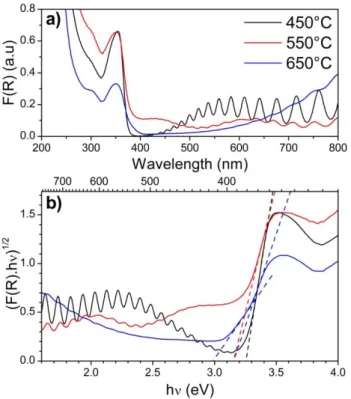
Figure 3: Diffuse reflectance data of the TiO2-NTs samples annealed at 450, 550
and 650°C. (a) Kubelka-Munk function and (b) Tauc plot for bandgap calculation.
UV-visible spectroscopy
The light absorption properties of TiO2-NTs samples annealed
at different temperatures were measured by diffuse reflectance spectroscopy. Figure 3.a represents the Kubelka-Munk function calculated from the reflectance R, according to:37
(2)
The Kubelka-Munk function can be considered as an equivalent of the absorption for thin films materials. In the visible range of the spectra (λ > 400 nm), the NTs film present a non zero absorption that can be explained by two phenomena. First, TiO2-NTS films are annealed with the
titanium foil whose colour changes during the thermal treatment and contribute to the light absorption and explains the difficult baseline subtraction. Secondly, the interference fringes typical of thin film materials can be observed, mainly for the sample at 450°C, they originate from interferences between photons reflecting at the TiO2-NTs surface and those
reflected at the Ti interface after propagating in the film.38 These oscillations indicate the high level of organisation and the homogeneous length of the TiO2-NTs tubes. These
interference fringes can be used to estimate the thickness d of the film from the wavelengths of the peak m (λm) and the peak
m+x (λm+x) according to:
(3) with θ the angle of incidence, na the refractive index of the
incidence medium (na = 1 for air) and nfλ the film refractive
index at a given wavelength. The film refractive index was calculated considering a porosity of 60% and from the value reported for an anatase thin film.39 The thickness calculation was made for the 5 peaks at higher wavelength of each sample and was found to be in good agreement with the SEM measurements with values ranging from 4010 ± 130 nm for the sample annealed at 450°C to 3800 ± 100 nm for the one at 650°C.
The apparent band gap EG of the semi-conductor film was
calculated from the Tauc plot (figure 3.b.) by the intercept of the abscise axis with the straight line defined by equation 4:
(4)
for an indirect bandgap material, like TiO2 anatase, m = 2. A is
a constant whose value is determined by the maximum of the first derivative of Tauc curves. For the TiO2-NTs samples
containing anatase exclusively the bandgap has a value of 3.26 ± 0.05 eV and the samples annealed at 550°C present a slightly reduced EG value of 3.17 ± 0.05 eV. These values are consistent
with the one reported in the literature for anatase TiO2.40 In
the case of the sample annealed at 650°C, two linear domains appear on the Tauc plot (fig. 3.c blue). They correspond to bandgap energies of 3.15 ± 0.05 and 2.99 ± 0.06 eV which can be attributed to anatase and rutile crystallites in the TiO2
nanotubes respectively. The two distinctive bandgaps can be observed only for the sample annealed at 650°C thanks to its high proportion of rutile.
Table 1: Physical Characteristics of the TiO2-NTs samples annealed at different
temperature.
Photo-Electrochemical measurements
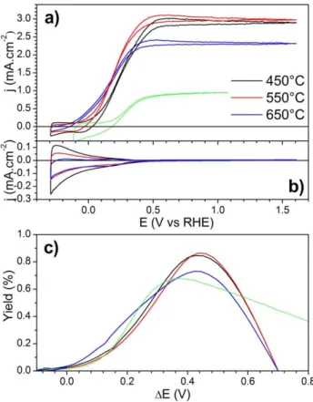
Cyclic voltametry results of the 3 electrodes, recorded under irradiation and in the dark, are presented in figure 4.a and 4.b. The CV exhibit the same shape with the photocurrent increasing for potential higher than 0 V vs RHE and reaching a plateau around 0.5 V. For the samples annealed at 450 and 550°C the maximum photo-current reaches approximately 3.0 mA.cm-2. The higher annealing temperature results in a reduced photo-current of 2.3 mA.cm-2. Additionally, the slope of the curve between 0 and the maximum photo current is slightly reduced indicating a more resistive behaviour of the electrode. For comparison, we added the cyclic voltametry for the sample annealed at 450°C in the absence of methanol. The shape is similar, but the photocurrent is strongly reduced. The higher photocurrent measured in the presence of methanol is explained by the fact that the (photo-)electrocatalytic oxidation of MeOH is an easier reaction than water oxidation (i.e. 2 vs 4 e- process). Consequently, holes are more efficiently used for oxidation, minimizing their recombination with photo-generated electrons.
Anneal Temp. Length (µm) Dout (nm) Din (nm) Eg (eV)
450°C 4.04 ±0.16 107 ±6 47 ±6 3.26
550°C 4.14 ±0.10 98 ±11 48 ±9 3.17
Figure 4: Cyclic voltamograms of TiO2-NTs photo-anodes annealed at 450, 550
and 650°C in 0.2 mol.L-1 NaOH and 0.4 mol.L-1 MeOH (a) under illumination and
(b) in the dark. The data in green are obtain without sacrificial agent for the photo-anode annealed at 450°C. (c) Corresponding ABPE of the 3 electrodes.
From these data the Applied Bias Photon to current Efficiency (ABPE) of each electrode can be calculated to compare the efficiency of the different electrodes according to:41
(5)
with jph the photocurrent, ΔE the bias voltage defined as the
difference between the applied voltage at the working electrode and the open circuit potential of the photo-anode under illumination. Erev is the thermodynamic potential
corresponding to the reaction, namely 1.23 V for water splitting. In the case of MeOH oxidation, the value of 0.7 V reported in the literature for oxidation into CO2 was used.
42
Figure 4.c shows the ABPE of the different electrodes and confirms the best performances of TiO2-NTs thermally treated
at 450 and 550°C.
By using monochromatic irradiation in photo-electrochemical experiments, it is possible to determine IPCE that can be defined as the ratio between the number of collected electrons and the number of incident photons on the cell according to equation 6:
(6)
jph(λ) and P(λ) are the measured photocurrent and the incident
light power density at a given wavelength λ, respectively. IPCE values of the three samples are reported in figure 5. In figure 5.a, one can observe the same tendency than the one
Figure 5: Incident Photon to Electron Conversion Efficiency of the three samples (a),
representation in logarithmic scale of the 300 – 450 nm spectral domain (b) and Tauc plot of the IPCE (c).
observed on cyclic voltametry: the samples annealed at 450 and 550°C present higher conversion efficiency than the one at 650°C and they achieve a quantum yield close to 97 ± 2% at 355 nm. With this IPCE representation all samples appear to absorb in the same spectral domain while on UV-visible spectra the contribution of rutile was observable. On figure 5.b IPCE is represented in logarithmic scale and it is possible to distinguish the small contribution of rutile around 400 nm. At this wavelength the IPCE of the sample annealed at 650°C is 40% higher than the one of the two other samples. The two vertical dashed lines in figure 5.b correspond to the wavelength of the LEDs used for irradiation in IMPS experiments discussed in the last part of the manuscript.
An equivalent of Tauc plot was calculated from IPCE: from these values it is possible to determine a photo-conversion bandgap. Accordingly to what was previously mentioned, only the contribution of anatase appears and we can determine a band-gap of 3.14 ± 0.03 eV for all samples.
In order to check the consistency between CV (full spectrum of Xe lamp) and IPCE (monochromatic irradiation) measurements, the latest is integrated and convoluted with the Xe lamp spectra according to:
Journal Name ARTICLE
PXe(λ) is the power density of the Xe lamp at a given
wavelength. JIPCE is then the value of photocurrent expected
for the Xe lamp at the potential used for IPCE measurements (1V vs RHE). It should be equivalent to the photocurrent measured by CV at the same potential. With JIPCE values of
2.85, 2.90 and 2.29 ±0.05 mA.cm-2, for samples annealed at 450, 550 and 650°C respectively, the difference with cyclic voltametry results is less than 5% confirming the reliability of the different steady state measurements.
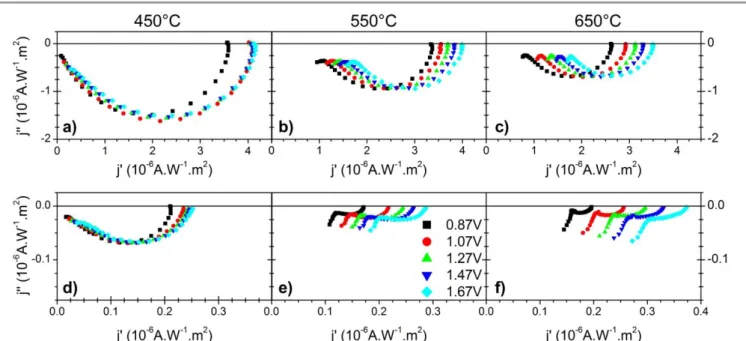
Intensity modulated photocurrent
spectroscopy measurements
IMPS technique combines a strong continuous irradiation with a small sinusoidal modulation of light intensity in order to determine the values of rate constants for charge transfer and recombination.13 IMPS data are presented in figure 6 for the 3 samples measured at 375 and 400 nm at different potentials. It clearly appears that for the sample annealed at 450°C (anatase), the Bode diagrams poorly depend on the applied potential in a wide potential range. On the contrary in the case of rutile containing electrodes, the diagrams show a strong dependence on the applied potential and the evolution is more pronounced when the rutile content increases.
Theoretical models of IMPS have been proposed and successfully applied for different materials.16 In this work, only two elementary steps were considered for the photocurrent: direct charge transfer and recombination (rate constants ktr
and krec, respectively). Within these conditions, the analytical
expression of the ac component of the photocurrent has been derived by Ponomarev et al as following: 15,16
(8)
where Io is the amplitude of the modulated photocurrent, Csc the
space charge layer capacitance, CH the Helmoltz layer capacitance, C
the interfacial capacitance (equation 9)
(9)
Ctrap is an additional contribution of surface states not involved in
recombination and trap = RtrapCtrap. From equation (8) it is seen that
the real part of j() at = 0 tends towards Ioktr/(ktr+krec).
Eq. 8 was used for fitting of the results using the SIMAD software. Two values Rs and Io were fixed, limiting the number of
adjustable parameters to 6. The Rs value was determined previously
from EIS measurements and the Io value was taken at the
low-frequency intercept of the single semicircle at E= 1.77 V vs RHE), at which it is assumed that surface recombination are minimized and can be fully neglected. To check the reliability of the rate constants determined by IMPS, we have verified that for each case the calculated current Ioktr/(ktr+krec) which represents the amplitude of
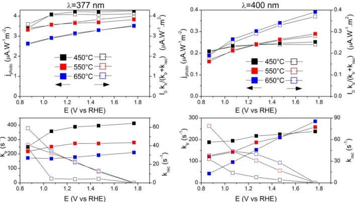
the modulated photocurrent is well proportional to the steady-state photocurrent jphoto. As represented in figure 7.a and b, for
both illumination wavelengths close values are obtained. The evolutions of ktr (charge transfer rate), krec (recombination rate) as a
function of applied potential are reported in Figure 7.c and d, for the three annealing temperatures and the two wavelengths. For the anatase sample, the transfer rate constant ktr presents a plateau for
potentials positive to 1.07 V vs RHE), in agreement with the photocurrent plateau. The value of the plateau decreases when the rutile content increases. Under sub-bandgap illumination, ktr
increases linearly with potential, the higher the slope, the higher the rutile content. The recombination rate constant krec presents a
decreasing exponential behavior with potential in the different cases. The variations of Csc with potential were analyzed on the
basis of the previously developed electrical model taking into account the nanotubular geometry] providing an estimation of the carrier density (5.1019 cm-3) and of the flat band potential Efb = +
0.37 0.05 V vs RHE (Not shown).43
Figure 7: Data treatment of IMPS measurement at 377 (a, c) and 400 nm (b, d). Steady state photocurrent and I0 ktr/(ktr+krec) ratio as a function of the applied
potential (Figure 7.a and b); evolution of ktr and krec for the TiO2-NTs annealed at 450, 550 and 650°C (figure 7.c and d.) At wavelength close to the band gap value (377 nm), only the
outermost part of the NT layer is absorbing light, consequently, the photogenerated charges are created in this zone. Holes are collected at the surface of the tubes while electrons are diffusing to the back contact. The space charge layer which is situated in the wall region of the tube gets progressively depleted with increasing bias. Due to the short diffusion path of holes in the tube wall (half the wall width, between 15 and 10 nm in the present case), saturation of the photocurrent is expected already at a relatively small bias. This is clearly observed in the sample annealed at 450°C (Fig 7.a) at potentials positive to 1.07 V vs RHE. Another consequence of the short diffusion path of holes in NT layers is that the hole transfer is a very fast process. The rate constant ktr is then
likely to concern mainly electron transfer towards the back contact.
krec provides a global description of the surface recombination
kinetics betweenphotogenerated charges, with an exponential but non ideal behaviour with the applied potential E. The recombination rates krec are found to be proportional to
exp[-e(E-Efb)/(mkBT)] with m much larger than unity, the larger is m,
the higher is the annealing temperature. This is due to the difference of trapping level energy in anatase and in rutile phases: anatase presents shallow trap levels, while rutile shows deeper traps, slowing down the electron transfer by hopping process.17,24 This is reflected by comparing the values of IPCE at 377 nm with the evolution of the ktr at 377 nm. ICPE values are 0.240, 0.214 and
0.202 for samples annealed at 450, 550 and 650°C respectively, corresponding to a decrease of 15% when the annealing temperature is increased. A similar decrease is observed for jphoto,
but at the same time ktr is reduced by 50% from 400 s-1 and 200 s-1.
This observation suggests that almost the same quantities of photon are absorbed by the TiO2-NTs (mainly at their surface) to
generate electrons, but the increasing amount of rutile present at the bottom of the nanotubes slows down their transport towards the back contact. Furthermore it can be noted that when the amount of rutile increases, ktr is less and less depending on the
applied potential. This suggests that the electron transport in that case will not depend on the collection in the space charge layer, but is mainly limited by the conductivity of the rutile fraction at the bottom of the nanotubes.
The photoconversion efficiency of TiO2–NTs at 400 nm is
strongly reduced when compared to the one at 377 nm, whatever the annealing temperature. Nevertheless, the activity stays 50% higher in rutile rich sample (Fig 5). Since the penetration depth of light increases and anatase absorbs less photons than rutile at this wavelength, charge carriers are likely to be generated in rutile located at the bottom of the NTs film. In Fig 7.d, the evolution of ktr
for the pure anatase sample at 400 nm exhibits a poor dependence on the applied potential. It is noticeable that ktr value is strongly
reduced at 400 nm when compared to 377 nm values (from 400 s-1 to 200 s-1). This can be explained by the lower light absorption at 400 nm: less photo-generated electrons are available to fill the trapping levels in anatase and consequently the conductivity of NTs by hopping process decreases.22 When the rutile ratio increases, the potential dependence of ktr is more and more obvious. For the
sample annealed at 650 °C, in which rutile phase is dominant, ktr
has a linear dependence on potential, passing from 40 to 300 s-1. It even reaches a higher value than for anatase when the applied potential increases. This linear dependence of ktr with potential can
be correlated with a possible potential distribution along the tubes due to the increased material resistivity. Considering the linear variation of the steady state photocurrent with potential a rough estimate of the corresponding resistance would be about 3 kcm2.
Journal Name ARTICLE
Conclusions
Different characterization methods were used to study the influence of the annealing temperature on the crystalline and photo-electrochemical properties of TiO2-NTs obtained by
anodization. Temperature dependent X ray diffraction allowed us to identify the transition between amorphous, anatase and rutile phase and to estimate the amount of each phase in the different nanotube films. Optical spectroscopy was used to determine how the amount of rutile in the sample affects the optical bandgap. It evolved from 3.26 to 2.99 eV when the amount of rutile increased. In the case of sample annealed at 650°C, identified as the high temperature limit for a stable nanotubular structure, two different bandgaps appeared at 3.15 and 2.99 eV that were attributed respectively to distinctive anatase and rutile domains.
These different samples were characterized by photo-electrochemical methods, showing that the performance of the TiO2-NTs electrode decreases for high ratio of rutile in the
nanotubes. The PEC spectral responses of the different electrodes were measured by ICPE indicating no specific changes in the photoconversion, with a apparent band gap value of 3.14 eV, whatever the annealing temperature. A closer look on the IPCE data around 400 nm shows a small improvement of the photo-conversion efficiency due to the presence of rutile.
To further study this aspect, frequency dependent photo-electrochemical method was used. By measuring the IMPS response at two different wavelengths of irradiation it was possible to highlight the influence of rutile on the charge transfer in TiO2-NTs layer. Given that the rutile phase is located
at the bottom of the tubes and given the difference of light absorption between anatase and rutile phases, by using irradiation at 377 nm mainly the anatase phase at the top of the nanotubes photogenerate charge carriers. On the contrary at 400 nm which allows deeper penetration of light, the overall photo-electrochemical response is dominated by the rutile. The main conclusions from IMPS experiments emphasize that in the different situations, the value of the photocurrent is directly determined by the rate of electron transport towards the metallic substrate. When the amount of rutile increases an additional resistance at the bottom of the tubes lowers the transfer rate.
The present work shows that IMPS operated with several excitation sources is a powerful tool for characterizing spatially distributed biphasic photo-electrochemical systems and to provide information about photogenerated charge carrier transport properties in such a nanostructured semi-conductors layers.
Acknowledgements
This work was funded by the University of Strasbourg through an IdEX project (CoDoTiN) and ANR JCJC program (BAGETE). Thierry Dintzer and Thierry Romero are gratefully acknowledged for the XRD and SEM measurements.
Notes and references
1 N. S. Lewis, M. G. Walter, E. L. Warren, J. R. McKone, S. W. Boettcher, Q. Mi and E. A. Santori, Chem. Rev., 2010, 110, 6446– 6473.
2 S. U. M. Khan, M. Al-Shahry and W. B. Ingler Jr., Science, 2002,
297, 2243–2245.
3 F. E. Osterloh, Chem Soc Rev, 2013, 42, 2294–2320.
4 P. Schmuki, K. Lee and A. Mazare, Chem. Rev., 2014, 114, 9385– 9454.
5 T. Cottineau, N. Béalu, P.-A. Gross, S. N. Pronkin, N. Keller, E. R. Savinova and V. Keller, J. Mater. Chem. A, 2013, 1, 2151.
6 J. J. Brancho and B. M. Bartlett, Chem. Mater., 2015, 27, 7207– 7217.
7 M. Kapilashrami, Y. Zhang, Y.-S. Liu, A. Hagfeldt and J. Guo,
Chem. Rev., 2014, 114, 9662–9707.
8 K. Sivula and R. van de Krol, Nat. Rev. Mater., 2016, 1, 15010. 9 A. Murphy, P. Barnes, L. Randeniya, I. Plumb, I. Grey, M. Horne and J. Glasscock, Int. J. Hydrog. Energy, 2006, 31, 1999–2017. 10 L. M. Peter, Electroanalysis, 2015, 27, 864–871.
11 Y. Tamaki, A. Furube, M. Murai, K. Hara, R. Katoh and M. Tachiya, Phys. Chem. Chem. Phys., 2007, 9, 1453.
12 Y. Yamada and Y. Kanemitsu, Appl. Phys. Lett., 2012, 101, 133907.
13 L. M. Peter, J. Solid State Electrochem., 2013, 17, 315–326. 14 L. M. Peter, K. G. U. Wijayantha and A. A. Tahir, Faraday Discuss, 2012, 155, 309–322.
15 H. Cachet and E. M. M. Sutter, J. Phys. Chem. C, 2015, 119, 25548–25558.
16 E. A. Ponomarev and L. M. Peter, J. Electroanal. Chem., 1995,
396, 219-226.
17 R. P. Lynch, A. Ghicov and P. Schmuki, J. Electrochem. Soc., 2010, 157, G76.
18 Y. Ma, X. Wang, Y. Jia, X. Chen, H. Han and C. Li, Chem. Rev., 2014, 114, 9987–10043.
19 S. Banerjee, D. D. Dionysiou and S. C. Pillai, Appl. Catal. B
Environ., 2015, 176–177, 396–428.
20 A. Yamakata, J. J. M. Vequizo and H. Matsunaga, J. Phys. Chem.
21 P. Salvador, J. Appl. Phys., 1984, 55, 2977–2985.
22 T. Luttrell, S. Halpegamage, J. Tao, A. Kramer, E. Sutter and M. Batzill, Sci. Rep., , DOI:10.1038/srep04043.
23 D. Reyes-Coronado, G. Rodriguez-Gattorno, M. E. Espinosa-Pesqueira, C. Cab, R. de Coss and G. Oskam, Nanotechnology, 2008,
19, 145605.
24 B. Moss, K. K. Lim, A. Beltram, S. Moniz, J. Tang, P. Fornasiero, P. Barnes, J. Durrant and A. Kafizas, Sci. Rep., , DOI:10.1038/s41598-017-03065-5.
25 J. R. Jennings, A. Ghicov, L. M. Peter, P. Schmuki and A. B. Walker, J. Am. Chem. Soc., 2008, 130, 13364–13372.
26 C. B. Marien, T. Cottineau, D. Robert and P. Drogui, Appl. Catal.
B Environ., 2016, 194, 1–6.
27 X. Zhang, K. Huo, L. Hu, Z. Wu and P. K. Chu, J. Am. Ceram. Soc., 2010, 93, 2771–2778.
28 D. A. H. Hanaor and C. C. Sorrell, J. Mater. Sci., 2011, 46, 855– 874.
29 S. P. Albu, H. Tsuchiya, S. Fujimoto and P. Schmuki, Eur. J. Inorg.
Chem., 2010, 2010, 4351–4356.
30 S. Das, R. Zazpe, J. Prikryl, P. Knotek, M. Krbal, H. Sopha, V. Podzemna and J. M. Macak, Electrochimica Acta, 2016, 213, 452– 459.
31 J. M. Macak, S. P. Albu and P. Schmuki, Phys. Status Solidi RRL –
Rapid Res. Lett., 2007, 1, 181–183.
32 P. Acevedo-Peña, F. González, G. González and I. González, Phys
Chem Chem Phys, 2014, 16, 26213–26220.
33 A. Tighineanu, S. P. Albu and P. Schmuki, Phys. Status Solidi RRL
- Rapid Res. Lett., 2014, 8, 158–162.
34 S. Ozkan, A. Mazare and P. Schmuki, Electrochimica Acta, 2015,
176, 819–826.
35 J. I. Langford and A. J. C. Wilson, J. Appl. Crystallogr., 1978, 11, 102–113.
36 T. Cottineau, S. N. Pronkin, M. Acosta, C. Mény, D. Spitzer and V. Keller, Sens. Actuators B Chem., 2013, 182, 489–497.
37 P. Kubelka, JOSA, 1948, 38, 448–448.
38 G. L. Chiarello, A. Zuliani, D. Ceresoli, R. Martinazzo and E. Selli,
ACS Catal., 2016, 6, 1345–1353.
39 A. Bendavid, P. J. Martin and H. Takikawa, Thin Solid Films, 2000, 360, 241–249.
40 D. O. Scanlon, C. W. Dunnill, J. Buckeridge, S. A. Shevlin, A. J. Logsdail, S. M. Woodley, C. R. A. Catlow, M. J. Powell, R. G. Palgrave, I. P. Parkin, G. W. Watson, T. W. Keal, P. Sherwood, A. Walsh and A. A. Sokol, Nat. Mater., 2013, 12, 798–801.
41 Z. Chen, T. F. Jaramillo, T. G. Deutsch, A. Kleiman-Shwarsctein, A. J. Forman, N. Gaillard, R. Garland, K. Takanabe, C. Heske, M. Sunkara, E. W. McFarland, K. Domen, E. L. Miller, J. A. Turner and H. N. Dinh, J. Mater. Res., 2010, 25, 3–16.
42 T. Iwasita, Electrochimica Acta, 2002, 47, 3663–3674.
43 P. Pu, H. Cachet, E. Ngaboyamahina and E. M. M. Sutter, J. Solid