Publisher’s version / Version de l'éditeur:
Optics Express, 17, 8, pp. 6655-6664, 2009
READ THESE TERMS AND CONDITIONS CAREFULLY BEFORE USING THIS WEBSITE. https://nrc-publications.canada.ca/eng/copyright
Vous avez des questions? Nous pouvons vous aider. Pour communiquer directement avec un auteur, consultez la
première page de la revue dans laquelle son article a été publié afin de trouver ses coordonnées. Si vous n’arrivez pas à les repérer, communiquez avec nous à [email protected].
Questions? Contact the NRC Publications Archive team at
[email protected]. If you wish to email the authors directly, please see the first page of the publication for their contact information.
NRC Publications Archive
Archives des publications du CNRC
This publication could be one of several versions: author’s original, accepted manuscript or the publisher’s version. / La version de cette publication peut être l’une des suivantes : la version prépublication de l’auteur, la version acceptée du manuscrit ou la version de l’éditeur.
For the publisher’s version, please access the DOI link below./ Pour consulter la version de l’éditeur, utilisez le lien DOI ci-dessous.
https://doi.org/10.1364/OE.17.006655
Access and use of this website and the material on it are subject to the Terms and Conditions set forth at
Interferometric sensing platform with dielectric nanostructured thin
films
Celo, D.; Post, E.; Summers, M.; Smy, T.; Brett, M. J.; Albert, J.
https://publications-cnrc.canada.ca/fra/droits
L’accès à ce site Web et l’utilisation de son contenu sont assujettis aux conditions présentées dans le site LISEZ CES CONDITIONS ATTENTIVEMENT AVANT D’UTILISER CE SITE WEB.
NRC Publications Record / Notice d'Archives des publications de CNRC:
https://nrc-publications.canada.ca/eng/view/object/?id=97768a82-5418-4661-92d5-25c05a3d586e https://publications-cnrc.canada.ca/fra/voir/objet/?id=97768a82-5418-4661-92d5-25c05a3d586eInterferometric sensing platform with dielectric
nanostructured thin films
D. Celo1*, E. Post2, M. Summers3, T. Smy1, M.J. Brett3, and J. Albert1
1Carleton University, Department of Electronics, 1125 Colonel By Drive,
Ottawa, ON, K1S 5B6 Canada
2The Institute for Microstructural Sciences, National Research Council,
Ottawa, ON, Canada K1A 0R6
3National Institute for Nanotechnology, National Research Council,
Edmonton, AB, Canada T6G 2M9 * Corresponding author: [email protected]
Abstract: A new interferometer-based optical sensing platform with
nanostructured thin films of ZrO2 or TiO2 as sensing environment has been
developed. With the application of an IC compatible Si3N4 waveguide
technology, Mach-Zehnder interferometer devices have been fabricated. The application of the glancing angle deposition technique allowed fabrication of nanostructured thin films as the optical sensing environment. Sensing ability of fabricated devices has been demonstrated through the refractive index measurement of a known gas. The transmission spectra and time response measurements have demonstrated a maximum phase shift of φ=π/10 and a | Pout|=0.65 dBm. Devices with TiO2 film on the sensing
region performed much better than devices with ZrO2, with sensitivity twice
as high.
©2009 Optical Society of America
OCIS codes: (130.0130) Integrated optics; (130.6010) Sensors
References and links
1. P. V. Lambeck, “Integrated optical sensors for the chemical domain,” Meas. Sci. Technol. 17, R93-R116 (2006).
2. L. M. Lechuga, F. Prieto, and B. Sepulveda, in Optical Sensors for Industrial and Environmental
Applications, (Springer, 2003).
3. J. van Lith, P. V. Lambeck, J. W. Hoekstra, R. G. Heideman, and R. R. Wijn, “The segmented waveguide sensor: principle and experiments,” J. Lightwave Technol. 23, 355-363 (2005).
4. S. Létant and M. J. Sailor, "Detection of HF gas with a porous Si interferometer," Adv. Mater. 12, 355-359 (2000).
5. K. Robbie, L .J. Friedrich, and S. K. Dew, “Fabrication of thin films with high porous nanostructure,” J. Vac. Sci. Technol. A 13, 1032-1035 (1995).
6. J. Steele, A. van Popta, M. Hawkeyea, J. Sit, and M. Brett, “Nanostructured gradient index optical filter for high-speed humidity sensing,” Sens. and Actuators B 120, 213–219 (2006).
7. K. Harris, A. Huzinga, and M. Brett, “High-speed porous thin film humidity sensors,” Electrochem. Solid-State Lett. 5, H27– H29 (2002).
8. S. Hsu and Y. Huang, “A novel Mach-Zehnder interferometer based on dual arrow structures for sensing applications,” J. Lightwave Technol. 23, 4200–4206 (2005).
9. R. N. Fabricius, G. Gauglitz, and J. Ingenhoff, “A gas sensor based on an integrated optical Mach-Zehnder interferometer,” Sens. and Actuators B, 7, 672-676 (1992).
10. R. Ramaswami and K. N. Sivarajan, in Optical Networks: A Practical Perspective, Second ed., (Morgan Kaufmann, 2002).
11. G. J. Valdhuis, O. Parriaux, H. J. Hoekstra, and P. V. Lambeck, “Sensitivity enhancement in evanescent optical waveguide sensors,” J. Lightwave Technol. 18, 677-682 (2000).
12. Optiwave, "Waveguide Optics Modeling Software Systems," in OptiBPM Technical Background, Ottawa, ON, Canada, (2005).
13. A. Dakka, J. Lafait, C. Sella, S. Berthier, J. C. Martin, and M. Maaza, “Optical properties of Ag–TiO2 nanocermet films prepared by cosputtering and multilayer deposition techniques,” Appl. Opt. 39, 2745-2753 (2000).
14. M. W. McCall and A. Lakhatakia, “Integrated optical polarization filtration via sculptured-thin-film technology,” J. Mod. Opt. 48, 2179-2184 (2001).
15. B. Dick and M. J. Brett, “Nanofabrication by glancing angle deposition,” Encyclopedia of Nanoscience and Nanotechnology, 6, 703-725 (2004).
16. D. Celo, R. Vandusen, T. Smy, J. Albert, N. G. Tarr, and P. D. Waldron, “Low temperature plasma etching for Si3N4 waveguide applications,” J. Vac. Sci. Technol. A 26, 253-258 (2008).
17. A. C. van Popta, J. Cheng, J. C. Sit, and M. J. Brett, “Birefringence enhancement in annealed TiO2 thin
films,” J. Appl. Phys. 102, 013517 (2007).
18. G. Gulen and M. N. Inci, “Thermal optical properties of TiO2 films,” Opt. Mater. 18, 373-381 (2002).
19. E. Drouard, P. Huguet-Chantome, L. Escoubas, and F. Flory, “ n/ T measurements performed with guided waves and their application to the temperature sensitivity of wavelength-division multiplexing filters,” Appl. Opt. 41, 3132-3136 (2002).
20. E. Hecht, Optics, (Addison Wesley Longman, Inc., Third ed., 1998).
1. Introduction
During the last decade, a need for faster and better means of detection, communication, and data processing has encouraged rapid growth on the field of all-optical components. This has led to the development of a variety of new optical sensing devices able to detect a measurand and process data using electromagnetic energy. From the wide range of integrated optical sensors, devices based on interferometric homogenous sensing have been successfully developed [1]. While some good sensitivities are reported[2, 3], there are limiting factors inherited to the existing methodology of device design and fabrication. A large refractive index difference at the waveguide core-measurand boundary causes: (a) the mode propagating into the waveguide to be strictly confined inside the core region, resulting in a very small evanescent field portion, (b) the evanescent field traveling into the sensing area experiences high absorption and scattering losses, and (c) increases Fresnel reflection losses at the boundaries, leading to a potential interference of the reflected power with the evanescent filed. A possible solution to these problems would be a sensing environment with strictly controlled refractive index, porosity, structural configuration and high surface area to volume ratio. While similar structures using porous materials have been fabricated from other research groups [4], the application of thin films fabricated with the glancing angle deposition (GLAD) technique [5] offers a high degree of control over the film nanostructure. The porous nature of sensing layer makes the device sensitive to the voids environment; as it propagates along the film, the evanescent field drawn deep into the porous layer probes the environment. The limited interaction of the evanescent field with the sensitive cladding is compensated by the long propagating distance. Furthermore, this technology allows the development of a so-called sensor platform [1], which with minor modifications can be tailored to a large variety of optical sensing devices. By changing very few deposition parameters such as flux incidence angle or angular velocity of substrate rotation, a broad range of nanostructured thin films (NTF) specific to individual applications can be created [6, 7].
The capability of the proposed sensing platform for refractive index measurement is demonstrated in this work. The design aspects briefly address the rationale behind the use of interferometric sensing with a Mach-Zehnder interferometer (MZI). The effect of core-cladding refractive index on the modal sensitivity is simulated, with results suggesting that good optical sensitivity can be achieved with devices based on silicon nitride (Si3N4)
waveguides and zirconia (ZrO2) or titania (TiO2) NTF deposited on the sensing region.
Processing and fabrication section summarizes waveguide fabrication steps and the application of GLAD technology for deposition of dielectric NTFs of slanted columns. Finally, the optical sensing ability of fabricated devices is demonstrated through the refractive index measurement of a known gas.
2. Design considerations
The advantage of the MZI in various interferometric sensing applications [8, 9] is based on the ability to control the optical path difference between arms by changing the refractive index
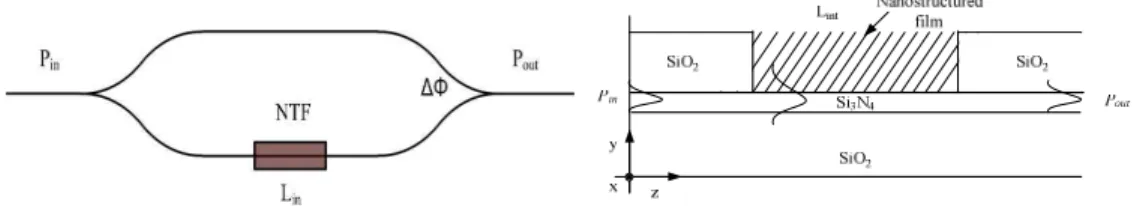
in one of them. Any refractive index change in one arm will strongly affect the output intensity. As schematically shown in Fig. 1, by locally removing the cladding layer in the sensing region, an interaction between the evanescent field of propagating mode and the material to be sensed can be achieved.
Fig. 1. Schematic representation of interferometric sensing (a) a MZI with sensing region in the lower arm, and (b) a magnified sectional view of sensing region depicting waveguide layers and NTF deposited on the opening.
For a single mode condition in the waveguide, the transfer function of the MZI can be seen as a sinusoidal function of φ [10], with the quadrature points occurring when the phase difference between the two arms of the interferometer is φ =(m+1/2)π, for m=0,1,2,... For a given transfer function of a MZI, the effective refractive index change Neff induced by the
refractive index change within the evanescent field region can be obtained with:
eff N L = int 0 2 λ π ϕ (1)
where λ0is the wavelength of light in free space and Lint is the interaction length as shown in
Fig. 1. With this relation, the actual Neff can be estimated by measuring the change in the
fringe period of MZI transfer function. Similarly, Eq. (1) can be used to approximate the actual path length difference in between arms of an unbalanced MZI.
It is generally assumed that the sensitivity of a guided wave to changes of the cladding index is smaller or much smaller than that of a free-space beam [11]. This is based on the fact that only a small fraction of the optical field guided in the waveguide propagates in the sensing medium. In this context, the modal sensitivity (Sm) can be defined as the ratio of the
effective refractive index change of the guided mode to the refractive index change ( nSL) of
the cladding layer.
SL n eff N m S = (2)
Using a mode solver[12], the guided mode effective index of a Si3N4 rib waveguide with
refractive index n=1.92 and thickness t=1 m, and SiO2 buffer of n=1.46 and t=3.5 m was
simulated for a range of sensing layer refractive index values, with results plotted in Fig. 2. As the graph shows, higher sensitivities can be achieved when core-cladding refractive indices get closer; of course, it becomes easier to pull the evanescent field outside the core layer deep into the cladding, where very little change in the cladding refractive index would strongly affect the field distribution inside the waveguide. Therefore a problem arises when we attempt to measure small refractive index changes in low index media (gases and aqueous liquids). With NTFs however, it is possible to achieve high index “average” cladding index, even with porous structures that can be infiltrated by substances to be measured. Small core-cladding refractive index difference can be achieved with ZrO2 and TiO2 NTF deposited on
the sensing layer. Their relatively high refractive index, low absorption coefficient and a high transparency in the visible and near-IR region [13] make these dielectric materials suitable for the purpose.
1.6 1.65 1.7 1.75 1.8 1.85 1.9 1.83 1.84 1.85 1.86 1.87 1.88 Nef f nSL 1.6 1.65 1.7 1.75 1.8 1.85 1.9 0.08 0.16 0.24 0.32 0.4 S
Fig. 2. Waveguide effective refractive index as function of cladding refractive index and simulated modal sensitivity.
The application of the GLAD technique for film deposition makes possible a strict control of optical properties [14], refractive index, porosity, structural configuration and high surface area to volume ratio. As shownin Ref. [5], this technique offers a high degree of control over the film microstructure. Porosity is created by enhanced self-shadowing during the growth process where a random growth fluctuation in one area produces a shadowed region where subsequent incident flux cannot reach and a high point where incident flux may deposit, creating preferred growth. By producing a symmetrical and highly oblique incident flux, shadowing can be greatly enhanced and highly porous films can be fabricated with vertical columns and porosities much greater than those fabricated with a one sided flux [15].
3. Fabrication
The procedure developed in Ref. [16] was adopted to fabricate Si3N4 waveguides and MZI
devices with cross sectional dimensions and refractive indices shown in Fig. 3(a). A theoretical optimization completed on three layer stacks built from SiO2 (n=1.456), Si3N4
(n=1.923) and gas (n in the range 1.0000-1.0010) have shown that the highest sensitivity parameter (Sm=0.0727) at wavelength λ=1.6 m is obtained for a core layer thickness of 239
nm. At calculating the sensitivity such a layer stack is a good approximation for a channel waveguide with small etching depth, leading to the assumption that the application of a porous TiO2 film will improve the device sensitivity. However, it should be noted that the cross
sectional core dimensions of the chosen structure of Fig. 3(a) were not optimized for the highest sensitivity. The main criteria in selecting the core dimensions were the single mode behavior at wavelength 1620 nm and the mode confinement into the rib and evanescent part of the waveguide.
The layer thicknesses with corresponding refractive indices of a typical starting wafer are summarized in Table 1. After waveguide rib formation [Fig. 3(b)], a SiO2 over-cladding layer
of thickness 1.8 m was deposited. Deposition was completed at low temperature (T=500°C) with atmospheric pressure chemical vapor deposition (APCVD) process in a conventional furnace with SiH4 gas and O2 oxidant.
Etching the SiO2 over-cladding to create sensing wells was the next step in the process.
Sensing windows for subsequent NTF deposition were patterned, with openings of size 24 m wide by 2-4 mm long aligned with one of the arms of the balanced MZIs. Wet etching with siloxide etchant was applied, giving the necessary etch control for deposited SiO2 films. It
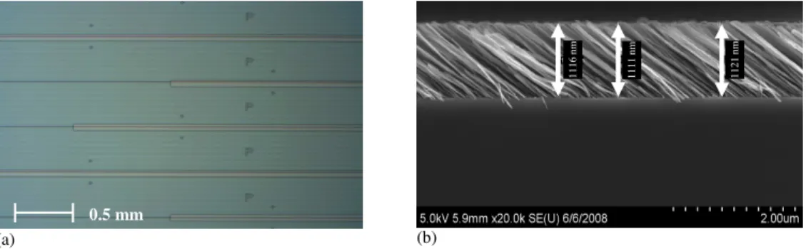
offers: (a) isotropic etching, avoiding vertical steps in the sensing wells, thus allowing a columnar film to be deposited, and (b) high etch selectivity of oxide over mask material and the underlying nitride. A microscope image of an etched wafer depicting sensing regions of three different lengths is shown in Fig. 4(a).
(a) (b)
Fig. 3. The waveguide rib structure (a) a cross-sectional schematic representation, and (b) SEM image of a fabricated waveguide, showing the Si3N4 rib before deposition of SiO2 cladding.
Table 1. Starting wafer parameters
Parameter SiO2 buffer Si3N4 SiO2 cladding
t (nm) 3510 1022 1830
n (λ=650 nm) 1.471 1.947 1.448
n (λ=1551 nm) 1.456 1.923 1.437
The NTF deposition process of source materials (99.7% pure ZrO2 and 99.9% pure Ti3O5
supplied by Cerac Inc.) was completed onto unheated stationary processed wafers. The source to substrate distance of 43 cm and the flux incidence angle set at 85.0±0.1° resulted in porous films with tilted columns at β=45° with the wafer surface, pore volume fraction of 66 %, and refractive indices 1.44 and 1.51 corresponding to ZrO2 and TiO2. An image of a TiO2 film of
thickness 1.12 m deposited on a stationary wafer was taken with a Hitachi S-4800 field emission scanning electron microscope (FE-SEM), and is shown in Fig. 4(b).
(a) (b)
Fig. 4. Sensing windows and TiO2 thin film structure (a) microscope image of a processed
wafer depicting sensing windows where, SiO2 layer has been etched, and (b) SEM image of a
typical film deposited onto stationary processed wafer.
Evaporated thin films of both materials tend to be oxygen deficient. Previous studies [17] have found that an annealing process at a low temperature for an extended period improves film optical properties and crystalline structure. For this reason, deposited films were oxidized in a furnace for 12 hours at 100°C.
Therefore, after completing all the fabrication steps, the final sensor structure is similar to the MZI schematically shown in Fig. 1, where NTF of ZrO2 or TiO2 with thickness 1.1 m
and 45° tilted columns, similar to Fig. 4(b), are deposited in the sensing window of length 3.6 mm. As a result, such sensing devices are considered in the following measurements.
1 m 1 1 1 6 n m 1 1 1 1 n m 1 1 2 1 n m 0.5 mm
4. Experimental setup
A schematic of the measurement setup is shown in Fig. 5. An Agilent Lightwave Measurement System 8164B with tunable laser source module 81600B 200 was used as the light source. The signal from the laser source is transmitted through a single mode polarization-maintaining (PM) fiber into a polarization rotator controller which manipulates and controls the state of polarization of the input beam of light and couples the adjusted light into an output fiber. This polarization controller consisted on three components, a polarizing glass filter for transverse electric (TE) or transverse magnetic (TM) polarized light output, a half-wave plate, and an output coupler with fiber pigtail. The half wave plate position is controlled by a universal motor controller/driver (ESP 300 by NewPort) via a stepper motor, to allow precise and repeatable polarization rotation for TE or TM selection. It also allows the alignment of light as closely to the proper PM fiber axis as possible, thus maintaining the state of linear polarization and orientation of light along one of principal transmission axes within the output fiber.
A single mode PM tapered fiber was used to transmit the linearly polarized optical signal from polarization controller output into the device under test (DUT). Butt-coupling of fiber end to the waveguide facet provides good efficiency and mode matching ability, ensuing minimum coupling losses. The output light from the sample is collected using a 20x objective lens and passed through an analyzer consisting of a broad-band polarizer and a polarizing cube beam-splitter which splits the beam into two orthogonal, linearly polarized components. The output power is directed and measured with an Agilent 81624B InGaAs detector, or reflected (through a mirror) to an infra-red camera for visual inspection and alignment facilitation. The position of the input tapered fiber and the output lens can be controlled with individual stages, whereas the sample can securely be placed in a vacuum controlled stage, providing steadiness during the measurement process. Wavelength and/or time response measurements were run by LabView software.
Fig. 5. Optical measurement setup at NRC optical testing laboratory.
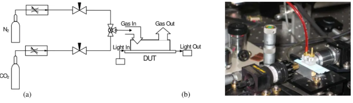
In addition to the optical measurement system, a gas flow system able to create a gas environment surrounding the sensing arm of the MZI was created. A schematic of the gas flow system utilized to measure the refractive index of a known gas is shown in Fig. 6(a). To control the gas environment surrounding the MZI sensing arm, an acrylic cell with dimensions 10x15x10 mm3 was attached to the chip surface [Fig. 6(b)], with a double sided adhesive tape. A gas leak test completed on a dummy silicon wafer demonstrated the capability of this attachment method. Flexible tubing connected to the input hose barb on the gas cell supplied gas inside the cell. Gas flow control was achieved with a three port switch, a needle valve, and a pressure regulator connected at each gas line, permitting identical flow rates for both gasses. Gas cylinders of compressed nitrogen 99.998% purity (reference gas) and carbon dioxide 99.995% purity supplied the gas to the cell.
N2
CO2
DUT
Light In Light Out
Gas Out Gas In
(a) (b)
Fig. 6. Experimental setup for N2 and CO2 refractive index measurement (a) schematic
representation of the system, and (b) photographed image of a waveguide substrate with an acrylic gas cell attached to the surface.
Before completing any optical measurement, the temperature change inside the cell due to the gas flow was measured. A type K thermocouple probe from OMEGA Corp. of diameter 0.25 mm was inserted inside the cell through the output barb. Thermocouple wires were connected to the hand-held unit (OMEGA HH802U), allowing temperature readings as gas flows inside the cell. Air temperature inside the cell with and without gas flow was measured, revealing a maximum temperature difference Tmax≤0.2°C. With thermo-optic coefficients
∂n/∂T=-(1.77±0.7)10-4 K-1 [18] for TiO2 and ∂n/∂T=(3±0.5)10-5 K-1 [19] for ZrO2, the change
in effective refractive index due to temperature is expected to induce a maximum phase shift φ=0.01π. Therefore, the maximum shift in the interferometer output spectrum induced by the thermal variations in the measuring environment is significantly lower than the shifts predicted by simulation results, demonstrating that the gas flow does not change the ambient temperature significantly and therefore cannot be held responsible for the measured changes shown below. This conclusion is further supported by the presence of the Si substrate; its high thermal conductivity provides a good heat sink, thus contributing to a uniform temperature distribution in the MZI arms.
5. Results and discussion
As the gas flows into the cell, the environment surrounding the sensitive layer changes accordingly, resulting in a refractive index change within the evanescent field region. With relation of Eq. (1), the refractive index change affects the Neffand induces a phase shift φ in
the MZI transfer function. As a result, the transfer function Pout=f(λ), will shift accordingly,
reflecting any change in the sensing environment. Measuring this φ after introducing a new gas into the cell gives the ability to determine n and gas refractive index.
Measurements were completed on fabricated devices with ZrO2 or TiO2 NTF deposited in
the sensing window. The gas content into the cell was alternated from N2 (the reference) to
CO2 in five minute intervals and transmittance for TE polarized light was measured at each
interval. A least squares regression procedure to fit a mathematical expression for the transmission power of an unbalanced MZI and the filtered experimental modulation waveform was completed with results shown in Fig. 7. Fitting parameters such as the square of the correlation coefficient (R2) and the chi-square distribution (Chisq) are summarized in Table 2. The wavelength response of the MZI is shifted due to gas content change in the sensing environment. At temperature 0°C and pressure 1 atm the difference in refractive index between N2 and CO2 is approximately n=1.57e-4 refractive index units (RIU) [20]. Since
both gases undergo the same temperature increase, this n is expected to be true even at room temperature, when the measurements were completed. Due to this n, the output intensity of the MZI shifts by π/16 and π/10 respectively for devices with ZrO2 and TiO2.
1580 1590 1600 1610 1620 1630 1640 -20 -18 -16 -14 -12 -10 -8 λ (nm) Po u t ( d B m ) Exp. N2 Exp. CO2 Fitting N2 Fitting CO2 1580 1590 1600 1610 1620 1630 1640 -20 -18 -16 -14 -12 -10 -8 λ (nm) Po u t ( d B m ) Exp. N2 Exp. CO2 Fitting N2 Fitting CO2 (a) (b)
Fig. 7. Output power of MZI with N2 and CO2 in sensing environment for (a) device with ZrO2,
and (b) device with TiO2 film deposited on the sensing arm.
Table 2. Fitting parameters for graphs of Fig. 7.
Device Gas environment R 2 Chisq ZrO2 N2 0.9943 0.1367 CO2 0.9942 0.0871 TiO2 N2 0.9958 0.6347 CO2 0.9977 0.5594
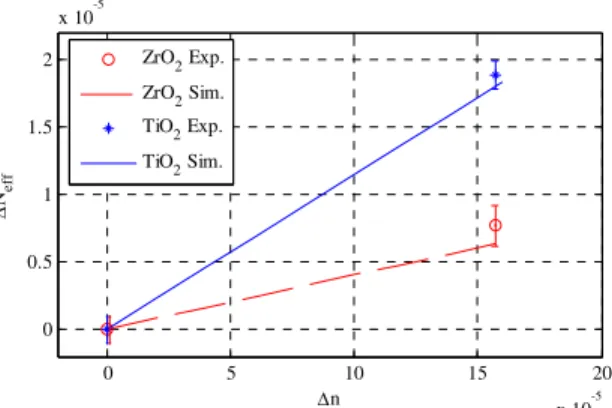
Knowing the phase shift φ, the effective index change Neff, and the corresponding
refractive index change n (Fig. 8), the slope of the sensitivity curve (S= Neff/ n) is
calculated, with results shown in Table 3. Note that the sensitivity S is defined with respect to the infiltrated gas refractive index change n, and is different from the modal sensitivity Sm
defined above with respect to the change of the average cladding index (porous film plus gas). Without the porous structure, S becomes equal to Sm and hence would be negligibly small for
gas refractive indices. The error bars around the experimental points take into account the error introduced by the curve fitting procedure and the noise associated with the measured signal; they correspond to one standard deviation of Neff calculated from data sets
representing three repeated measurements.
0 5 10 15 20 x 10-5 0 0.5 1 1.5 2 x 10⁻⁵ n Ne ff ZrO2 Exp. ZrO2 Sim. TiO2 Exp. TiO2 Sim.
Fig. 8. Sensitivity comparison for devices with ZrO2 and TiO2 film on the sensing layer.
For comparison, MZI simulated sensitivities obtained for structures similar to the one shown in Fig. 1, with an “effective” cladding layer refractive index 1.42 and 1.51 in the sensing window (corresponding to ZrO2 and TiO2 GLAD films), and the waveguide cross
0 to 16e-5 in ten steps produces linear responses, with higher slope obtained for device with TiO2 in the sensing window.
Both experimental and simulated results of Fig. 8 are in a good agreement; higher sensitivity has been achieved by the device with TiO2 film. As predicted by the modal
sensitivity curve of Fig. 2, a higher refractive index of sensing layer shifts the device operation point toward a higher slope region, thus providing better sensing abilities. Experimental results demonstrate that sensitivity is strongly affected by the core-cladding refractive index difference. Of course, this presents an important aspect of this optical sensing platform: any suitable arrangement of a dielectric structured thin film with a planar waveguide may result in an optical sensing device and, hence, adjustments on the sensing layer refractive index will enhance sensitivity of the device.
Table 3. The slope of the sensitivity curve for devices with ZrO2 and TiO2.
Device φ Neff S
ZrO2 π/16 7.6705e-6 0.0489
TiO2 π/10 1.8837e-5 0.1200
Time response of a MZI output can also be employed for refractive index determination. This measurement encounters the time response of porous cladding, and the gas system (the chemical formation inside the cell is changing gradually as a result of its cross sectional dimensions being different from those of the input gas pipe). Measurements were completed for TE polarized light at λ=1620 nm. As a result, devices will operate on the linear part of the transfer function, where any change in the refractive index value corresponds to a change in power output. Time response was measured for alternating N2 and CO2 gas flow on the
sensing environment. After filtering out the high frequency noise coupled with the signal, the measured time response of devices with ZrO2 and TiO2 is shown in Fig. 9.
0 500 1000 1500 2000 2500 -11.8 -11.6 -11.4 -11.2 -11 -10.8 -10.6 Time(sec) Po u t ( d B m ) N2 CO2 N2 CO2 N2 0 500 1000 1500 2000 2500 -11.8 -11.6 -11.4 -11.2 -11 -10.8 -10.6 Time(sec) Po u t ( d B m ) N2 CO2 N2 CO2 N2 (a) (b)
Fig. 9. Time response for alternating N2 and CO2 in the gas cell, device with (a) ZrO2, and (b)
TiO2 film.
While the output time response patterns of Fig. 9 look similar in both devices, there is a quantitative difference. When CO2 is introduced in the sensing environment, the output signal
of the device with ZrO2 film is increase by 0.38 dBm. In contrast, the output signal of the
device with TiO2 film decreases by 0.65 dBm. While the sine of Pout depends on the
wavelength of operation and has no significance for sensitivity evaluation, its absolute value is a clear indication that devices with TiO2 can achieve higher sensitivities. As demonstrated,
| Pout| for a device with TiO2 is almost twice that of a device with ZrO2, for the same n,
which is in complete agreement with results of Fig. 8.
Also, looking at the time response plots, a qualitative observation can be drawn. While the output power changes instantly when switching from N2 to CO2, there is a time constant when
but only 80 s to replace it with CO2. This could be due to a higher density, and/or a higher
sticking coefficient of CO2 as compared to N2. Note here that sticking coefficient is a
parameter used in surface physics to describe the ratio of the number of molecules that do absorb to a surface to the total number of atoms that impinge upon that surface during the same period of time. However, in order to fully understand this phenomenon, further investigations would be required. In general, a more porous film would result in faster exchange times, addressing the time constant issue, but at the expense of sensitivity because of the lowering of the effective NTF refractive index.
6. Conclusion
A new sensing platform for highly efficient optical sensing based on dielectric material NTF as sensing environment has been presented. By changing very few deposition parameters such as flux incidence angle or angular velocity of substrate rotation, a broad range of NTFs specific to individual applications can be created. Sensing ability of this new platform was demonstrated through design, fabrication, and characterization of interferometer-based devices with ZrO2 or TiO2 NTF as sensing environment. Sensitivity of fabricated devices was
experimentally confirmed with the refractive index measurement of a known gas. By alternating gas content in the sensing environment and measuring the frequency response, a maximum phase shift of φ=π/10 on the MZI transmission spectra was achieved. Devices with TiO2 film deposited on the sensing area performed much better than devices with ZrO2, with
sensitivity twice as high, demonstrating an important aspect of this optical sensing platform: any suitable arrangement of a dielectric structured thin film with a planar waveguide may result in an optical sensing device.
Acknowledgment
This work was supported by the Natural Sciences and Engineering Research Council of Canada (NSERC) and by the Canada Research Chairs program.