HAL Id: hal-01024749
https://hal.archives-ouvertes.fr/hal-01024749
Submitted on 16 Jul 2014
HAL is a multi-disciplinary open access
archive for the deposit and dissemination of
sci-entific research documents, whether they are
pub-lished or not. The documents may come from
teaching and research institutions in France or
abroad, or from public or private research centers.
L’archive ouverte pluridisciplinaire HAL, est
destinée au dépôt et à la diffusion de documents
scientifiques de niveau recherche, publiés ou non,
émanant des établissements d’enseignement et de
recherche français ou étrangers, des laboratoires
publics ou privés.
Photodiode nonlinear modeling and its impact on
optical links phase noise
Zeina Abdallah, Alexandre Rumeau, Arnaud Fernandez, Olivier Llopis,
Jérémy Maxin, Grégoire Pillet, Loïc Morvan, Gilles Cibiel
To cite this version:
Zeina Abdallah, Alexandre Rumeau, Arnaud Fernandez, Olivier Llopis, Jérémy Maxin, et al..
Photo-diode nonlinear modeling and its impact on optical links phase noise. European Frequency and Time
Forum ( EFTF ), Jun 2014, Neuchâtel, Switzerland. 6p. �hal-01024749�
Photodiode nonlinear modeling
and its impact on optical links phase noise
Z. Abdallah
1,4, A. Rumeau
1, A. Fernandez
1,2,
O. Llopis
11CNRS, LAAS, Univ. de Toulouse, Toulouse, France 2Univ. de Toulouse, UPS, Toulouse, France
J. Maxin
3, G. Pillet
3, L. Morvan
3, G. Cibiel
43Thales R&T, Palaiseau, France 4CNES, Toulouse, France
Abstract—The photodiode impact on the phase noise of an
optical link, and particularly its ability to convert the laser amplitude noise into microwave phase noise, is studied and modeled. The model involves a nonlinear RC cell which describes a photogeneration delay which is a function of the optical power. The whole system is then implemented on a microwave CAD software, and the link gain and phase noise performance are computed.
Keywords—photodiode; nonlinear modelling; CAD; microwave-optics; phase noise; optical fiber link
I. INTRODUCTION
Fiber optics links are widely used for time and frequency applications. These systems are able to transfer a clock or a frequency reference signal on a long distance. They may be used also for short distance frequency distribution, particularly in embedded systems (plane, satellite, boat) where they efficiently replace coaxial cables thanks to the low size, low mass and wide bandwidth of the optical fiber. Finally, fiber optics devices are the earth of some frequency generation systems, such as optoelectronic oscillators (OEO) [1] and optical comb frequency references [2].
In all these systems, the noise added to the microwave signal by the optical link is a problem, and the challenge is to reduce as much as possible its contribution. The noise floor and the carrier to noise ratio (CNR) of an optical link are well known and can be computed using textbook formulas [3] which involve some classical parameters such as the laser (high frequency) relative intensity noise (RIN), the photodiode shot noise and the load thermal noise. When a sinusoidal signal is transmitted through the optical link, the phase noise floor in rad2/Hz is the inverse of the link CNR. However, if
such an approach is able to describe the far from carrier phase noise floor of the optical link, it is unable to describe it’s close to carrier phase noise.
The close to carrier phase noise is the result of various nonlinear processes able to fold the devices low frequency (LF) noise components around the radio frequency (RF) carrier. The devices featuring LF noise in an optical link are mainly the laser and the optical fiber. The laser is affected by amplitude and frequency fluctuations, which both feature a 1/f like shape at low frequency (of course, the shape can vary
largely from pure 1/f spectrum to a spectrum with various and complex slopes, depending on the physical processes involved in the laser). The laser frequency noise (FM noise) can be demodulated in a system where the frequency dispersion is high, such as in an optical fiber of a few kilometers [4]. The laser amplitude noise (AM noise) will be more easily converted into phase noise by any component for which the transit time depends on the optical power, and this is the case of the photodiode [5]. The optical fiber may also generate a low frequency phase fluctuation, if it is long enough (a few kilometers) and if it is fed with a relatively high optical power [6]. This is due to phenomena such as Rayleigh scattering or Brillouin scattering. Fortunately, these phenomena can be controlled by limiting the optical power and, if possible, by using optical isolators.
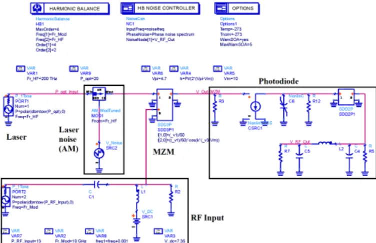
Figure 1 : Model of an optical link on ADS including an optical source with amplitude noise (AM modulator) and a Mach Zehnder modulator (MZM)
Compared to the laser, the excess low frequency noise of the photodiode is very weak. By proper cancelation of the laser AM noise with balanced photodiodes, this LF noise has been measured to be about 25 dB lower than the laser induced current fluctuations noise [6]. Therefore, the only noise source associated to the photodiode in our model is its shot noise.
However, the even if the photodiode is not a noisy device, it is able to convert the laser amplitude fluctuations into RF phase fluctuations. This phenomenon has been described by different authors and has been taken into account for the
optimization of OEOs [5,7]. It was therefore essential to include its description in our modeling approach of microwave optical links and systems.
This approach has been detailed elsewhere [8]. It is based on a commercially available harmonic balance microwave circuit design software (ADS), in which the optical elements have been described with the equivalent electrical circuit approach or with equivalent mathematical black box models (Figure 1). The laser is described using an amplitude modulated frequency source and the Mach Zehnder modulator is described with its 1+cos x response in a symbolically defined device (SDD). Up to now, this model was unable to compute the optical link 1/f phase noise. With the introduction of a nonlinear model of the photodiode, a 1/f phase noise component can now be observed.
II. PHOTODIODE MODELLING
In the above described model, the photodiode was up to now described by a quadratic detector, i.e. a current generator proportional to the optical power, followed by a passive circuit network in charge of the modeling of the photodiode frequency response. However, in real world, the photodetection is not instantaneous, and a delay has to be included in the model. This delay depends on the number of carrier generated, and increases with this number [9], and then decreases again when the photodiode saturates. This phenomenon directly translates into RF phase variations with an increase of the phase with the optical power at low optical power, and then a decrease. It is thus obvious that any amplitude fluctuation of the optical power will be converted into a fluctuation of the RF phase at the photodiode output.
Different photodiode models have been published [10-13], using different equivalent circuit approaches. However these models focus more on the amplitude response, or on the intermodulation response, than on the phase response. We have thus derived our own model, taking into account some of the approaches already proposed by the preceding authors, and particularly the description of the delay using an RC cell [11]. The model is depicted in Figure 2. It is composed of three successive cells: a nonlinear RC cell to describe the photogeneration delay, a black box which consists in an isolator with a current compression equation (to describe the amplitude saturation) and the output filtering network (to take into account the limited frequency bandwidth). In the RC cell, only the capacitance is nonlinear, and it is described with a second order polynomial expression. The current compression cell involves an hyperbolic tangent function to make the current saturate at a given value.
To compute the model parameters, it is necessary to measure the photodiode RF phase response. This is performed with the measurement bench described in Figure 3, using a vector network analyser (VNA). The optical power on the photodiode is controlled in this set up thanks to an optical attenuator located just before the device under study, in order to keep all the other devices (laser, MZM) in the same operating conditions. The MZM is stabilized either using a passive temperature control or an active bias control system.
Figure 2 : Details of the photodiode nonlinear model : 1) quadratic detection and photocurrent generation ; 2) transit time RC cell ; 3) current saturation description with a SDD ; 4) output filtering network (parasitic capacitances, inductances…) laser
Att
VNA
EDFA MZM RFin RFout 1 2Figure 3 : Set-up for the measurement of the RF phase sensitivity to the optical power received by the photodiode. The MZM is maintained at quadrature and only the optical attenuator is changed during the measurement.
Figure 4 : RF phase measurement at three different frequencies : 2 GHz, 5 GHz and 10 GHz. The measured data are compared to the simulated data obtained using the equivalent model of Figure 2.
The measurement of the phase of the S21 parameter is
depicted in Figure 3 for a Discovery DSC30S photodiode. It shows the characteristic shape already observed in the past [5,7], with a maximum at which the conversion of optical AM to RF phase is null. In the case of the measured photodiode, this maximum is close to 10 mW optical power. Also the phase change with the optical power increases with the increase of RF frequency, as shown in the figure for three frequencies : 2 GHz, 5 GHz and 10 GHz.
The parameters of the model depicted in Figure 2 are then adjusted to fit the measured data. A fit is possible with a nonlinear capacitance described by an order two polynomial expression (versus the voltage seen by the capacitance). The three coefficients of the polynomial expression are thus adjusted to fit the phase measurements simultaneously at the three measured frequencies, and the results are depicted in figure 4. In spite of the model simplicity, the variation of the RF phase is efficiently described: the simulated phase maximum is close to 10 mW, the general shape of the curve is very similar to the measured one and the increase of the phase with the RF frequency is well described. Of course, better precision could be obtained with a more complex model, but taking into account the difficulty of such phase variations measurements (less than 2° overall variation), which requires a difficult calibration procedure and a good thermal control of the devices (particularly the Mach Zehnder modulator), the proposed model appears to be well fitted to the applications. The final error in phase is less than 0.3°, which is close to the measurement precision. Moreover, a simple model (same set of parameters whatever the RF frequency) is much safer with respect to further computations, and particularly for the convergence of the harmonic balance software.
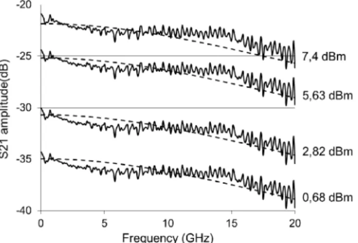
Figure 5 : S21 amplitude variations with the RF frequency and the received optical power. Measurement (solid line) and model (dashed line).
The amplitude variations of the S21 parameter are also
described in the model, as shown in Figure 5. In this figure, the frequency response of the photodiode is depicted at different optical power levels. The amount of optical power received does not change this frequency response, but the RF output power increases with this optical power with a 2 dB RF gain every 1 dB optical power gain, up to the photodiode saturation power.
III. PHASE NOISE SIMULATION
The harmonic balance technique involved in ADS is a simulation approach which is able to compute the performance of a circuit or a system operating at different frequencies, with a large gap between each frequency. This is due to a description in the frequency domain instead of the time domain. Only the nonlinearities are computed in the time domain and the result is fed-back to the simulator through a fast Fourier transform. In our simulations of optical microwave systems, three different spectral domain are concerned: the low frequency range (DC to 100 kHz), the RF range (ex: a 10 GHz signal and its harmonics) and the optical range (194 THz). The harmonic balance approach is perfectly fitted to this problem since it only takes into account the frequencies that have been selected to be the simulation frequencies.
Concerning the noise simulation, the harmonic balance approach includes a specific module which is able to compute the effect of a small perturbation at a given frequency on any other simulation frequencies, in amplitude and phase. This module not only allows the description of a quasi static perturbation, but is also able to take into account a possible frequency dispersion in a small frequency bandwidth around any of the simulation frequencies. In other words, it is the perfect tool to compute the conversion of a noise at a given frequency towards another frequency of the analysis (in this case, the RF frequency).
In the model depicted in Figure 1, the only noisy device is the laser. It is described by its amplitude noise (RIN), thanks to an amplitude modulator. The phase noise of the laser could also be easily included in the model. However, in this case, there is no element in the model able to perform a conversion of such noise. In a near future, a model of a dispersive optical fiber will be included in this approach, and in this case the laser frequency noise will be of interest. Finally, for the noise simulations, a shot noise source is added to the photodiode model (current white noise of spectral density 2qIo , with q
being the electron charge and Io the DC photocurrent).
Figure 6 : RIN simulated with ADS at the photodiode output around DC frequency (fitted to the laser measured data).
The parameters of the noise source feeding the AM modulator are then adjusted such that the laser RIN simulated
around DC on the photodiode can fit the measured LF RIN of the laser. This noise source is simply described by the sum of a 1/f noise and a noise floor. Figure 6 depicts the simulated RIN for three optical power levels. These results corresponds to measurements spectra which have been obtained on a high power EM4 semiconductor DFB laser, similar to the measurements described in ref [4] for the same device.
A first solution to compute the effect on the phase noise of a single noise source is to compute the transfer coefficient between this noise source and the RF phase noise. This coefficient corresponds to the slope of the Figure 4 curve, and is depicted in Figure 7. However, this approach may lead to errors if other noise sources have to be considered.
Figure 7 : Conversion coefficient between RF phase and optical power
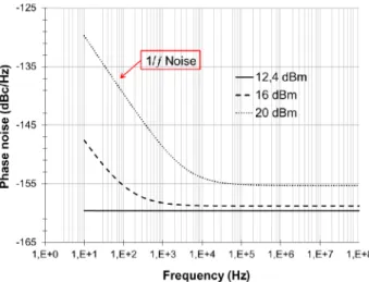
Figure 8 : Simulated phase noise around the RF carrier (10 GHz) at different optical power levels.
The 10 GHz phase noise is thus more efficiently computed with ADS using the dedicated variable for nonlinear noise simulation (pnmx). The result is depicted in Figure 8. As shown in this figure, the only important 1/f noise contribution which appears in the simulated data is at high optical power level (20 dBm). Further work has to be performed to compare these data to the measurement. However, such a comparison is difficult because the optical amplifier used in this experiment is also noisy [14] and it is hard to discriminate between the laser noise and the amplifier noise.
IV. CONCLUSION
A model of a microwave photodiode, able to describe the nonlinear transit time effects, has been presented. This model is relatively simple and compares well with the simulated data, and particularly the microwave phase data at various microwave frequencies. It has been included in a model describing a complete optical link and has been used to simulate the residual phase noise of this link. The model predicts the conversion of the laser amplitude noise into microwave phase noise, and could be use efficiently to evaluate not only the noise of the optical link but also optoelectronic oscillators phase noise.
ACKNOWLEDGMENTS
This work is supported by CNES, the Regional Council of Midi Pyrénées, and the French MOD through DGA-ANR-11-ASTR-0029 MINOTOR contract.
REFERENCES
[1] X. S. Yao and L. Maleki, ″Optoelectronic microwave oscillator″, J. Opt. Soc. Am. B, Vol. 13, No. 8, August 1996, pp. 1725-1735.
[2] T. M. Fortier et al., “Generation of ultrastable microwaves via optical frequency division”, Nature Photonics, June 2011, pp. 425-429. [3] G.P. Agrawal, « Fiber-Optic Communication Systems » Wiley, 1997. [4] H. Brahimi, P. Lacroix, O. Llopis, “Optimisation of a microwave
frequency discriminator based on an optical delay line”, IEEE Int. Topical Meeting on Microwave Photonics (MWP), Valencia, Oct. 2009. [5] D. Eliyahu, D. Seidel, L. Maleki, ″RF Amplitude and Phase-Noise
Reduction of an Optical Link and an Opto-Electronic Oscillator″, IEEE Trans. on MTT, vol. 56, no 2, Feb. 2008, pp. 449-456.
[6] O. Llopis, S. Azaizia, K. Saleh, A. Ali Slimane, A. Fernandez, “Photodiode 1/f noise and other types of less known baseband noises in optical telecommunications devices”, Proc. of the Int. Conf. on Noise and Fluctuations (ICNF 2013), Montpellier, June 2013.
[7] K. Saleh, O. Llopis, G. Cibiel, “Optical Scattering Induced Noise in Fiber Ring Resonators and Optoelectronic Oscillators”, Journal of Lightwave Technology, vol. 31, no. 9, pp. 1433,1446, May 1, 2013. [8] H. Brahimi, H.L. Martinez-Reyes, P.H. Merrer, A. Bouchier, O. Llopis,
″A CAD approach of Microwave Optical Systems including Noise performance″, Proc. of the 2009 European Microwave Conf. (EuMC), Rome, Italy, 2009, pp. 1642-1645.
[9] W. Zhang, T. Li, M. Lours, S. Seidelin, G. Santarelli, and Y. Le Coq, ″Amplitude to phase conversion of InGaAs pin photo-diodes for femtosecond lasers microwave signal generation″, Appl. Phys. B, vol 106, issue 2, Feb. 2012, pp. 301-308.
[10] G. Wang, T. Tokumitsu, I. Hanawa, Y. Yoneda, K. Sato, M. Kobayashi, ″A time-Delay Equivalent-Circuit Model of Ultrafast p-i-n Photodiodes″, IEEE Trans. on Microwave Theory and Techniques, vol. 51, no. 4, April 2003, pp. 1227-1233.
[11] M. Piels, A. Ramaswamy, and J. E. Bowers, ″Nonlinear modeling of waveguide photodetectors,″ Optics Express, vol. 21, no. 13, pp. 15634-15644, 2013.
[12] H. Jiang and P. K. L. Yu, ″Equivalent Circuit Analysis of Harmonic Distortions in Photodiode″, IEEE Photonics Technology Letters, vol. 10, no 11, November 1998, pp. 1608-1610.
[13] M. Nikoufard, X.J.M. Leijtens, Y.C. Zhu, T.J.J. Kwaspen, E.A.J.M Bente, F.H. Groen, and M.K. Smit, ″Modelling and Characterization of InP-Based high-speed pin-photodiode″, Proceedings Symposium IEEE/LEOS Benelux Chapter, 2003, Enschede.
[14] V. Auroux, A. Fernandez, O. Llopis, P.H. Merrer, A. Vouzellaud, ″Microwave phase noise properties of optical links involving small signal and gain saturated optical amplifiers″, this conference (EFTF 2014).