HAL Id: hal-02088294
https://hal.archives-ouvertes.fr/hal-02088294
Submitted on 23 Apr 2019HAL is a multi-disciplinary open access archive for the deposit and dissemination of sci-entific research documents, whether they are pub-lished or not. The documents may come from teaching and research institutions in France or abroad, or from public or private research centers.
L’archive ouverte pluridisciplinaire HAL, est destinée au dépôt et à la diffusion de documents scientifiques de niveau recherche, publiés ou non, émanant des établissements d’enseignement et de recherche français ou étrangers, des laboratoires publics ou privés.
Thermionic-enhanced near-field thermophotovoltaics for
medium-grade heat sources
A. Datas, R. Vaillon
To cite this version:
A. Datas, R. Vaillon. Thermionic-enhanced near-field thermophotovoltaics for medium-grade heat sources. Applied Physics Letters, American Institute of Physics, 2019, 114 (13), pp.133501. �10.1063/1.5078602�. �hal-02088294�
Thermionic-enhanced near-field thermophotovoltaics
1
for medium-grade heat sources
2
A. Datas1,2* and R. Vaillon3,1,4
3
1Instituto de Energía Solar, Universidad Politécnica de Madrid, 28040 Madrid, Spain
4
2Universitat Politécnica de Catalunya, Jordi Girona 1-3, Barcelona 08034, Spain
5
3Univ Lyon, CNRS, INSA-Lyon, Université Claude Bernard Lyon 1, CETHIL
6
UMR5008, F-69621, Villeurbanne, France
7
4IES, Univ. Montpellier, CNRS, F-34000 Montpellier, France
8
* Corresponding author: Alejandro Datas (a.datas@ies.upm.es) 9
Keywords: thermophotovoltaics, thermionics, near-field radiation, waste heat recovery.
10 11
Abstract
12
Conversion of medium-grade heat (temperature from 500 to 1000 K) into electricity is 13
important in applications such as waste heat recovery, or power generation in solar thermal and 14
co-generation systems. At such temperatures, current solid-state devices lack of either high 15
conversion efficiency (thermoelectrics) or high-power density capacity (thermophotovoltaics 16
and thermionics). Near-field thermophotovoltaics (nTPV) theoretically enables high power 17
density and conversion efficiency by exploiting the enhancement of thermal radiation between a 18
hot emitter and a photovoltaic cell separated by nanometric vacuum gaps. However, significant 19
improvements are possible only at very small gap distances (< 100 nm), and when ohmic losses 20
in the photovoltaic cell are negligible. Both requirements are very challenging for current device 21
designs. In this work, we present a thermionic-enhanced near-field thermophotovoltaic (nTiPV) 22
converter consisting of a thermionic emitter (graphite) and a narrow bandgap photovoltaic cell 23
(InAs) coated with low-workfunction nanodiamond films. Thermionic emission through the 24
vacuum gap electrically interconnects the emitter with the front side of the photovoltaic cell and 25
generates an additional thermionic voltage. This avoids the use of metal grids at the front of the 26
cell, and virtually eliminates the ohmic losses, which are unavoidable in realistic nTPV devices. 27
We show that nTiPV operating at 1000 K and with a realizable vacuum gap distance of 100 nm, 28
enables a 10.7-fold enhancement in electrical power (6.73 W/cm2) and a 2.8-fold enhancement
29
in conversion efficiency (18 %) in comparison with a realistic nTPV device having a series 30
resistance of 10 mΩ·cm2.
31
1. Introduction
32
Thermionics (TIC) 1,2 and thermophotovoltaics (TPV) 3,4 are highly efficient alternatives to
33
thermoelectric generators (TEG) 5. In TIC, electrons are thermally emitted from a hot
34
emitter/cathode and collected in a cold anode/collector, subsequently producing an electrical 35
current. In TPV, thermally radiated photons are absorbed in a low-bandgap semiconductor and 36
excite electron-hole pairs, which are selectively collected to produce an electrical current. Both 37
TPV and TIC have already demonstrated higher conversion efficiencies than TEG at 38
temperatures beyond 1000 ºC (~ 24 % for TPV 6,7 and ~ 11% for TIC 1). However, the power
39
density is comparatively very low (e.g. less than 1 W/cm2 for TPV at 1039 ºC 6, while ~ 20
40
W/cm2 for TEG at 595 ºC 8). The main reason is the lower energy flux of radiated particles
41
compared with that carried by the electrons moved by a temperature gradient within a solid, as 42
in TEG. 43
Boosting the power density of TIC and TPV is the motivation of current research efforts that 44
aim at increasing the flux of radiated photons (for TPV) and electrons (for TIC). For TIC, most 45
of the research focuses on reducing the workfunction of the emitter and collector, along with 46
reducing the accumulated space-charge by applying magnetic fields or by reducing the vacuum 47
gap that separates the cathode and the anode to micrometric scales 1,2. For TPV, at least three
48
strategies were proposed for increasing the energy flux of radiated photons at moderate 49
temperatures: light-pipe TPV (LTPV) 9, thermophotonics (TPX) 10, and near-field
50
thermophotovoltaics (nTPV) 11. Recently, a combination of the last two has been also proposed
51
12. nTPV is the strategy with the highest theoretical potential. It consists of creating nanoscale
52
vacuum gaps between the emitter and the photovoltaic (PV) cell, so that evanescent waves 53
(photons) tunnel from the emitter to the cell and contribute to generating electrical power. Near-54
field thermal radiation transport was thoroughly investigated from both theoretical and 55
experimental points of view 13,14, and its potential use for heat-to-electricity conversion widely
56
analyzed 15. Only very recently the proof-of concept of nTPV has been finally achieved by
57
measuring a 40-fold enhancement of the electrical output power at gap distances of less than 58
100 nm 16. However, nTPV has (at least) two main relevant issues that may impede its further
59
deployment: first, the quite high ohmic losses due to the very high current densities that must 60
flow laterally through thin semiconductor layers within the PV cell; second, the very small 61
vacuum gaps that are needed to obtain a significant improvement in electrical power density. 62
In this work, we present a theoretical analysis of a thermionic-enhanced nTPV device (nTiPV) 63
that eliminates the ohmic losses and enables higher power densities at larger gap distances than 64
conventional nTPV. It is the aim of this work to illustrate the theoretical potential of a specific 65
device with a medium-grade heat source operating at a temperature of 1000 K. 66
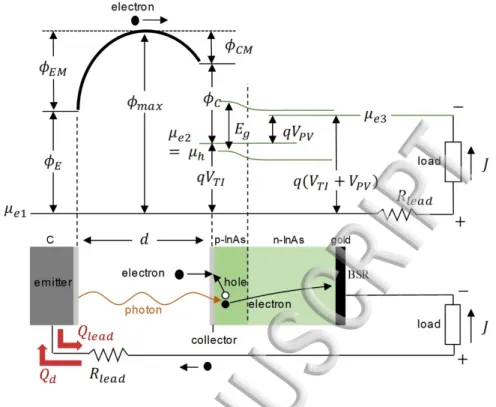
2. Device concept
67
Figure 1 shows the band diagram of the proposed device, which is the near-field counterpart of
68
the hybrid thermionic-photovoltaic concept introduced previously 17. The system consists of a
69
graphite emitter and an InAs (bandgap of 0.35 eV at 300 K) PV cell separated by a distance d. 70
The emitter and the PV cell are coated with very thin (~ 1-2 nm) transparent H-terminated 71
diamond films, which have been proved experimentally to provide workfunctions in the range 72
of around 1.4 eV (N-doped films 18) down to around 0.9 eV (P-doped films 19). The emitter is
73
heated by an external heat source, and subsequently radiates photons and electrons towards the 74
PV cell. Due to the emission of electrons, the emitter surface is charged positively. Thus, the 75
radiated electrons are attracted back, and if the distance d is relatively large, they accumulate in 76
the vacuum gap. This regime of operation is named “space-charge-limited” mode, and it is 77
characterized by additional potential barriers ɸEM and ɸCM that oppose to the electrons’ flow. On
78
the contrary, if the distance d is small, the radiated electrons are effectively collected at the InAs 79
PV cell surface, without accumulating in the gap, subsequently eliminating any kind of potential 80
barrier, and leading to a drastic enhancement of the thermionic current. When the thermionically 81
emitted electrons reach the PV cell surface, they recombine with the holes photogenerated in the 82
PV cell. Ideally, no electrical potential is created in this process, as in ideal ohmic contacts. 83
Therefore, the full PV cell front side behaves as a transparent collector that ensures the wireless 84
electrical connection between the emitter and the PV cell. The output voltage is thus the 85
addition of the thermionic voltage ( , generated between the emitter and the front side of the 86
PV cell) and the photovoltaic voltage ( , generated between the front and rear sides of the PV 87
cell). Remarkably, this design avoids the use of front metal grids, eliminating the subsequent 88
shadowing losses, and mitigating the challenges of nano-gap implementation in space-89
constrained near-field TPV devices. In conventional PV cells, either in front- or back-contacted 90
configurations, the main contributors to the ohmic losses are the currents that flow laterally 91
through the semiconductor and metal layers. These losses are fully eliminated in the nTiPV 92
device, where the current flow is nearly unidirectional and transversal to the device’s area. 93
Results will show that this is a particularly significant benefit for near-field operation, which 94
involves very large current densities. 95
The far-field counterpart of this device 17 is being experimentally developed 20,21. The
96
experimental device operates in ultra-high vacuum (UHV) conditions and uses dielectric micro-97
spacers to create a micrometer vacuum gap between the emitter and the PV cell. Modern 98
microfabrication techniques already enabled the development of thermally and electrically 99
insulated spacers that withstand large temperature gradients. These techniques eventually 100
enabled the experimental demonstration of micron-gap TIC 22,23. Sub-micron separation
101
distances were also experimentally realized using nano-spacers in the frame of near-field 102
thermal radiation experiments 24–27. Despite the recent experimental demonstration of nTPV 16
103
was realized using a suspended emitter and precise alignment tools, current research efforts 104
target the integration of spacers into stable nano-gap nTPV devices 28. All these recent
105
progresses should be directly transferrable to the experimental implementation of nTiPV 106
devices. 107
3. Methods
108
Analysis of the nTiPV device described above requires the calculation of the total net flux of 109
photons and electrons through nanoscale vacuum gaps, along with the generated current-voltage 110
characteristics for both thermionic and photovoltaic converters in the near field. 111
For the thermionic part, the electrons’ energy flux ( ), the generated current density ( ) and 112
output voltage ( ), can be calculated by neglecting collector’s back emission as 29
113
2 114
115
116
where A is the Richardson-Dushman constant, k is the Boltzman constant, q is the electron’s 117
charge, and is the emitter temperature. is the maximum of the electric potential created 118
along the inter-electrode gap (Figure 1). In the space-charge-limited mode, 119
or , ( ) being the emitter’s (collector’s) workfunction. The 120
values of energy barriers and can be calculated using the Langmuir theory 29. This
121
theory assumes one-dimensional and collision-less electron flow with a half-Maxwellian 122
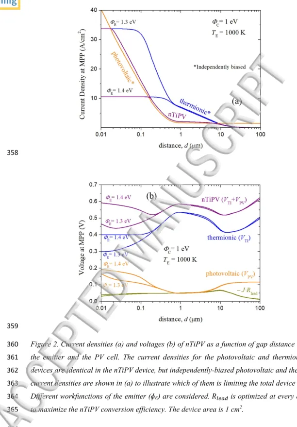
distribution of velocities. In the so-called retarding mode, is large enough to locate the 123
maximum of the electrostatic potential at the collector’s surface, i.e. . The 124
latter will be the most typical case in the near field, where the very small inter-electrode 125
distance will nearly eliminate the barriers and and the maximum power point (MPP) 126
will happen at and . In order to analyze the theoretical potential of 127
the concept, a Richardson constant of 120 A/cm2 is assumed. Significant deviations from this
128
theoretical value are possible depending on the experimental conditions of the deposition of the 129
emitter film, as well as on the interfacial layers that could be created during this process 18.
130
For the photovoltaic part, the photons’ energy flux is calculated using fluctuational 131
electrodynamics 30 and the S-matrix method for 1D-layered media 31. The current density ( ) –
132
voltage ( ) characteristic is calculated by solving the minority carrier diffusion equation in 133
the frame of the low-injection approximation, using methods described elsewhere 32,33. The
134
device consists of four layers sandwiched between two semi-infinite media, respectively made 135
of graphite (emitter, semi-infinite), vacuum (gap with variable thickness d), p-doped InAs (Na =
136
1018 cm-3, 0.75 m thick), n-doped InAs (N
d = 1016 cm-3, 6 m thick), gold (back surface
137
reflector, 200 nm thick) and vacuum (semi-infinite). Radiative, Auger, and Shockley–Read– 138
Hall (SRH) recombination mechanisms are considered with parameters from 34, along with
139
finite doping and temperature-dependent mobilities for electrons and holes 35. The model
140
assumes that the thermionic layer on the PV cell does not modify the PV cell band diagram in a 141
way that holes could not diffuse towards the thermionic collector. This is a reasonable 142
assumption given the presence of electrically active defects in the semiconductor-diamond 143
interface, as well as the very high doping levels of both the p-doped InAs layer and the diamond 144
thin film, both effects preventing the creation of Schottky barriers in the semiconductor-145
diamond interface 18,36,37. Optical properties of InAs corresponding to interband absorption and
146
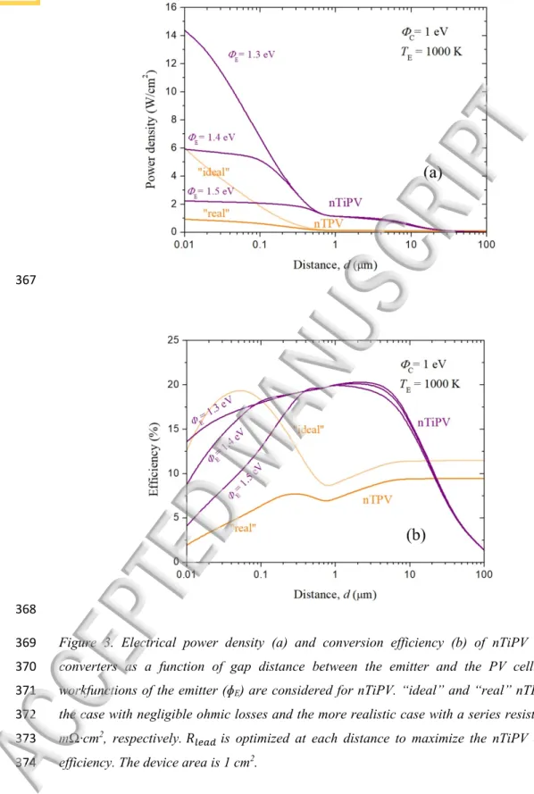
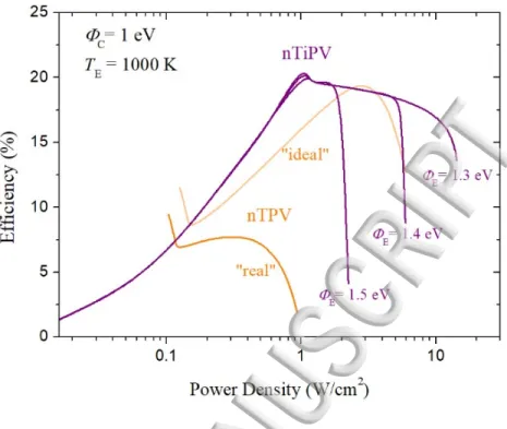
interactions with free carriers and phonons, are calculated using the method described in 38 and
147
the Drude-Lorentz model 39, respectively, with the parameters of 40. The Drude model is used
148
for gold 41. For the sake of simplicity, diamond layers are omitted in the radiation transfer
149
calculations. Their impact on emission by the graphite emitter and absorption by the InAs cell is 150
assumed to be negligible, because layers are every thin (~1-2 nm), diamond’s extinction 151
coefficient is weak, and diamond’s refractive index is of intermediate level between that of 152
graphite and indium arsenide 42.
153
Finally, the nTiPV conversion efficiency is given by 154
max
155
where max is the maximum electrical power at a current density 156
and voltage . ⁄2 is the minimum 157
amount of heat lost through the emitter’s leads having an electrical resistance , is 158
the Lorentz number of the metal 29, and ⁄ represents the heat generated in the 2
159
leads by Joule effect that is turned back to the emitter, being the device area, equal to 1 cm2 in
160
the current study. The value of can be optimized to fulfil a trade-off between heat losses 161
and power generation that ultimately maximizes conversion efficiency. For comparison 162
purposes, the conversion efficiency of a standalone nTPV device is calculated by 163
max⁄ , being the PV cell series resistance in Ω·cm2. In every
164
calculation involving the search for maximum values, the Nelder-Mead algorithm is used 43.
165
4. Results and Discussion
167
Figure 2 (a) (Figure 2 (b)) shows the generated current density (voltage) of the nTiPV device as
168
a function of gap distance d. Results are shown for two values of the emitter workfunction 169
( 1.3 and 1.4 eV), a fixed collector’s workfunction ( 1 eV), and an emitter temperature 170
of 1000 K. The lead resistance ( ) is optimized at every distance to maximize the 171
nTiPV conversion efficiency. The voltage generated in the photovoltaic ( ) and thermionic 172
( ) stages is also shown in Figure 2 (b), along with the voltage drop in the leads ( ). 173
As explained in the previous sections, both thermionic and photovoltaic currents must be 174
identical within the nTiPV device due to the series interconnection, i.e. . This 175
means that their respective internal voltages, and (see Figure 2 (b)), must be adapted to 176
meet this condition. However, the maximum power density attainable for each sub-device 177
would be higher if they were biased independently. This is illustrated in Figure 2 (a), which also 178
shows the current densities at the MPP for the independently-biased thermionic ( ∗ ) and
179
photovoltaic ( ∗ ) devices. This information is valuable for the following discussion. 180
There are three main different regions in Figure 2 (a). For large distances, thermionic emission 181
is strongly reduced by the space-charge effect, also illustrated by the larger thermionic voltage 182
contribution in Figure 2 (b), and limits the total current of the nTiPV device. This causes the PV 183
cell to be biased near open circuit. For intermediate distances, the space charge is mitigated and 184
the flux of thermionically emitted electrons exceeds that of photogenerated charges in the PV 185
cell. This causes an increase (decrease) of the thermionic (photovoltaic) voltage that reduces 186
(increases) the thermionic (photovoltaic) current until both thermionic and photovoltaic currents 187
are identical. In this region, the thermionic device undergoes the transition from space-charge-188
limited to saturation mode, and the photovoltaic device undergoes the transition from far field to 189
near field. The third region corresponds to the smallest distances at which photovoltaic 190
photogeneration exceeds the thermionic electrons’ flux due to the strong near-field enhancement 191
of photons’ flux. In this region, the thermionic current is already saturated, with no space-charge 192
effect, and limits the total current of the nTiPV device. Saturation of the thermionic sub-device 193
is characterized by voltages approaching at very small distances (0.3 and 0.4 eV 194
in Figure 2 (b)). The transitions through these three regimes take place at two specific distances 195
for which both thermionic and photovoltaic currents are equal. There is one in the near field and 196
another in the far field. Only at these specific distances, both thermionic and photovoltaic sub-197
devices are biased simultaneously at their respective MPP. In all other situations, one of the 198
devices produces a lower current and it is consequently biased at larger voltages than that of its 199
MPP. 200
Figure 3 shows the maximum electrical power density (Figure 3 (a)) and conversion efficiency
201
(Figure 3 (b)) of nTiPV as a function of gap distance. Figure 4 rearranges the results from these 202
figures to show conversion efficiency as a function of electrical power density. Results for two 203
kinds of “conventional” nTPV devices are also included: “ideal” nTPV assumes negligible 204
ohmic losses, and “real” nTPV assumes a PV cell with a series resistance of 10 mΩ·cm2.
205
nTiPV generally outperforms nTPV, especially when considering a “real” nTPV device with 206
non-negligible ohmic losses. Even in the case of an “ideal” nTPV (with negligible ohmic losses) 207
nTiPV outperforms nTPV provided that the inter-electrode distance is larger than 100 nm and 208
the emitter workfunction is lower than 1.5 eV. Impact of the emitter workfunction is evident for 209
small distances, where a low emitter workfunction (e.g. 1.3 eV) is needed to produce a 210
high enough thermionic current and fully exploit the enhancement of the photovoltaic power 211
generation in the near field. In the case of larger emitter workfunctions, the low thermionic 212
current limits the total current of the device and near-field effects are not fully exploited. At 213
larger distances, impact of the emitter’s workfunction is negligible because the nTiPV device is 214
limited either by the photovoltaic current or by the space charge. Quite importantly, nTiPV 215
produces a significantly higher power at larger (more feasible) gap distances (Figure 3 (a)). For 216
instance, a nTiPV device with an emitter (PV cell) surface workfunction of 1.3 eV (1 eV) 217
produces 6.73 W/cm2 for a gap distance of 100 nm. This is 3.7 times more electrical power than
218
an idealized nTPV device with negligible ohmic losses (1.82 W/cm2), and 10.7 times more
219
electrical power than a realistic nTPV device having a series resistance of 10 mΩ·cm2 (0.63
220
W/cm2). Besides, the conversion efficiency is similar to that of an idealized nTPV device (~ 18
221
%), but significantly higher than that of a realistic nTPV device with non-negligible ohmic 222
losses (6.4 %). Generally speaking, we can state that nTiPV operating at 1000 K theoretically 223
enables reaching power densities and conversion efficiencies greater than 10 W/cm2 and 15 %,
224
respectively, while realistic nTPV is limited to ~ 1 W/cm2 and ~ 7 % (Figure 4).
225
5. Conclusions
226
We have established a conceptual thermionic-enhanced near-field thermophotovoltaic (nTiPV) 227
device for the conversion of medium-grade heat into electricity. The converter comprises an 228
InAs photovoltaic cell and a graphite emitter separated by a nanometric vacuum gap, both 229
elements having engineered low workfunctions. Based on an analytical theoretical model that 230
combines fluctuational electrodynamics and the Langmuir theory, we have shown that nTiPV 231
produces significantly higher electrical power (6.73 W/cm2) and conversion efficiency (18 %)
232
than conventional near-field thermophotovoltaics (nTPV) using moderately large gap distances 233
(100 nm). The major advantages are the elimination of the ohmic losses and the enhancement of 234
the output voltage. According to these results, nTiPV could significantly outperform current 235
thermoelectric devices for the conversion of medium-grade heat sources into electricity. 236
6. Acknowledgements
237
This work has been partially funded by the project AMADEUS, which has received funds from 238
the European Union Horizon 2020 research and innovation program, FET-OPEN action, under 239
grant agreement 737054. The sole responsibility for the content of this publication lies with the 240
authors. It does not necessarily reflect the opinion of the European Union. Neither the REA nor 241
the European Commission are responsible for any use that may be made of the information 242
contained therein. A. Datas acknowledges postdoctoral fellowship support from the Spanish 243
"Juan de la Cierva-Incorporación" program (IJCI-2015-23747). R. Vaillon is thankful to the 244
Instituto de Energía Solar at the Universidad Politécnica de Madrid for hosting him, and 245
acknowledges the partial funding from the French National Research Agency (ANR) under 246
grant ANR-16-CE05-0013. Authors acknowledge Daniele Trucchi and Alessandro Bellucci for 247
the suggestion of using nanodiamond films as transparent low-workfunction coatings for the 248
emitter and the PV cell. 249 250 251 252 253 254 255 256 257 258 259 260 261 262
References
263
1 D.B. Go, J.R. Haase, J. George, J. Mannhart, R. Wanke, A. Nojeh, and R. Nemanich, Front.
264
Mech. Eng. 3, (2017). 265
2 K.A.A. Khalid, T.J. Leong, and K. Mohamed, IEEE Transactions on Electron Devices 63,
266
2231 (2016). 267
3 T. Bauer, Thermophotovoltaics: Basic Principles and Critical Aspects of System Design
268
(Springer, 2011). 269
4 D.L. Chubb, Fundamentals of Thermophotovoltaic Energy Conversion (Elsevier, 2007).
270
5 J. He and T.M. Tritt, Science 357, (2017).
271
6 B. Wernsman, R.R. Siergiej, S.D. Link, R.G. Mahorter, M.N. Palmisiano, R.J. Wehrer, R.W.
272
Schultz, G.P. Schmuck, R.L. Messham, S. Murray, C.S. Murray, F. Newman, D. Taylor, D.M. 273
DePoy, and T. Rahmlow, IEEE Transactions on Electron Devices 51, 512 (2004). 274
7 D.N. Woolf, E.A. Kadlec, D. Bethke, A.D. Grine, J.J. Nogan, J.G. Cederberg, D.B. Burckel,
275
T.S. Luk, E.A. Shaner, and J.M. Hensley, Optica, OPTICA 5, 213 (2018). 276
8 R. He, D. Kraemer, J. Mao, L. Zeng, Q. Jie, Y. Lan, C. Li, J. Shuai, H.S. Kim, Y. Liu, D.
277
Broido, C.-W. Chu, G. Chen, and Z. Ren, PNAS 113, 13576 (2016). 278
9 D.L. Chubb, AIP Conference Proceedings 890, 297 (2007).
279
10 N.-P. Harder and M.A. Green, Semicond. Sci. Technol. 18, S270 (2003).
280
11 J.L. Pan, H.K.H. Choy, and C.G. Fonstad, IEEE Transactions on Electron Devices 47, 241
281
(2000). 282
12 B. Zhao, P. Santhanam, K. Chen, S. Buddhiraju, and S. Fan, Nano Lett. 18, 5224 (2018).
283
13 B. Song, A. Fiorino, E. Meyhofer, and P. Reddy, AIP Advances 5, 053503 (2015).
284
14 J.C. Cuevas and F.J. García-Vidal, ACS Photonics 5, 3896 (2018).
285
15 E. Tervo, E. Bagherisereshki, and Z. Zhang, Front. Energy 12, 5 (2018).
286
16 A. Fiorino, L. Zhu, D. Thompson, R. Mittapally, P. Reddy, and E. Meyhofer, Nature
287
Nanotechnology 1 (2018). 288
17 A. Datas, Applied Physics Letters 108, 143503 (2016).
289
18 F.A.M. Koeck and R.J. Nemanich, Journal of Applied Physics 112, 113707 (2012).
290
19 F.A.M. Koeck, R.J. Nemanich, A. Lazea, and K. Haenen, Diamond and Related Materials 18,
291
789 (2009). 292
20 A. Datas, A.B. Cristobal, C. del Cañizo, E. Antolín, M. Beaughon, N. Nikolopoulos, A.
293
Nikolopoulos, M. Zeneli, N. Sobczak, W. Polkowski, M. Tangstad, J. Safarian, D.M. Trucchi, 294
A. Bellucci, M. Girolami, R. Marx, D. Bestenlehner, S. Lang, A. Vitulano, G. Sabbatella, and 295
A. Martí, in AIP Conference Proceedings (2018), p. 170004. 296
21 A. Mezzi, P. Soltani, S. Kaciulis, A. Bellucci, M. Girolami, M. Mastellone, and D.M.
297
Trucchi, Surface and Interface Analysis 50, (2018). 298
22 J.H. Lee, I. Bargatin, B.K. Vancil, T.O. Gwinn, R. Maboudian, N.A. Melosh, and R.T. Howe,
299
Journal of Microelectromechanical Systems 23, 1182 (2014). 300
23 R.Y. Belbachir, Z. An, and T. Ono, J. Micromech. Microeng. 24, 085009 (2014).
301
24 K. Ito, K. Nishikawa, A. Miura, H. Toshiyoshi, and H. Iizuka, Nano Lett. 17, 4347 (2017).
302
25 J.I. Watjen, B. Zhao, and Z.M. Zhang, Appl. Phys. Lett. 109, 203112 (2016).
303
26 M. Ghashami, H. Geng, T. Kim, N. Iacopino, S.K. Cho, and K. Park, Phys. Rev. Lett. 120,
304
175901 (2018). 305
27 K. Ito, A. Miura, H. Iizuka, and H. Toshiyoshi, Applied Physics Letters 106, 083504 (2015).
306
28 J. DeSutter, Thermophotovoltaic Energy Conversion: Emitter Optimization, near-Field
307
Radiative Recombination and near-Field Radiative Devices, University of Utah, 2019. 308
29 G.N. Hatsopoulos and E.P. Gyftopoulos, Thermionic Energy Conversion (The MIT Press,
309
Cambridge, Massachusetts, 1979). 310
30 S.M. Rytov, Y.A. Kravtsov, and V.I. Tatarskii, Principles of Statistical Radiophysics 3:
311
Elements of Random Fields (Springer-Verlag, Berlin Heidelberg, 1989).
312
31 M. Francoeur, M. Pinar Mengüç, and R. Vaillon, Journal of Quantitative Spectroscopy and
313
Radiative Transfer 110, 2002 (2009). 314
32 M.P. Bernardi, O. Dupré, E. Blandre, P.-O. Chapuis, R. Vaillon, and M. Francoeur, Sci Rep
315
5, (2015).
33 E. Blandre, P.-O. Chapuis, and R. Vaillon, Scientific Reports 7, 15860 (2017).
317
34 M.E. Levinshtein, Handbook Series on Semiconductor Parameters, Vol. 1 Si, Ge, C
318
(Diamond), GaAs, GaP, GaSb, InAs, InP, InSb (World Scientific, 1996).
319
35 M. Sotoodeh, A.H. Khalid, and A.A. Rezazadeh, Journal of Applied Physics 87, 2890 (2000).
320
36 T. Teraji, S. Koizumi, and H. Kanda, Appl. Phys. Lett. 76, 1303 (2000).
321
37 J.E. Gerbi, O. Auciello, J. Birrell, D.M. Gruen, B.W. Alphenaar, and J.A. Carlisle, Appl.
322
Phys. Lett. 83, 2001 (2003). 323
38 W.W. Anderson, Infrared Physics 20, 363 (1980).
324
39 R.W. Gammon and E.D. Palik, J. Opt. Soc. Am., JOSA 64, 350 (1974).
325
40 S. Adachi, Optical Constants of Crystalline and Amorphous Semiconductors: Numerical Data
326
and Graphical Information (Springer US, 1999).
327
41 I. Latella, P. Ben-Abdallah, S.-A. Biehs, M. Antezza, and R. Messina, Phys. Rev. B 95,
328
205404 (2017). 329
42 A.M. Zaitsev, Optical Properties of Diamond: A Data Handbook (Springer-Verlag, Berlin
330
Heidelberg, 2001). 331
43 J. Lagarias, J. Reeds, M. Wright, and P. Wright, Siam Journal on Optimization 9, 112 (1998).
332 333 334 335 336 337 338 339 340 341 342 343
344
Figure 1. Band diagram of the proposed nTiPV device comprising a C thermal emitter and an
345
InAs PV cell with engineered low workfunction materials and/or coatings. The thermally excited
346
electrons having enough energy to overcome the emitter workfunction and space-charge
347
barrier are radiated towards the InAs PV cell, which is separated by distance d from the
348
emitter. The electrons are collected at the PV cell surface, also named collector, which is biased
349
at voltage . The photons are absorbed within the PV cell and generate an electron-hole pair.
350
The photogenerated holes recombine with the thermionically collected electrons coming from
351
the emitter. The photogenerated electrons are collected in the rear contact, which also
352
comprises a gold back surface reflector (BSR). The electrochemical potential of electrons
353
gradually increases from µe1 (when injected in the emitter from the lead), to µe2 (after being
354
collected in the PV cell surface) and finally to µe3 (when collected in the rear terminal of the PV
355
cell).
356
358
359
Figure 2. Current densities (a) and voltages (b) of nTiPV as a function of gap distance between
360
the emitter and the PV cell. The current densities for the photovoltaic and thermionic
sub-361
devices are identical in the nTiPV device, but independently-biased photovoltaic and thermionic
362
current densities are shown in (a) to illustrate which of them is limiting the total device current.
363
Different workfunctions of the emitter (ɸE) are considered. is optimized at every distance
364
to maximize the nTiPV conversion efficiency. The device area is 1 cm2.
365
367
368
Figure 3. Electrical power density (a) and conversion efficiency (b) of nTiPV and nTPV
369
converters as a function of gap distance between the emitter and the PV cell. Different
370
workfunctions of the emitter (ɸE) are considered for nTiPV. “ideal” and “real” nTPV refer to
371
the case with negligible ohmic losses and the more realistic case with a series resistance of 10
372
mΩ·cm2, respectively. is optimized at each distance to maximize the nTiPV conversion
373
efficiency. The device area is 1 cm2.
375
Figure 4. Conversion efficiency as a function of electrical power density for nTiPV and nTPV
376
converters, rearranged from the results shown in Figure 3. Different workfunctions of the
377
emitter (ɸE) are considered for nTiPV. “ideal” and “real” nTPV refer to the case with
378
negligible ohmic losses and the more realistic case with a series resistance of 10 mΩ·cm2,
379
respectively. is optimized at each distance to maximize the nTiPV conversion efficiency.
380
The device area is 1 cm2.
381 382 383 384 385 386 387 388 389