Publisher’s version / Version de l'éditeur:
Applied Physics Letters, 97, 231102, pp. 1-3, 2010-12-06
READ THESE TERMS AND CONDITIONS CAREFULLY BEFORE USING THIS WEBSITE. https://nrc-publications.canada.ca/eng/copyright
Vous avez des questions? Nous pouvons vous aider. Pour communiquer directement avec un auteur, consultez la première page de la revue dans laquelle son article a été publié afin de trouver ses coordonnées. Si vous n’arrivez pas à les repérer, communiquez avec nous à PublicationsArchive-ArchivesPublications@nrc-cnrc.gc.ca.
Questions? Contact the NRC Publications Archive team at
PublicationsArchive-ArchivesPublications@nrc-cnrc.gc.ca. If you wish to email the authors directly, please see the first page of the publication for their contact information.
NRC Publications Archive
Archives des publications du CNRC
This publication could be one of several versions: author’s original, accepted manuscript or the publisher’s version. / La version de cette publication peut être l’une des suivantes : la version prépublication de l’auteur, la version acceptée du manuscrit ou la version de l’éditeur.
For the publisher’s version, please access the DOI link below./ Pour consulter la version de l’éditeur, utilisez le lien DOI ci-dessous.
https://doi.org/10.1063/1.3524236
Access and use of this website and the material on it are subject to the Terms and Conditions set forth at
Five-band bias-selectable integrated quantum well detector in an n-p-n
architecture
Ariyawansa, G.; Aytac, Y.; Perera, A. G. U.; Matsik, S. G.; Buchanan, M.;
Wasilewski, Z. R.; Liu, H.C.
https://publications-cnrc.canada.ca/fra/droits
L’accès à ce site Web et l’utilisation de son contenu sont assujettis aux conditions présentées dans le site LISEZ CES CONDITIONS ATTENTIVEMENT AVANT D’UTILISER CE SITE WEB.
NRC Publications Record / Notice d'Archives des publications de CNRC:
https://nrc-publications.canada.ca/eng/view/object/?id=be7e1fe2-db5e-439b-84de-a903413a09be https://publications-cnrc.canada.ca/fra/voir/objet/?id=be7e1fe2-db5e-439b-84de-a903413a09beFive-band bias-selectable integrated quantum well detector in an n-p-n
architecture
G. Ariyawansa,1Y. Aytac,1A. G. U. Perera,1,a兲 S. G. Matsik,2M. Buchanan,3
Z. R. Wasilewski,3and H. C. Liu3
1
Department of Physics and Astronomy, Georgia State University, Atlanta, Georgia 30303, USA
2
NDP Optronics LLC, Mableton, Georgia 30126, USA
3
Institute for Microstructural Sciences, National Research Council, Ottawa, Ontario K1A 0R6, Canada
共Received 12 October 2010; accepted 15 November 2010; published online 6 December 2010兲 A detector with five bands covering visible to long-wave infrared is demonstrated using a GaAs-based n-p-n-architecture. The major elements are two back-to-back connected p-i-n photodiodes with InGaAs/GaAs and GaAs/AlGaAs-based quantum wells integrated within the
n-regions. At 80 K, a preliminary detector shows two combinations of bands, each responding in
three bands, covering the 0.6–0.8, 3–4, and 4 – 8 m ranges and the 0.8–0.9, 0.9–1.0, and
9 – 13 m ranges. A good selection of these two combinations based on the bias voltage polarity is
observed. A similar four-band detector without any cross-talk between the bands is proposed using
In0.53Ga0.47As/ InP material system. © 2010 American Institute of Physics. 关doi:10.1063/1.3524236兴
With the development of infrared detector technology,1
a significant effort has been put on developing multiband detectors, which are expected to show enhanced detection capabilities with reduced false positives. Already reported multiband detectors are based on HgCdTe, quantum
well infrared photodetector 共QWIP兲,2,3 quantum dot
infrared photodetector 共QDIP兲,4–6 and homo-/
heterojunction7,8 detector structures, and they cover visible
共VIS兲, near-infrared 共NIR兲, short-wave-infrared 共SWIR兲,
mid-wave-infrared 共MWIR兲, and long-wave-infrared
共LWIR兲. Although various approaches3,4are being studied to
develop multiband detectors, not only the detection of light in multiple wavelength bands, but the selection of photocur-rent components corresponding to each wavelength band should also be considered. Hence, there are new device phys-ics concepts to discover.
Simultaneous-mode multiband detectors, in general, re-quire more than two electrical contacts on the detector ele-ment, while two electrical contacts are adequate for
sequential-mode multiband detectors.3,6 In sequential-mode
multiband detectors, two basic approaches are used to select the operating wavelength; 共i兲 use of optical elements, such as filters, gratings, etc., and 共ii兲 use of the applied bias
voltage.9,10If the operating wavelength bands can be selected
using the applied bias voltage, external optical components or electronics are not required for wavelength selection, giv-ing an immense advantage over the existgiv-ing multiband de-tectors. The use of bias voltage is based on the device archi-tecture, band structure, photo- and dark-current transport mechanisms, and effects of the voltage on the band structure and carrier transport mechanisms. In this paper, a specific detector architecture that supports two or more detection mechanisms, which can be selected by the applied bias volt-age, is discussed. The major elements in this detector archi-tecture are two back-to-back connected p-i-n photodiodes, which is somewhat similar to the back-to-back p-n diode structure, which was demonstrated for HgCdTe dual-band
detectors.11The carrier transport mechanisms are controlled
by the characteristics of the back-to-back connected p-i-n architecture, which is identified as an n-p-n structure 共two
p-i-n regions connected as n-i-p-i-n兲, while IR detection is
based on intersubband absorption in InGaAs/GaAs or GaAs/ AlGaAs-based quantum wells 共QWs兲, which are integrated within the n-regions of this complete structure referred to as
n-p-n-QWIP.
The main idea of this detector architecture can be ex-plained using two simple p-i-n photodiodes, which are as-sumed to respond in two bands 共say, blue and red兲 and con-nected in series by connecting the p-type terminals. Then, the
n-type layers on both sides are considered to be top 共n-layer
of the blue diode兲 and bottom 共n-layer of the red diode兲 contacts. When a negative bias is applied to the top contact, the blue photodiode is under “forward” bias and the red pho-todiode is under “reverse” bias. Hence, under illumination, the dominant carrier transport in the blue photodiode is
a兲Electronic mail: uperera@gsu.edu. Also at NDP Optronics LLC.
4000 Å n+-GaAs Top-Contact, n = 1.5 X 1018cm-3 Å TC n 250 Å Al0.4Ga0.6As 5 Å GaAs 65 ÅIn0.25Ga0.75As well (n), n = 1.5 X 1018cm-3 5 Å GaAs ×20 M W IR i 250 Å Al0.4Ga0.6As
1500 Å AlxGa1-xAs Graded [up] Barrier, (x = 0.1 0.4)
p 5000 Å p+-GaAs Middle-Contact, p+= 1 X 1019cm-3 MC
M
TM
i 1500 Å AlxGa1-xAs Graded [down] Barrier, (x = 0.2 0.1) 400 Å Al0.2Ga0.8As 65 Å GaAs well (n), n = 0.5-0.7 X 1018cm-3 400 Å Al Ga As ×20 L W IR MB n 400 Å Al0.2Ga0.8As 1 μm n-GaAs Bottom-Contact, n = 1.5 X 1018cm-3 GaAs Substrate BC
FIG. 1. 共Color online兲 Schematic diagram of the n-p-n-QWIP 共as-grown兲. Three doped layers 共labeled TC, MC, and BC兲 separate two major active regions; one containing MWIR quantum wells 共InGaAs兲 and the other con-taining LWIR quantum wells 共GaAs兲. Three different measurement configu-rations 共TM, MB, and TB兲 are also indicated.
APPLIED PHYSICS LETTERS 97, 231102 共2010兲
0003-6951/2010/97共23兲/231102/3/$30.00 97, 231102-1 © 2010 American Institute of Physics
through majority carriers 共dark current兲, while the photoex-cited carriers will generate a current in the red photodiode. Since the two diodes are in series, the net current will be determined by the photocurrent of the red photodiode. When a positive bias is applied to the top contact, the reverse pro-cess occurs and the net current is based on the photocurrent generated in the blue photodiode. That means one diode at a time can be activated for photocurrent generation by chang-ing the bias voltage polarity.
The structure of the n-p-n-QWIP design tested in this
study is shown in Fig. 1. The top, middle, and bottom
con-tacts are labeled TC, MC, BC, respectively, while TM, MB, and TB indicate the three measurement configurations: top-middle, middle-bottom, and top-bottom, respectively. Al-though an ideal structure should have two electrical contacts, the present sample purposely had three electrical contacts with one in the middle p-doped layer in order to test the two active regions separately 共i.e., the MC is only for testing purposes兲. In the following discussion, the bias polarity is identified as “positive” and “negative” when the contact layer, which is on the top of the region under consideration 共TM, MB, or TB兲, is positively and negatively biased,
re-spectively. As can be seen in Fig.1, the TM and MB regions
resemble a p-i-n type structure. The major difference be-tween the two regions is that the TM consists of 20 periods of 65 Å thick InGaAs/GaAs/AlGaAs QWs to detect light in
the 3 – 8 m region 共MWIR兲, while BM consists of 65 Å
thick GaAs/AlGaAs QWs to detect light in the 8 – 14 m
region 共LWIR兲.
The conduction and valence band profiles of the detector structure for negative bias 共negative on the TC兲 are shown in
Fig. 2. Under this condition, the band profile of the TM
region is close to the flat-band situation, making the MWIR wells inactive for photocarrier generation. Hence, photocar-rier generation takes place only in the LWIR wells, as indi-cated by vertical arrows. Similarly, the MWIR wells become active for positive bias. The ground state electrons are ex-cited by the incoming photons and the exex-cited electrons are collected as the photocurrent; however, the ground state should be refilled by electrons injected from the other end of the structure. Since the active p-i-n-region is under reverse condition, the major refilling mechanism would be through the leakage current. Hence, a high bias is required, and as is
evident from the results for a QWIP in Ref. 2, a high
re-sponse can be obtained if the magnitude of the bias is high enough to generate a current to refill the empty well states.
The dark current-voltage 共I-V兲 characteristics of a mesa
with an electrical area of 400⫻ 400 m2at 300 K are shown
in Fig. 3共a兲. The TM and MB regions show asymmetric I-V
curves similar to a typical p-i-n structure 共it should be noted that the TM region is under forward condition for negative bias and under reverse condition for positive bias, when it is compared with a typical p-i-n diode兲. However, when the temperature is reduced to 77 K, the two regions show differ-ent variations. This is attributed to the I-V characteristics of
Reverse Bias T C
n
+p
+ Forward Bias MC u b st ra te Forward Bias BC S un
+Negative Bias (Top-Negative)
FIG. 2. 共Color online兲 The conduction band profile of the detector for nega-tive bias 共neganega-tive on TC兲. Under this condition, the band profile of the TM region is close to the flat-band situation, making the MWIR wells inactive for photocarrier generation. Hence, photocarrier generation takes place only in the LWIR wells, as indicated by vertical arrows. Similarly, the MWIR well becomes active for positive bias.
10-4 10-2 MB TM c m 2 ) T = 300 K
(a)
-8 -4 0 4 8 10-8 10-6 rre n t D e n si ty (A/ c 2 100 MB TM(b)
D a rk C u -30 -20 -10 0 10 20 10-6 10-4 10-2 TB T = 77 K 30 20 10 0 10 20 Bias Voltage (V)FIG. 3. 共Color online兲 Dark current characteristics of the detector at 共a兲 300 K and 共b兲 77 K, measured across TM, MB, and TB. TM and MB regions separately show typical I-V characteristics of a p-i-n structure as expected. Three out of four mesas on this sample show very similar I-V, indicating a good uniformity. (b) Intersubband Response at 80 K 1.0 Interband Response at 80 K (a) 0.02 0.2 si vi ty( A/ W ) n si vi ty (A/ W ) 0.5 V(+) Interband Response at 80 K n se (a .u .) ( ) 45˚-Angle Incidence Substrate Detector Element Normal Incidence Detector Element 0 00 0.01 0 0 0.1 R e sp o n V(+) R e sp o n V(-) 0 0 V(-) ( ) R e sp o n Substrate 4 6 8 10 12 14 0.00 0.0 Wavelength (m) 0.8 1.0 1.2 1.4 0.0
FIG. 4. 共Color online兲 共a兲 Interband response of the
n-p-n-QWIP measured with front-side illumination. 共b兲
Intersubband spectral response measured with 45° back-side illumination at 80 K for positive 共left scale兲 and negative 共right scale兲 bias voltages indicated by V共+兲 and V共⫺兲. A good selection between the MWIR and LWIR bands can be observed. When this detector is coupled with a grating, both interband and intersubband responses can be measured with normal incidence light.
231102-2 Ariyawansa et al. Appl. Phys. Lett. 97, 231102 共2010兲
quantum wells. In general, at 80 K, the dark current12 of short wavelength QWIPs is lower than that of long wave-length QWIPs. The response from the TM and MB regions was measured separately to confirm that the quantum wells respond in the expected wavelength ranges. However, the focus of this study is on the response and wavelength band
selection capability across the TB region. In Fig. 4, the
re-sponse of the detector due to interband and intersubband transitions is shown for positive 共V+兲 and negative 共V⫺兲
bias voltages. While interband response 关Fig. 4共a兲兴 will be
discussed later, in Fig.4共b兲the response for positive bias is
solely from the InGaAs/GaAs wells 共MWIR兲 and the re-sponse for negative bias is solely from the GaAs/AlGaAs
wells 共LWIR兲. The two peaks observed at 3.6 and 6.0 m
match with the bound to bound transitions in the 65 Å thick InGaAs/GaAs wells in the TM region, while the peak at
10.8 m is due to absorption in the GaAs/AlGaAs wells in
the MB region, which is also in good agreement with theo-retical predictions. It is also clear that the MWIR response is visible for positive bias, while the LWIR response is visible for negative bias, indicating a good selection between the two bands. This result is in good agreement with the detec-tion and carrier collecdetec-tion mechanism in the n-p-n-QWIP architecture discussed before. The peak wavelengths can be changed by varying the well-width and the barrier alloy frac-tions, as in any other QWIPs. In addition, almost zero spec-tral cross-talk between the two bands was observed for a deviation of ⫾2 V from both positive and negative bias
val-ues shown in Fig.4. The measured detectivity 共Dⴱ兲 values at
80 K are ⬃2 ⫻ 108and 5 ⫻ 109at 3.6 and 10.8 m,
respec-tively. Although these values are lower than the Dⴱvalues of
typical QWIPs, they can be increased by optimizing the layer parameters in the n-p-n-structure considering the transport of dark and photocarriers.
In addition, the interband response shown in Fig. 4共a兲
further justifies the mechanism in the n-p-n-QWIP structure.
Under negative bias 共see Fig.2兲, interband absorption in the
MB region, which is the active region under negative bias, leads to a response in the VIS-NIR range. The wavelength
threshold 共⬃0.82 m兲 corresponds to the smallest transition
energy in the MB region, which is the band gap of the GaAs layer. Similarly, under positive bias, the TM region becomes active and interband transitions take place in the InGaAs layers, as well as in the GaAs layers, leading to a response band in VIS-NIR-SWIR range with two wavelength
thresh-olds at ⬃0.82 and ⬃1 m, respectively. Within the
wave-length range specified, the average interband absorption
co-efficient is approximately 5 ⫻ 104 cm−1, which translates to a
skin depth of 0.2 m. This indicates that most of the
VIS-NIR light is absorbed within the top layers. Hence, the inter-band response can be further enhanced by etching out the top-contact layer inside the metal ring. The overall result in
Fig. 4 indicates that the detector can be operated as a
VIS-NIR+ SWIR+ MWIR detector with positive bias and a VIS-NIR+ LWIR detector with negative bias.
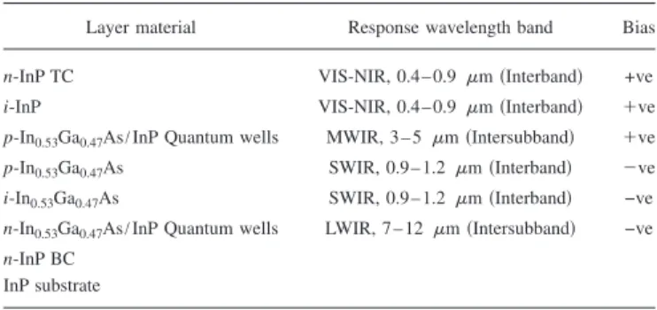
The interband 共VIS-NIR兲 spectral cross-talk observed for the GaAs-based n-p-n-QWIP can be reduced using a
ma-terial system such as In0.53Ga0.47As/ InP in an n-p-n-QWIP
structure. Specific elements in an In0.53Ga0.47As/ InP-based
n-p-n-QWIP structure and corresponding spectral bands
ex-pected from these elements are shown in TableI. Since light
at wavelengths below 0.9 m will be absorbed in the top
InP layers, the i-In0.53Ga0.47As layer will respond to light
only in the 0.9– 1.7 m range 共1.7 m corresponds to the
band gap of In0.53Ga0.47As兲. The VIS-NIR and MWIR bands
can be selected using a positive bias on the top contact, while the SWIR and LWIR bands can be selected using a negative bias on the top contact.
In summary, a bias-selectable multicolor detector was demonstrated based on a GaAs-based n-p-n-QWIP. A
four-band n-p-n-QWIP detector using the In0.53Ga0.47As/ InP
ma-terial system was also proposed. This work was supported, in part, by the U.S. Air Force, under the STTR Contract Nos. FA9550-09-C-0106 and FA9550-10-C-0131, and the Georgia Research Alliance.
1A. Rogalski, J. Antoszewski, and L. Faraone,J. Appl. Phys.105, 091101
共2009兲.
2G. Ariyawansa, P. V. V. Jayaweera, A. G. U. Perera, S. G. Matsik, M.
Buchanan, Z. R. Wasilewski, and H. C. Liu,Opt. Lett. 34, 2036 共2009兲.
3A. Majumdar, K. K. Choi, J. L. Reno, and D. C. Tsui,Appl. Phys. Lett.
86, 261110 共2005兲.
4G. Ariyawansa, V. Apalkov, A. G. U. Perera, S. G. Matsik, G. Huang, and
P. Bhattacharya,Appl. Phys. Lett. 92, 111104 共2008兲.
5H. C. Liu, M. Gao, J. McCaffrey, Z. R. Wasilewski, and S. Fafard,Appl.
Phys. Lett. 78, 79 共2001兲.
6G. Ariyawansa, A. G. U. Perera, G. Huang, and P. Bhattacharya, Appl.
Phys. Lett. 94, 131109 共2009兲.
7G. Ariyawansa, M. B. M. Rinzan, D. G. Esaev, S. G. Matsik, G. Hastings,
A. G. U. Perera, H. C. Liu, B. N. Zvonkov, and V. I. Gavrilenko,Appl.
Phys. Lett. 86, 143510 共2005兲.
8R. C. Jayasinghe, G. Ariyawansa, N. Dietz, A. G. U. Perera, S. G. Matsik,
H. B. Yu, I. T. Ferguson, A. Bezinger, S. R. Laframboise, M. Buchanan,
and H. C. Liu,Opt. Lett. 33, 2422 共2008兲.
9S. Krishna, D. Forman, S. Annamalai, P. Dowd, P. Varangis, T. Tumolillo,
Jr., A. Gray, J. Zilko, K. Sun, M. Liu, J. Campbell, and D. Carothers,
Appl. Phys. Lett. 86, 193501 共2005兲.
10S. V. Bandara, S. D. Gunapala, J. K. Liu, S. B. Rafol, C. J. Hill, D. Z. Y.
Ting, J. M. Mumolo, T. Q. Trinh, J. M. Fastenau, and A. W. K. Liu,Appl.
Phys. Lett. 86, 151104 共2005兲.
11E. Smith, L. Pham, G. Venzor, E. Norton, M. Newton, P. Goetz, V.
Ran-dall, A. Gallagher, G. Pierce, E. Patten, R. Coussa, K. Kosai, W. Radford, L. Giegerich, J. Edwards, S. Johnson, S. Baur, J. Roth, B. Nosho, T. De
Lyon, J. Jensen, and R. Longshore,J. Electron. Mater. 33, 509 共2004兲.
12H. Schneider and H. C. Liu, Quantum Well Infrared Photodetectors:
Phys-ics and Applications 共Springer, New York, 2007兲.
TABLE I. Active elements in an In0.53Ga0.47As/ InP-based n-p-n-QWIP.
Layer material Response wavelength band Bias
n-InP TC VIS-NIR, 0.4– 0.9 m 共Interband兲 +ve
i-InP VIS-NIR, 0.4– 0.9 m 共Interband兲 ⫹ve
p-In0.53Ga0.47As/ InP Quantum wells MWIR, 3 – 5 m 共Intersubband兲 ⫹ve p-In0.53Ga0.47As SWIR, 0.9– 1.2 m 共Interband兲 ⫺ve i-In0.53Ga0.47As SWIR, 0.9– 1.2 m 共Interband兲 −ve n-In0.53Ga0.47As/ InP Quantum wells LWIR, 7 – 12 m 共Intersubband兲 −ve n-InP BC
InP substrate
231102-3 Ariyawansa et al. Appl. Phys. Lett. 97, 231102 共2010兲