Chiral Spin Textures and Dynamics in
Multi-Sublattice Magnetic Materials
by
Lucas Marcelo Caretta
B.S. Materials Science and Engineering, University of Minnesota (2013) Submitted to the Department of Materials Science and Engineering
in partial fulfilment of the requirements for the degree of Doctor of Philosophy in Materials Science and Engineering
at the
MASSACHUSETTS INSTITUTE OF TECHNOLOGY June 2019
© Massachusetts Institute of Technology 2019. All rights reserved.
Author . . . Department of Materials Science and Engineering
September 12, 2014
Certified by. . . Geoffrey S. D. Beach Professor, Co-director, Materials Research Laboratory (MRL)
Thesis Supervisor
Accepted by. . . Donald R. Sadoway Chairman, Department Committee on Graduate Students
5
Magnetic Materials
by
Lucas Marcelo Caretta
Submitted to the Department of Materials Science and Engineering on April 26th, 2019, in Partial Fulfillment of the
Requirements for the Degree of
Doctor of Philosophy in Materials Science and Engineering
ABSTRACT
Spintronics is a research field that aims to understand and control magnetic spins on the nanoscale and should enable next-generation data storage and logic. A promising approach is to encode bits of information using nanoscale spin textures, such as chiral domain walls or skyrmions that can be translated by currents across racetrack-like wire devices. One technological and scientific challenge is to stabilize small spin textures and to move them efficiently with high velocities, which is critical for dense, fast memory. For the past decade, work has focused on using ferromagnetic heterostructures to host chiral spin textures. However, ferromagnets have fundamental limitations that inhibit further progress: large stray fields limit bit sizes and precessional dynamics limit operating speeds. In this thesis, we examine a broader class of multi-sublattice materials: ferrimagnets. We show that by using ferrimagnets, the fundamental limits of ferromagnets can be overcome, realizing order-of-magnitude improvements in both size and speed. Using metallic, ferrimagnetic Pt/Gd44Co56/TaOx films with a sizeable Dzyaloshinskii–Moriya
interaction (DMI), we realize a current-driven domain wall motion of 1.3 km s–1 near the angular momentum compensation temperature and room-temperature-stable skyrmions with diameters close to 10 nm near the magnetic compensation temperature. For the first time, we show that the DMI is present in ferrimagnetic insulator garnet films and that the DMI necessitates a rare-earth ion in the magnetic insulator. Thickness dependent studies and interface engineering show that the DMI manifests at the ferrimagnetic insulator – substrate oxide interface. We use a large spin-orbit torque from a Pt overlayer and the DMI to exploit ferrimagnetic dynamics, driving domain walls in low-damping and low-pinning GGG/TmIG/Pt heterostructures at velocities as high as 2.1 km s–1. Moreover, by utilizing the ultra-low damping nature of Bi-YIG and an in-plane field, we can drive domain walls in GSGG/Bi-YIG/Pt at near relativistic velocities exceeding 4.0 km s–1, where the domain wall velocity is no longer limited by a velocity plateau defined by the in-plane field, but the magnon group velocity in Bi-YIG. These results show that multi-sublattice ferrimagnetic films are a promising materials system for next-generation data storage, paving a path forward for the field of spintronics.
Thesis supervisor: Geoffrey S. D. Beach
7
8
Coming to MIT to complete a PhD has been the most rewarding experience of my life. And it has been because of the people. Here, I would like to take the opportunity to thank those who have helped me grow as an engineer, a scientist, a thinker, a leader, and as a human.
First and foremost, I would like to show my extreme gratitude to my PhD advisor Professor Geoff Beach. Nearly six years ago, I was determined to join your research group not necessarily for the innovative research but because of you and the amazing people you have cultivated in your group. You kindness, contagious passion, and drive are what inspire me to get in early, leave late, and discover the unknown every day. Thank you for guidance, your patience, and above all, your enthusiasm for what we do. Thank you for pushing me to my limits intellectually and forcing me to be uncomfortable. You have made me a better trouble shooter, tinkerer, thinker, and presenter, and have helped me grow and develop my own passions. I could not have asked for a better thesis advisor and mentor.
Secondly, I would like to thank the other members of my thesis committee, Professor Caroline Ross and Professor Kim Kimerling. Thank you for your invaluable feedback, guidance, and direction throughout my PhD. Thank you for pushing me and asking the hard questions. In particular, I would like to thank Professor Ross for giving me the opportunity to collaborate with her group on many occasions and for teaching me all things magnetic oxide.
To David Bono, there’s almost nothing in this PhD that doesn’t have your fingerprints (or solder) on it. I cannot count the number of times you’ve helped me solve problems, helped me repair equipment, or made me laugh. Your ingenuity and creativity does not go unnoticed. Thank you for being patient with me with everything you taught me. Thank you for always going above and beyond to make help me design the best measurements systems imaginable. I will always remember what you told me a few years ago while we were designing an experiment in your lab, “Stop thinking like a PhD student and start thinking like an engineer!” Above all, thank you for your friendship. You have helped make this PhD enjoyable, and I can’t wait to grab lunch again. Thank you to Colin Marcus and Brian Neltner for helping me with everything high frequency and LED related along the way. In particular, I want to thank Colin for his friendship and for helping me to design several circuit not only for this thesis but for outreach efforts. Your creativity and willingness to always help does not go unnoticed. Thank you Brian for always being willing to help, always lending an ear, and for all the fun times at lunch.
One of the most valuable things I learned at MIT was how to build and fabricate. I relied heavily on the DMSE machine shops and other MIT shared facilities. I am extremely grateful for the guidance, expertise, and training from Mike Tarkanian. There usually isn’t a thing you don’t know how to build. I would also like to thank Chris Di Perna, not only for machine ship training but for being always willing to talk fitness in the hallway. Thank you, Tara Fadenrecht for always asking how I’m doing and making me laugh in the basement of Building 4. I would also like to thank Shaymus Hudson giving me the tips and trick of the machining world. I would like to sincerely thank Kurt Broderick in EML for sharing his expertise on fabrication, always answering his phone when I need help, and for the great company.
I’ve always loved teaching, and MIT cemented that belief. I would like to particularly thank James Hunter for being patient with me during the photocell lab and helping make that lab enjoyable. I
9 would like to thank Meri Treska and Geetha Berera for letting me learn from their valuable teaching experience. Finally, I would like to thank Professor Harry Tuller for giving me teaching freedom in 3.024 lab.
DMSE would not run without the administrative staff. And I wouldn’t be where I am without them either. I would like to thank Rachel Kemper and Heather Upshaw for gracing me with invaluable opportunities throughout my PhD. In particular, I would like to thank Heather for her support in my entrepreneurial efforts, and Rachel for her guidance with the Lemelson-Vest fund and helping me with the cover artwork. Thank you to Ryan Kendal for the Photoshop help and for always exuberantly saying hi in the hallway! Adam Shervanian - Thanks for countless facilities issues you helped me fix and for your always fast responses. I would also like to thank Department Head, Professor Chris Schuh for always being willing to meet with me and mentor me on numerous occasions. Thank you to Tiffany Luongo for being a great friend and for always keeping the department candy jar protected.
I would like to especially thank DMSE staff Angelita Mireles and Elissa Haverty. Angelita – you have always been there to not only answer my crazy questions, but to be my ally and support system. From when I broke my nose to when I needed a signature, you’ve always been there. I will always appreciate your care. Elissa – Although you’re not the reason I came to MIT, you are certainly one of the reasons I’m glad I came. Forget the ridiculous number of times you helped me with paperwork, I will always value the deep life-long friendship we created. Thank you for always being there when I needed it the most and for helping me survive the past six years.
My PhD has given me the opportunity to travel around the globe. I would like to thank the huge number of international collaborators I’ve had the pleasure of working with, include researchers at MBI-Berlin, TU-Berlin, DESY, BESSY, BNL, ALS, SLS, MPI-Stuttgart, and Mainz.
Being a member of the Beach is an unforgettable experience. Many names and faces have passed through the Beach group and each have had a unique impact on me. To Can Avci, Chi-Feng Pai, Daniel Suzuki, Felix Buettner, Ivan Lemesh, Jason Bartell, Kai Litzius, Kohei Ueda, Liz Rapoport, Mantao Huang, Minae Ouk, Parnika Agrawal, Pooja Reddy, Sara Sheffels, Sarah Schlotter, Sasha Churikova, Seonghoon Woo, Siying Huang, Uwe Bauer, Satoru Emori, and unofficial member Ethan Rosenberg - thank you for always being willing to help and for being my friends and family at MIT. I would like to particularly thank my “incoming class” into the group, AJ Tan and Max Mann. Thanks for all the laughs, memories, and brainstorming sessions. Not only have I learned more from you two than anyone else the past six years, I’ve laughed with you more than anyone. Thanks for the lifelong friendship we’ve created. And remember… “We just do things wrong enough times, we have to get it right eventually…”
This list would not be complete if not for my friends around MIT and around the globe. Thanks to the nanographene conference, comprised of Gregory Eckhian, Brad Nakanishi, Sam Wagstaff, and Cooper Rinzler. I wouldn’t have made it through the first year and written exam without you guys. Thank for the countless late nights studying. See you in Idaho! I would also like to thank my friends outside of MIT – Cam Matheson, Caroline Brantley, Rachael McGillivray, Jamie Berman, Sruti Velamakani, and Kristy Helscel. Thank you for supporting me and believing in me. It has truly meant the world.
10
To Brooke – Thank you for being the unofficial creative director of my thesis and for helping me push through to the end. I wouldn’t have made it without you, and I will always be grateful for that.
Above all, I would like to thank my family. Thank you for your love and support. I owe everything to you. To Nick, Romina, and Marcia - Thanks for being the best older siblings one could ask for. You are my role models and my inspirations. You have taught me more than you know. Thank you for letting me brag about you and for always pretending I’m the smartest sibling.
To my mother, Diana – Thank you for your texts everyday asking if I’m eating well, if I’m sleeping well, and how I’m feeling. Your support and love is all I could ever ask for. You’ve taught me how to be a better human, endure through challenges, and always be the bigger person. Thank you for always pushing me to do my best, celebrating with me during the highs, and being there to help me during the lows. And thank you for tolerating not only one, but two mad scientists in the household.
To my father, Raul – You taught me how to engineer. Thank you for always believing in me and supporting me and my dreams. Thanks for teaching me how to think like engineer and scientist and for helping me forge my own path. From giving me extra math problems as a child to the many late night phone calls problem solving and discussing experiments, you’ve always been there with an open ear to help me grow and learn. Thanks for letting me following in your footsteps.
This work would not have been possible without the financial support of the National Science Foundation Graduate Research Fellowship Program and the National GEM Consortium Fellowship.
11
12
Chiral Spin Textures and Dynamics in Multi-Sublattice Magnetic Materials
1. Acknowledgements ... 7
2. Table of Contents ... 11
3. Background ... 15
3.0 Introduction ... 16
Types of magnetic order ... 16
3.1 Types of Magnetism ... 17
Indirect Exchange ... 22
Magnetism in Metals ... 23
3.2 Magnetic Anisotropy ... 25
3.3 Magnetic Hysteresis Loops ... 29
3.4 Magnetic Domain Walls ... 34
3.5 Dzyaloshinskii – Moriya Interaction and chiral spin textures ... 38
3.6 A brief appendix on magnetic units ... 42
3.7 References ... 44
4. Domain Wall Dynamics and Devices ... 47
4.0 Introduction ... 48
Magnetic Tunnel Junctions (MTJs) ... 48
Hard Disk Drive (HDD) read head- Principles of Operation... 51
MTJ-MRAM ... 53
4.1 Magnetic domain wall devices ... 54
4.2 Domain Wall Dynamics ... 57
Field Driven Domain Wall Motion... 57
Spin Transfer Torque Motion of Domain Walls ... 61
Spin Orbit Torque Motion of Domain Walls ... 64
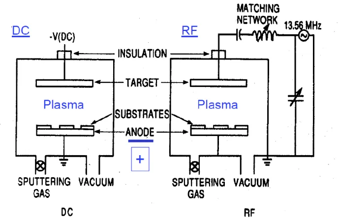
Summary ... 67 4.3 References ... 69 5. Experimental Methods ... 71 5.0 Introduction ... 72 5.1 Material Deposition ... 72 Sputter Deposition ... 72
Pulsed Laser Deposition ... 81
Polycrystalline thin film growth ... 82
5.2 Lithography ... 84
Photolithography ... 84
5.3 Magneto-optical Kerr effect ... 89
Principles of Operation ... 89
In-situ, time-resolved focused MOKE/ MOKE microscope ... 92
Measuring domain wall dynamics ... 94
5.4 Vibrating Sample Magnetometry ... 95
5.5 X-ray imaging ... 96
Scanning x-ray transmission microscopy and X-ray holography ... 97
5.6 Summary ... 99
5.7 References ... 100
6. Measuring and Quantifying the Dzyaloshinskii-Moriya Interaction ... 103
6.0 Introduction and Motivation ... 104
6.1 Asymmetric field-driven expansion of domain walls ... 106
Deriving the DW creep law ... 106
13
Chiral Energy Model of DW Motion ... 109
Dispersive Energy Derivation of Creep Model ... 117
6.2 SOT Dynamics of Domain Wall Motion ... 119
Current driven DW dynamics under an in-plane bias field ... 119
Spin Hall torque magnetometry of chiral DWs ... 120
6.3 Brillouin light scattering (BLS) ... 123
6.4 Summary of methods to measure DMI ... 127
6.5 References ... 128
7. Fast current-driven domain walls and small skyrmions in a compensated ferrimagnet ... 131
7.0 Introduction and Motivation ... 132
7.1 Modeling of the sublattice Ms, i(T) contributions ... 133
7.2 Current pulse profile and velocity calibration ... 134
Pulse Duration ... 135
Domain wall velocity measurement ... 136
7.3 Modeling of ferrimagnetic soliton dynamics ... 137
7.4 Fast domain wall motion near angular momentum compensation ... 139
7.5 Measurement of χ via DC domain wall depinning measurements and field assisted creep ... 141
DC Domain Wall Depinning ... 141
Field Assisted Creep ... 145
7.6 Hall effect measurements ... 145
7.7 Summary of Current Induced Effective Fields ... 149
7.8 One Dimensional Model of a Ferrimagnet ... 151
7.9 Domain wall track heating calibration ... 153
7.10 Realistic modeling of v(j, T) ... 157
7.11 Small DMI skyrmions ... 159
7.12 Holography and Skyrmion Identification ... 165
7.13 Conclusions ... 170
7.14 References ... 172
8. Interface-driven chiral domain walls and their dynamics in magnetic insulating Garnets ... 177
8.0 Introduction and Motivation ... 178
8.1 Current Assisted Domain Wall Motion ... 180
8.2 Thickness Dependence of Micromagnetics Parameters ... 185
8.3 Anomalous Ultra-fast Current-Driven Domain Wall Dynamics in TmIG ... 188
8.4 Relativistic Domain Wall Motion in Bi-YIG ... 193
8.5 Conclusions ... 197
8.6 References ... 199
9. All Optical Motion of Chiral Domain Walls and Skyrmion Bubbles ... 201
9.0 Introduction and Motivation ... 202
9.0 All Optical Domain Wall Motion in High DMI, Co-Rich Pt/Gd14Co86/Ta/Pt ... 203
9.1 All Optical Domain Wall Motion in Gd-Rich Pt/Gd30Co70/Ta/Pt ... 206
9.2 Incoherent DW motion in low DMI, Co-Rich Pt/Gd14Co86/Pt ... 208
9.3 All Optical, High Speed Motion of Skyrmions ... 210
9.4 Conclusions ... 211
9.5 References ... 213
10. Conclusions and Outlook ... 215
15
16
3.0 Introduction
Types of magnetic order
From engineered aluminum welds on automobile frames to color LED displays to corrosion coatings on airplanes, the achievements of materials science and engineering are ubiquitous in the world around us. Lesser known, but equally important, are the ever-present magnetic materials that the world relies on. Magnetic materials are the building blocks of a vast number of applications. Electric car motors, actuators, sensors, headphones, MRI’s, and cybersecurity all rely on advanced magnetic materials. One notable application is high-density data storage. While today, many personal computers and electronic devices rely on electronic forms of memory, magnetic forms of data storage are still the premier choice for dense, inexpensive storage. In fact, “the cloud” relies on such dense forms of storage, including magnetic hard disk drives and even magnetic tape storage. Actually, the most dense forms of memory to-date are magnetic tape and disks, having a capacity of 31 Gbit/cm² (Sony 2017) and 201 Gbit/in² (Seagate 2017), respectively1. Moreover, new, immerging forms of magnetic memory, such as magnetic-RAM (MRAM) aim to outperform and replace current forms of non-volatile memory in personal electronics in the near future.
Our insatiable appetite for more data storage will undoubtedly be met with new materials innovations in magnetic storage, requiring fast, denser, lighter and more power-efficient designs. This thesis aims to make advances to magnetic memory and logic design by exploiting interface-driven chiral effects in multi-sublattice magnetic thin films. This chapter is intended to introduce the reader to the principles of magnetic materials in the context of thin films. Here, we will discuss what gives rise to magnetism, different forms of magnetism, and anisotropic magnetism. We will
17 review domain wall and skyrmion energetics and how domain walls and skyrmions can be used in a device architecture.
3.1 Types of Magnetism
Magnetic moments or “spins” are the fundamental quantized units of magnetism. Magnetism arises when spins order themselves in the absence of a magnetic field. This can take various forms. For instance, when all the magnetic moments lie in the same, unique direction, this is called ferromagnetism2. Although ubiquitous, magnetic order in materials is a purely quantum mechanical phenomenon and cannot be explained by classical physics. Whenever possible, we will describe magnetic behavior using a semi-classical model. The quantum mechanical Hamiltonian for the Heisenberg exchange interaction takes the form of Eq. 3.1.
𝐻̂ = − ∑ 𝐽𝑖𝑗𝑺𝒊∙ 𝑺𝒋 𝑖𝑗
3.1
where 𝐽𝑖𝑗 is the exchange constant, and 𝑺𝒊 and 𝑺𝒋 are adjacent spins. The dot product between the
spins energetically prefers collinear alignment of spins. The exchange energy per unit volume can also be described by
𝐸𝑒𝑥 = 𝐴 (𝛿Θ 𝛿𝑥)
2 3.2
where 𝜃 is the angle between neighboring spins and 𝑥 is the separation between the spins. 𝐴 is a stiffness, often called the exchange stiffness. It is worth noting that magnetic order governed by direct exchange (Eq. 3.1, 3.2) is only possible when the separation distance between neighboring electron spins (𝑥) is very small, such that there is sufficient overlap of their wave function. In the case of a ferromagnet, 𝐽𝑖𝑗 is positive, ensuring parallel alignment of neighboring spins. When 𝐽𝑖𝑗
18
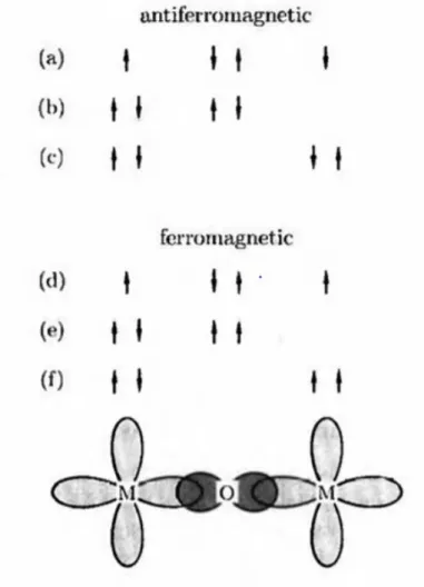
is negative, neighboring spins prefer anti-parallel alignment, giving the system anti-ferromagnetic order. These are schematically shown in Fig. 3.1a,b. The sum of the total magnetic moments in a material per unit volume (or mass) is call the saturation magnetisation (𝑀𝑠). In the case of an antiferromagnet, 𝑀𝑠 = 0, meaning that although magnetic order exists, there is no net magnetisation in the film. Thus, an applied magnetic field has no effect of an antiferromagnet. Crystal structure often dictates if magnetic materials are ferro- or anti-ferromagnetic. For instance, FCC rocksalt structures and monoxides are commonly antiferromagnetic, where alternating 111 planes have oppositely oriented spins.
A third case of magnetic ordering is called ferrimagnetism. In these systems, the magnetic order is anti-ferromagnetic; however, there is still a net moment (see Figure 3.1c). This is often
Figure 3.1 | Types of magnetic ordering. a) ferromagnetism occurs when spins are oriented
along the same direction. Anti-ferromagnetic alignment occurs when spin are oriented anit-parallel. When the net moment is zero, this is an anti-ferromagnet (b), and when there is still a net moment, it is called a ferrimagnet (c).
19 the case in multi-sublattice systems, where different atoms are located on different crystal sites3. Spinel structures are often ferrimagnetic. Two classic ferrimagnet examples are iron oxide Fe3O4 (a spinel) and GdCo (an amorphous metal). In Fe3O4 iron atoms with different valences are found on different sites, giving rise to a net moment. In the case of GdCo, each element occupies a different site2,3. Rare earth- iron garnet materials are another type of ferrimagnet, which take the form: RE3Fe5O12, where RE is a rare earth element. These materials have a cubic crystal structures with a very complicated multi-atom unit cell. Three iron ions are on tetrahedral sites, and two are on octahedral sites, while the Re ions are on sites of dodecahedral symmetry.
The different Curie temperatures of the multi-sublattices yields a non-zero moment that is very temperature-dependent, as each sublattice has its own unique temperature dependence. This can result in one sublattice being dominant at low temperatures and the other being dominant at high temperatures. When the sublattices effectively cancel each other out, the system behaves similarly to a natural anti-ferromagnet. This temperature is called the magnetic compensation temperature. Ferrimagnets have two compensation temperatures. The first is the magnetic compensation, 𝑇𝑀, where the net magnetisation of the film is zero. The second is the angular momentum compensation temperature, 𝑇𝐴, where the net angular moment (the net spin density) of the film is zero. These two compensation points are, in general, not the same temperature, as the lande g-factors, and hence the gyromagnetic ratio of each sublattice might be different (see Eq. 3.3)3.
𝜇 = 𝛾(𝑳 + 𝒈𝑺) 3.3
where 𝜇 = 𝑒/2𝑚 is the magnetic moment, 𝛾 is the gyromagnetic ratio, 𝑒 is the electron charge, 𝑚 is the mass of the electron, 𝑔 is the Lande g-factor, 𝑺 is the spin angular momentum, and 𝑳 is the orbital angular momentum. Eq. 3.3 shows that the total magnetic moment of an electron is the sum
20
of its orbital and spin angular momentum components. The relative amounts of each are weighted by the Lande g-factor. The relationship between the moment and the angular momentum is a function of the gyromagnetic ratio and, hence, the g-factor of each sublattice element. Values for 𝑔 are typically near 2, meaning that the spin angular momentum is about twice as effective in producing a magnetic moment.
Although 𝑳 and 𝑺 are separate quantum numbers, they can be coupled by an effect called spin-orbit coupling, whose Hamiltonian take the form:
𝐻̂ = 𝜉𝑳 ∙ 𝑺 3.4
where 𝜉 ∝ 𝑍4, and 𝑍 is the atomic number. Spin-orbit couple simply means that the spin and orbital angular moments are related to each other. In other words, the bonding or crystal structure of the material will influence the preferred orientation of the moment. Fig. 3.2 illustrates this is a semi-classical way. In Fig 3.2a, a simplistic picture of an atom shows an electron with charge −𝑒 is orbiting the nucleus of an atom of charge +𝑍𝑒, with a velocity 𝑣. Figure 3.2b shows this same simplified picture, but in the rest frame of the electron. In the rest frame of the electron, the +𝑍𝑒 charged nucleus is orbiting an electron with velocity – 𝑣. A moving charge current (the nucleus) generates a magnetic field, similar to a current-carrying wire. Effectively, the movement of the electron in its orbital (dictated by bonding and crystal structure) produces a magnetic field which influences the net moment of the electron. This is spin-orbit coupling. Also noticeable is that the larger the charge of the nucleus, the large the “current,” and the larger the effective magnetic field, implying that heavier elements have larger spin-orbit coupling.
21 Magnetic order only occurs at sufficiently low temperatures. Above a critical temperature, spontaneous magnetic order no longer exists. This critical temperature is call Curie temperature in ferromagnets and the Néel temperature in anti-ferromagnets2. Ferromagnets are the most predominantly used in technological applications however, ferrimagnets are used in some high frequency applications. Many ferrimagnets are electrically insulting with very low magnetic damping. Their insulating properties imply that no eddy current are generated in large oscillating fields. Solids ferrite cores are used in a variety of high frequency applications such as aerials and
transformers requiring high permeability. It has long been thought that anti-ferromagnets and ferrimagnets are not of great use in memory technology, but what we will find is that their near zero magnetisation and vanishing angular momentum make them prime candidate materials for information and data storage technologies.
Figure 3.3 | a) Simplified schematic of an atom in the rest frame of the nucleus and b) in the rest
frame of the electron. In the rest frame of the electron, the motion of the nucleus looks like a magnetic field acting on the electron’s magnetic moment.
22
Indirect Exchange
Many of the ionic oxides in the previous section have antiferromagnetic ordering that does not occur through direct exchange. In particular, there is no direct overlap of neighboring electron orbitals in garnet oxides and fluorides. Instead, the exchange interaction is mediated through a third, non-magnetic ion in a long-range process called super-exchange. This type of order is the ground state, as there is a kinetic energy advantage for antiferromagnetic order in the material.
Figure 3.4 | Super exchange in an iron oxide. Antiferromagnetic coupling between the
Fe, as in (a), (b), (c), the ground state (a) can mix with excited states (b), (b), delocalizing electrons. Ferromagnetic coupling of the two Fe ions, where (d) is the ground state and (e) and (f) are excited states cost energy, as these are prevents by the Pauli exclusion principle.
23 This can be understood by the schematic shown in Fig. 3.4, where Fe ion exchange is mediated by an oxygen ion. In this model, each Fe ion has one unpaired election in a d orbital and the oxygen ion has two unpaired electrons in a p orbital. Antiferromagnetic coupling between the Fe ions allows these outermost electrons to become more delocalized, thus lowering the energy of the system.
Magnetism in Metals
Magnetic ordering in metallically bonded materials does not follow same model as ionically bonded magnetic materials or oxides. In metallic materials, magnetism arises from band ferromagnetism, where magnetic order occurs from spontaneous splitting of electron bands. This can be readily described by examining the rigid band model for the density of states of electrons (see Fig. 3.5a), where spin-up and spin-down electrons are plotted independently2. In the rigid band model, the density of states of transition metal elements is assumed to remain unchanged across the transition metals and alloys of transition metals, the s and d bands are assumed to remain “rigid’ with increasing atomic number. Here, s- (free electron) and d- (localized electron) bands are represented by the local- and free electron-like bands shown in Fig. 3.5a. This model allows us to explain ferromagnetism by simply moving the Fermi energy according to the number of electrons present in the transition metal. Spontaneous magnetism occurs because there is an energetic gain by having an uneven number of spin-up and spin-down electrons; however, this gain must be greater than the kinetic energy cost of moving spins from one sub-band to the other.
From Fig. 3.5a, we can estimate the kinetic energy cost as the energy is takes to move an infinitesimally small amount of minority spin electrons to the majority spin band. This kinetic energy cost is the area of the area of the infinitesimally small sliver multiplied by the Bohr magneton 𝜇𝐵:
24
Δ𝐸𝐾𝐸 = 𝜇𝐵1
2𝑔(𝐸𝑓)𝛿𝐸
3.5
where 𝑔(𝐸𝑓) is the density of states and 𝛿𝐸 is the sliver of electrons. The total magnetic moment 𝑀 is the imbalance of spin up and spin down elections:
M = 𝜇𝐵(𝑛𝑢𝑝 − 𝑛𝑑𝑜𝑤𝑛) 3.6
where 𝑛𝑢𝑝 and 𝑛𝑑𝑜𝑤𝑛 are the number of up and down electrons. Combining Eq. 3.5 and 3.6, we get the following for the kinetic energy cost in terms of the magnetisation:
ΔEKE =1 4
𝑀 𝜇𝐵𝛿𝐸
3.7
The exchange energy gain from having collinear alignment of spins, moving electrons from one spin subband to the other, is
ΔEEx = 𝑈𝑒𝑥𝑛𝑢𝑝𝑛𝑑𝑜𝑤𝑛− 𝑈𝑒𝑥(𝑛 2) (
𝑛 2)
3.8
where 𝑈𝑒𝑥 is the exchange energy and 𝑛 is the total number of electrons. The first term describes the energy of unequal amounts of spin up and spin down electrons, and the second term describes the energy of equal numbers of spin up and spin down electrons. This can be rewritten in terms of the net magnetisation, Eq. 3.6,
ΔEEx= −𝑈𝑒𝑥
4𝜇𝐵2 𝑀
2 3.9
The total energy is then just the sum of the energy cost and gain, ΔEtotal = ΔEEx+ ΔEKE = 𝛿𝐸
4𝜇𝐵𝑀[1 − 𝑈𝑒𝑥 𝑔(𝐸𝐹)]
25 Eq. 3.10 is known as the Stoner criterion3 for ferromagnetism in metal. When the total energy is negative, then spontaneous magnetism occurs. If 𝑈𝑒𝑥 is zero, then there is no net magnetisation. Eq. 3.10 also tells us that the larger the density of state at the fermi level, the larger the energy gain there is for having an imbalance of spins. Looking at the band structure in Fig. 3.5, this is most noticeable if the fermi energy lies in the local d-band of the metal. Using the rigid band model, we can fill electrons from lowest energy states to highest energy states, as we move down the transitions metals and the ones with the Fermi level in the d-band have a higher likelihood of ferrimagnetism. Figure 3.5b shows the Slater-Pauling curve4–6, which illustrates the magnetic moment per atom of various magnetic allows. The peak in the curve occurs for transition metals with large density of states at the Fermi level (Co,Ni,Fe).
Figure 3.5 | a) Density of states for minority and majority spin bands. Band splitting occurs
when there is a greater energetic gain from parallel alignment of spins. b) Slater-Pauling curve showing a larger magnetic moment for transition metals with large density of states at the Fermi level.
3.2 Magnetic Anisotropy
In the previous section, we discussed how magnetic order arises in a material; however, we have not said anything about the preferred direction the co-linear spins prefer to align. Magnetic
26
anisotropy is the preference of the magnetic moment of a material to lie along a certain direction(s). As we will find out shortly, magnetic anisotropy is one of the most powerful properties of a magnetic material. It affects the stability of magnetic bits in memory application, the size of spin textures, how magnetic domain walls and skyrmions move, the shape of hysteresis loops, and much more. It is one of the most engineered parameters in magnetism. Large or small anisotropy and the types of anisotropy needed depend on the application. Here, we will consider where anisotropy arises in thin film magnetic systems, which can be dramatically different from bulk systems.
In thin film systems, magnetic anisotropy can come from a variety of sources. Perhaps, the easiest to understand in shape anisotropy, which, as its name eludes, comes from the shape of a magnetic material. Different amounts of free magnetic poles can form at the surfaces of materials, resulting in stray field or demagnetizing field it produces, as this raises the total energy of the system. Stray fields are a “long-range’ magnetic interaction, so the magnetic material can essentially “sense” the edges of the material. A magnetic material will, in general, tend to minimize the stray field it produces. In other words, it follows Maxwell’s equations and tries to minimize the divergence of the magnetisation (∇ ∙ 𝐌). This will cause the magnetisation to point along the long axis of a material, minimizing free poles. Magnetostatic energy is the term used to describe the energy resulting from stray fields or the shape of a material, and take the form:
Ed = −1
2𝑀 ∙ 𝐻𝑑
3.11
where 𝐻𝑑 is the demagnetizing field and is related to the magnetisation of the film, 𝑀, 𝐻𝑑 = −𝑁𝑀, where 𝑁 is a demagnetizing tensor that depends on the shape of the material. Calculating 𝑁 is not trivial. In the case of a thin film, the film extends infinitely in two dimensions and is tightly constrained in the third dimension. The resulting demagnetizing energy for a thin film is:
27 𝐸𝑑 = − 1
8𝜋𝑉∫ 𝑀𝐻𝑑𝑑𝑣 = 2𝜋𝑀𝑠
2cos2𝜃 3.12
where 𝑉 is the volume of the film, 𝑑𝑣 is a volume element, and 𝜃 is the angle between the magnetisation and the film normal. Eq. 3.11 agrees with intuition, and energy is minimized when the magnetisation of the film lies in the plane of the film. We will call this in-plane magnetization or IP for short.
Dipolar or shape anisotropy is not the only factor that dictates a material’s anisotropy in a thin film. Ultra-thin films have many properties that are dictated by the breaking of symmetry caused by interfaces8. Shape anisotropy tells us that a thin film would prefer to have its magnetisation lie in the plane of the film. However, in 1954 Néel predicted the existence of surface
Figure 3.6 | Total anisotropy 𝑘𝑒𝑓𝑓 as a function of Co layer thickness. The fit to the data (line) is a linear fit described in Eq. 3.13, where the slope of the line describes the volume contribution to anisotropy 𝑘𝑣 and the y-axis intercept describes the surface contribution 𝑘𝑠. Image taken from ref7
28
anisotropies that could change the preferred axis of orientation (or easy axis) of a film9. This was later confirmed in experiments, and notable it was discovered later that Pt/Co10 and Pd/Co10,11 magnetic multilayer thin films grow in a particular orientation (111) caused the easy axis of the material to be perpendicular to the plane of the film, so called perpendicular magnetic anisotropy (PMA). This can be seen in Fig. 3.67, which plot the total anisotropy of a film 𝑘𝑒𝑓𝑓 as a function of Co thickness 𝑑 in Pd/Co multilayers. In this plot, when 𝑘𝑒𝑓𝑓 is positive the film has PMA and when it is negative it has in-plane magnetisation. Using Fig. 3.6, we can separate out the volume anisotropy effects from the surface (PMA) effects by fitting the line to the following expression10,11:
𝑘𝑒𝑓𝑓 = 𝑘𝑣 +𝑘𝑠 𝑑
3.13
where 𝑘𝑣 is the volume anisotropy and 𝑘𝑠 is the surface anisotropy. Below a certain thickness of Co (𝑑𝑠𝑟𝑡), the magnetisation will reorient itself to an out-of-plane orientation. This is the so-called spin-reorientation transition. Dipolar and strain are the main contributions to the volume anisotropy term, while spin-orbit coupling is mainly responsible for the surface term in Eq. 3.13. Since spin-orbit coupling describes the coupling between electron orbitals and their spin orientation, it is only natural that bonding or the crystal structure of a film plays a large role in its magnetic anisotropy.
Magnetic anisotropy is a vital parameter in the design of data storage. Anisotropy is the key metric which sets the standard for memory lifetimes. The energy barrier of magnetisation reversal is 𝐸𝑟𝑒𝑣 = 𝑘𝑒𝑓𝑓𝑉 where 𝑉 is the volume of the magnetic bit. A large 𝑘𝑒𝑓𝑓 is necessary to keep the barrier large such that a bit remains stable for along time in the presence of thermal fluctuations. The industry standard for a 10-year lifetime is 𝐸𝑟𝑒𝑣 > 60𝑘𝑏𝑇, where 𝑘𝑏 is the Boltzmann constant and 𝑇 is temperature. As bits become increasingly smaller, more anisotropy
29 is need to keep this figure above 60𝑘𝑏𝑇; however, the energy barrier should be low enough to be able to switch the magnetisation with low energy when needed. The competition between the three industry requirements (small bits, low write energy, and stability) is often referred to as the magnetic recording trilemma.
As we will see in later chapters, perpendicular magnetic anisotropy can also be present in thicker ferrimagnetic allows, such as GdCo, TbCo, FeCo12, and alloys of these materials. This is so-called “bulk perpendicular magnetic anisotropy,” as it does not come from the interface, as in Pd/Co and Pt/Co thin films. The origin of bulk PMA in thin films is not clear. However, in these materials, one can increase their thickness (increase their volume), increasing 𝐸𝑟𝑒𝑣, without having to increase 𝑘𝑒𝑓𝑓, potentially solving one piece of the magnetic recording trilemma.
3.3 Magnetic Hysteresis Loops
Magnetic hysteresis loops are arguably the most powerful way to characterize a magnetic sample. A wealth of information can be gathered from hysteresis loops, including a number of magnetic and material properties. In a hysteresis loop, the magnetic field is swept in one direction, while the magnetisation of the film in that same direction is measured. A variety of techniques outlines in Chapter 5 can be used to measure the magnetisation of the sample during the field sweep. The amount of energy it takes to orient a magnetic moment in a particular direction is a strong function of the anisotropy of the film. We will see that the type of magnetic anisotropy will have an impact on the shape of the hysteresis loop. By this, we can also determine the strength of the anisotropy of magnetic material. For this thesis, we will only consider the case where there is one single easy axis of preferred magnetisation. This is called uniaxial anisotropy and can be used to describe all magnetic materials in this thesis.
30
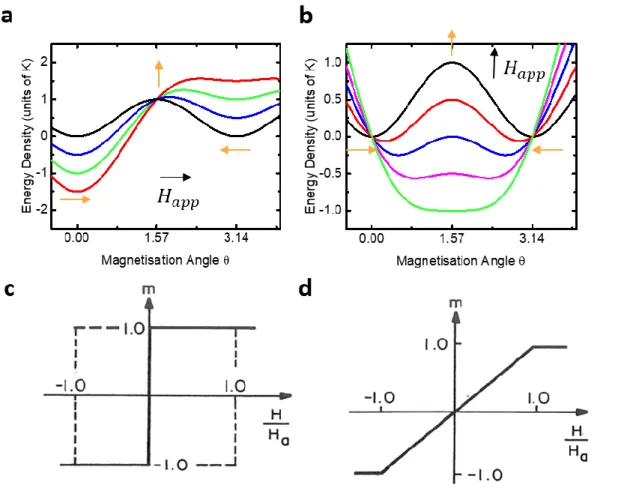
We will use the Stoner Wohlfarth model to describe the magnetisation of a single domain as a function of field. This will allow us to correctly determine the qualitative shapes of hysteresis loops. In the Stoner Wohlfarth, the total energy of the system is described by the sum of the energy due to the applied magnetic field (Zeeman energy) and the anisotropy energy. The energy landscape of uniaxial anisotropy can be described by2
𝐸𝑢𝑛𝑖 = 𝐾𝑠𝑖𝑛2(𝜃) 3.14
where 𝐾 is the uniaxial anisotropy constant, and 𝜃 is the deviation of the magnetisation from the easy axis. The Zeeman energy from a field acting on a magnetic moment is equal to2
𝐸𝑍𝑒𝑒𝑚𝑎𝑛 = −𝑀𝑠𝐻𝑐𝑜𝑠(𝜃′) 3.15
where 𝜃′ is the angle between the magnetisation and the applied field. The total energy is equal to the sum of Eq. 3.14 and 3.15. The anisotropy energy landscape is plotted as a function of the angle 𝜃 in Fig. 3.7a. Here, we clearly see the degenerate easy axis along 0 and 𝜋 radians, and a hard axis along 𝜋
2. Let’s take a scenario where the magnetisation is current pointed along the 𝜃 = 𝜋 direction. When a magnetic field is applied along the easy axis, say 𝜃 = 0 radians, the energy landscape shifts, as the Zeeman energy begins to contribute, lowering the energy of the 𝜃 = 0 states and raising the energy of the 𝜃 = 𝜋 state. However, the horizontal position of the minimum does not change. As the field increases, the local minimum continue to shift vertically, but not horizontally on the plot, as indicated by the colored lines in Fig. 3.7a for various applied fields. When the 𝜃 = 𝜋 state is within 𝑘𝑏𝑇 of the maximum, then the magnetisation switches directly from 𝜃 = 𝜋 to 𝜃 = 0, the new preferred energy state. If we instead plot the magnetisation along the magnetic field direction 𝑀𝑥 as a function of the field, this yields a square easy axis magnetic hysteresis loop (Fig. 3.7c2).
31 The story changes considerably if we now consider the case where we apply a magnetic field along the hard axis 𝜃 =𝜋
2. Here, the 𝜃 = 𝜋
2 state lowers in energy, while the 𝜃 = 0, 𝜋 states rise in energy (vertical shift), but there is also a horizontal shift of these minimum, which continues as we increase the hard axis applied field. This is show in Fi. 3.7b for various hard axis fields. Finally, when the magnetic field is strong enough the magnetisation is forces along its hard axis, 𝜃 =𝜋
2. If instead, we plot the magnetisation along the hard axis (𝜃 = 𝜋
2), we see a linear dependence of the magnetisation on field, until the moment is saturated along the hard axis (Fig 3.7d2).
Figure 3.7 | Energetics a) easy axis and b) hard axis loops as a function of 𝜃, the angle between the magnetisation and the easy axis. Resulting c) easy and d) hard axis hysteresis loops. c,d) adapted from ref2.
32
From Fig 3.7c,d, we can define many magnetic material properties: the saturation magnetisation 𝑀𝑠, the remnant magnetisation 𝑀𝑟, the coercivity 𝐻𝑐, and the anisotropy field 𝐻𝑘. The coercive field 𝐻𝑐 is given by the 𝑀 = 0 crossing of the easy axis loop, ie- the field at which the magnetisation switches. The remnant magnetisation 𝑀𝑟 is the 𝐻 = 0 intercept of the loop, ie- the magnetisation that remains when the field is turned off. A common measure of the sqaureness of a hysteresis loop is 𝑀𝑟/𝑀𝑠. An easy axis loop has an
𝑀𝑟
𝑀𝑠 of 1, while for a hard axis loop, it is 0.
Any loop in-between these two angles gives a value of 0 <𝑀𝑟
𝑀𝑠 < 1. For magnetic memory
application, uniaxial anisotropy is useful. There are two distinct magnetisation levels depending on the prior magnetisation state of the sample. This is a binary system, and the up or down state can reflect a 1 or 0 bit of information.
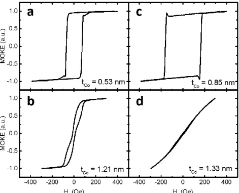
Fig. 3.8 brings together both the concepts of interface anisotropy and magnetic hysteresis loops. Various out of plane magnetic hysteresis loops are plotted for a thin film system of Ta(4 nm)/Pt(3 nm)/Co(𝑡𝐶𝑜)/Oxide(8 nm). We have varied the Co layer thickness 𝑡𝐶𝑜 between approximately 0.5 and 1.3 𝑛𝑚. The Ta layer serves as an adhesion layer between the Si/SiO2 substrate and the Pt. The purpose of the oxide cap is to protect the Co layer from oxidation in the atmosphere. The hysteresis loops are obtained using a technique called the magneto-optical Kerr effect, which will be describe in detail in Chapter 5. The y-axis units represent the fraction of magnetisation out of the plane of the sample. As one can see, at 𝑡𝐶𝑜 = 0.85 𝑛𝑚 the hysteresis loops is square, indicating the easy axis of the film is out of the plane (PMA). Here, surface anisotropy dominates. At very large 𝑡𝑐𝑜 = 1.33 𝑛𝑚, the sample hysteresis loop appear to resemble a hard axis loop that is not saturated, meaning that the hard axis is out of the plane and the easy axis is in the plane. Here, volume anisotropy dominates. Between these two thicknesses, 𝑡𝐶𝑜 = 1.21 𝑛𝑚, the loops take a mixed shape, indicating that both surface and volume anisotropy
33 contribute to the total anisotropy. At very thin 𝑡𝐶𝑜 = 0.53 𝑛𝑚, the coercivity 𝐻𝑐 drops slightly. This is an indication that the out of plane anisotropy has dropped slightly. This effects can be attributed to a lack of magnetic material. 0.5 𝑛𝑚 of Co is extremely thin, and there simply isn’t enough magnetic material to retain full anisotropy.
Figure 3.8 | MOKE magnetic hysteresis loops taken on Ta(4 nm)/Pt(3 nm)/Co (𝑡𝐶𝑜)/Oxide(8 nm), where 𝑡𝐶𝑜= a)0.53 𝑛𝑚, b) 0.85𝑛𝑚, c) 1.21 𝑛𝑚 and d) 1.21 𝑛𝑚.
In the Stoner Wohlfarth model 𝐻𝑐 = 𝐻𝑘, but in reality this is almost never the case. 𝐻𝑐 is almost always significantly smaller than 𝐻𝑘. The Stoner Wohlfarth model assume the all the spins in the magnetic material can be modeled by a single vector. This is called the single domain assumption. In reality, switching does not occur by coherent rotation of all moments in a ferromagnet. Instead, magnetic domains nucleated and expand across the sample until it has switched. Domain walls are the finite transition regions between oppositely oriented domains, and will be the focus of the next section 3.4.
34
3.4 Magnetic Domain Walls
So far, we assumed that all moments of a ferromagnetic material are aligned along the same direction; however this is not always the case. In fact, single domained magnets are quite rare. In the last section, we discussed how a magnetic material aligns along its long axis to minimize the divergence of (∇ ∙ 𝐌). A magnetic material can minimize its stray field (minimize its magnetostatic energy) even further by breaking up into differently oriented regions called magnetic domains (see Fig. 3.9a,b), such that the material is demagnetized, where the net magnetisation of a demagnetized material is zero13. There are finite regions between magnetic domains where the magnetisation smoothly rotates from one direction to another. These thin
regions are called magnetic domain walls. There are two main types of magnetic domain walls in
Figure 3.9 | a) uniformly magnetised and b) multidomain magnets. Breaking up into domains
35 thin films materials. In other words, there are two preferred ways that the magnetisation prefers to rotate from one domain to the next: Bloch domain walls and Néel domain walls. In a Bloch domain wall, the magnetic moment rotates perpendicular to the domain wall normal vector. In a Néel domain wall, it rotates parallel to the domain wall normal. These are schematically shown in Fig. 3.9c,d.
The formation of magnetic domain walls actually costs energy, as magnetic moments in the domain wall no longer lie along the easy axis of the material. The energy cost of forming a Bloch magnetic domain wall 𝜎𝐵 is a function of the anisotropy energy of the film 𝐾 and the exchange constant 𝐴3.
𝜎𝐷𝑊= 𝜋√𝐴𝐾 3.15
Although domain walls cost energy, they spontaneously form in magnetic materials as they greatly reduces the demagnetizing field in the ferromagnet (see Fig. 3.9a,b). Domain walls also have a finite width Δ, which is also dependent on 𝐴 and 𝐾3.
Δ = √𝐴/𝐾 3.16
In expression 3.16, the anisotropy competes with the exchange stiffness. The exchange stiffness prefers a wide, infinitely large, domain walls, as this keeps more moments in the domain wall to be closer to parallel aligned. The anisotropy prefers an infinitesimally small domain wall, as this keeps more moments along the easy axis of the film.
Néel walls are more common in materials whose domain wall width is larger than the thickness of the film and the lithographically patterned magnetic track. Bloch walls are more common in films where the domain wall width is larger than the thickness of the film, but smaller than the width of the magnetic track. This can be seen schematically in Fig. 3.10. The domain wall itself, represented by a white rectangle in Fig. 3.10, can be thought of as magnet itself. The Bloch
36
wall in Fig. 3.10a would produce less demagnetizing field than the Néel domain wall in Fig. 3.10b, as the magnetisation of the Bloch wall lies along the long axis of the domain wall “rectangle” in the very wide track in Fig. 3.10a,b. The narrow track in Fig. 3.10c,d would favor a Néel domain wall, as the long axis of the domain wall “rectangle” lies along the domain wall normal. In a typical PMA, the width of a domain wall is typically tens of nanometers and the width of the magnetic trackis almost always several hundred nanometers or more. This geometry is best described by Fig. 3.10a. As a result, Bloch walls are more often observed in magnetic thin films with PMA14.
The domain walls in a multidomain sample are mobile, ie- a multidomain sample can be made uniformly magnetized by driving domain walls into motion. This can be done by applying a magnetic field to the sample. When a magnetic field is applied to the sample, the domain oriented in the same direction of the applied field will grow, while the domains not oriented in the direction of the field will shrink (Fig. 3.11). The tendency of a magnet to orient in the direction of the applied field is called the Zeeman Effect, where the Zeeman energy is reduced when the magnetic moment
Figure 3.10 | a) Bloch and b) Néel domain walls in thin film patterned into a wide track. Bloch
walls are energetically e preferred here. c) Bloch and d) Néel walls patterned in a thin film patterned into a narrow track. Here, Néel walls are energetically preferred.
37 is aligned with the field. The dynamics of the motion of the domain wall under an applied field will be discussed in the next chapter.
Figure 3.11 | Magnetic domain walls in a multidomain sample.
When a magnetic field is applied, the domain oriented in the direction of the applied field will grow, while the domain oriented in the opposite direction will shrink.
The difference between a multidomain material and a multidomain material is also the reason why some materials are permanent magnets and other are not. For example, a nail would stick to your refrigerator, but nails don’t typically stick to each other. This is because the magnet in the refrigerator is a single domain magnet with large stray fields, while the nail is a multidomain material. If you bring a nail close to your refrigerator, the magnetic field produced by the single domain magnet in your refrigerator will cause the domain walls in the nail to move until the nail itself becomes single domain. Once the nail is single domain, the stray field produced by the nail and the refrigerator will cause them to attract to one another. Once the nail is pulled away from
38
the refrigerator the domain walls will spontaneously reform. If you brought two nails together they would not be attracted to each other, since they are multidomain and have very small stray fields.
In some materials, domain walls can become pinned or “stuck” after the field is removed. This occurs when there is a local energy well for the domain wall to be pinned on. This can be a change in anisotropy 𝐾, magnetisation 𝑀𝑠, or even exchange stiffness 𝐴. Practically, this is a grain boundary, surface roughness, voids, or even a scratch of the surface of the material.
Note that when a domain wall or other spin textures such as skyrmions (to be discussed later) “move” in a material, no physical motion actually occurs. Magnetic domain walls are quasi-particles, meaning they aren’t physical objects, but can be conveniently regarded as objects. Quasi-particles have properties that are characteristic of objects, like momentum, size, energy, and shape. They also can interact with one another like particles do. For instance, the carbon dioxide bubbles in sparkling water themselves are not particles, as they are just the displacement of water by CO2. But the bubble itself (the absence of water) has properties similar to a particle. Bubbles can interact with each other, they float, etc. Another analogy, more similar to domain walls or skyrmions are the pixels on your cellphone screen. When watching a video of a moving car on your screen, the car itself isn’t moving, but the pixels on the screen are changing colors giving the appearance of a moving car. This is similar to local electron spins in a material. The spins themselves aren’t moving, however their rotation gives rise magnetic objects that can be treated as particles. For example, domain walls can be pinned and they interact with each other.
3.5 Dzyaloshinskii – Moriya Interaction and chiral spin textures
The Heisenberg exchange interaction introduced in this chapter energetically prefers collinear alignment of magnetic spins. This is explicitly written in terms of the Hamiltonian in Eq.
39 3.1. In some materials, a different type of exchange interaction, the asymmetric exchange interaction, is present. The asymmetric exchange interaction is also commonly referred to as the Dzyaloshinskii-Moriya interaction (DMI), named after the two physicists who predicted its existence. The DMI has a Hamiltonian of the form15,16:
𝐻̂ = − ∑ 𝐷𝐷𝑀𝐼 𝑖𝑗𝑺𝒊× 𝑺𝒋 𝑖𝑗
3.17
where 𝐷𝑖𝑗 is the DMI tensor, and 𝑆𝑖, 𝑗 are adjacent magnetic spins in a material. The DMI manifests itself in materials whose structure lack inversion symmetry. The cross product prefers perpendicular alignment of these adjacent spins rather than collinear alignment. When both the Heisenberg exchange interaction and the DMI are significant in a material, magnetic twists and spiral can form. 𝐷𝑖𝑗 is also a chiral tensor, meaning it is not symmetric. Thus, spin textures that
form have preferred handedness or chirality. We will find that this greatly impacts both the statics and dynamics of spin textures. There are two main ingredients to manifest DMI in a material: large spin-orbit coupling and broken inversion symmetry15,16. The DMI is actually an indirect exchange interaction that is mediated through an element of large spin-orbit coupling. The DMI was first
Figure 3.12 | a) Bulk and b) interfacial DMI manifesting in bulks and thin film systems,
respectively. The DMI is mediated through an element of large spin-orbit coupling. Adapted from ref17
40
experimentally observed in bulk materials whose crystal structure lacks inversion symmetry, such as the B20 system. Fig. 3.12a17 schematically illustrates the indirect DMI resulting in bulk materials, commonly referred to as “bulk DMI.”
Chiral magnetic structures resulting from bulk DMI have been observed in MnW18, FeMn19, MnSi20,21, FeGe22, Fe1-xCoxSi23, and La2Cu0.97Li0.03O424 systems. Until recently, chiral spin textures stabilized by the DMI had only been observed in single crystal B20 systems under cryogenic temperatures. However, it was discovered that interfaces between materials can also provide the necessary inversion asymmetry needed to manifest the DMI. Moreover, the same heavy metals that give rise to PMA in thin films systems also provide the large spin-orbit coupling for the DMI. Emori et al25 and Ryu et al26 separately discovered homochiral Néel domain walls at room temperature in Pt/Co(Fe)/Oxide films. This type of DMI is often called interfacial DMI, and is schematically described in Fig. 3.12b17, where the asymmetric exchange between adjacent spins in mediated via the heavy metal in the adjacent underlayer. A pair homochiral Néel walls are
Figure 3.13 | a) A pair of right handed homochiral Néel domain walls. b) Bloch and c) Néel
41 shown in Fig. 3.13a. Notice that the magnetisation in the domain wall always rotates clockwise moving from wither an up to down domain or a down to up domain.
The discovery of interfacial DMI manifesting in room-temperature systems has sparked a remarkable amount of research in chiral magnetic systems and the different spin textures that evolve in these chiral systems. The most frequently studied are magnetic skyrmions. A skyrmion is a topologically wound circular spin textures that is defined by its winding number, which is the total number of times the spin textures’ moments can be mapped onto a sphere. Two different types of skyrmions form from the DMI, a Bloch skyrmion and a Néel skyrmion. A Bloch skyrmion manifests from the symmetry of bulk DMI and a Néel skyrmion manifests from the symmetry of interfacial DMI. Néel and Bloch skyrmions are shown schematically in Fig. 3.13b,c17, respectively. Similar to domain walls, a Bloch skyrmion’s wall rotates perpendicular to the domain wall normal and a Néel skyrmion’s wall rotates parallel to the wall normal. Another way to visualize skyrmions is simply domain walls wrapped around themselves. These topological “domains” are two-dimensional objects that can be stable down to a few nanometers in size17skyss. Moreover, from their topology, skyrmions exhibit a variety of topological and gyrotropic effects, such as the skyrmion Hall angle27,28 and the topological Hall angle29. Since we only consider interfacial DMI in this thesis, a skyrmion will be assumed to be of Néel type, unless otherwise specified.
Bloch skyrmions have been extensively studied in B20 systems at cryogenic temperatures (Fig. 3.14a) using bulk imaging techniques, such as Lorentz TEM. And recently, room temperature Néel skyrmions have been observed in thin film systems exhibiting interfacial DMI (Fig. 3.14b)30– 32. Like magnetic domain walls, skyrmions have been conceptualized as magnetic bits for information storage. Over the past few years, research efforts have focused on the nucleation,
42
annihilation, and detection of skyrmions and chiral domain walls in thin films. Moreover, ultrafast motion of chiral spin textures has attracted a lot of attention and will be the primary focus of this thesis.
3.6 A brief appendix on magnetic units
Of all the branches of physics and materials science, magnetism has arguably the most confusing system(s) of units. Units are often equated when they should not be, and there is general misconception with the best way to represent these units. SI units are often advantageous because they are popular and adopted by the majority of scientists in the field; however, the Gaussian unit system has the advantage that it simplifies theoretical relations between electromagnetic phenomenon and SI units are often used incorrectly. Throughout this thesis, both SI and Gaussian units will he used. To aid the reader in relating these two, below is a table that summarizes the definitions of and relationships between the various magnetic units. The table below has been adapted from ref33
Quantity Symbol Gaussian & cgs emu a Conversion factor, C b
SI &
rationalized mks c
Magnetic flux density,
magnetic induction B gauss (G)
d
4-Oct tesla (T), Wb/m2
Magnetic flux Φ maxwell (Mx), Gּcm2 8-Oct weber (Wb), volt
second (Vּs) Magnetic potential
difference,magnetomotive force
U, F gilbert (Gb) 10/4π ampere (A)
Magnetic field strength,
magnetizing force H oersted (Oe),
e
Gb/cm 103/4π A/m f
43
(Volume) magnetization 4πM G 103/4π A/m
Magnetic polarization,
intensity of magnetization J, I emu/cm
3 4π x 10-4 T, Wb/m2i
(Mass) magnetization σ, M emu/g 1 Aּm
2/kg
4π x 10-7 Wbּm/kg
Magnetic moment m emu, erg/G 3-Oct Aּm
2, joule per
tesla (J/T) Magnetic dipole moment j emu, erg/G 4π x 10-10 Wbּm i
(Volume) susceptibility χ, κ dimensionless, emu/cm3
4π dimensionless
(4π)2 x 10⁻⁷ henry per meter
(H/m), Wb/(Aּm) (Mass) susceptibility χρ, κρ cm3/g, emu/g 4π x 10
-3 m3/kg
(4π)2 x 10⁻¹⁰ Hּm2/kg
(Molar) susceptibility χm, κmol cm3/mol, emu/mol
4π x 10-6 m3/mol
(4π)2 x 10-13 Hּm2/mol
Permeability μ dimensionless 4π x 10-7 H/m, Wb/(Aּm)
Relative permeability j μ
r not defined - dimensionless
(Volume) energy density,
energy product k W erg/cm
3 1-Oct J/m3
Demagnetization factor D, N dimensionless 1/4π dimensionless
a. Gaussian units and cgs emu are the same for magnetic properties. The defining relation is B = H +
4πM.
b. Multiply a number in Gaussian units by C to convert it to SI (e.g., 1 G x 10-4 T/G = 10-4 T).
c. SI (Système International d’Unitès) has been adopted by the National Bureau of Standards.Where to
conversion factors are given, the upper one is recognized under, or consistent with, SI and is based on the definition B = μo(H + M), where μo = 4π x 10-7 H/m. The lower one is not recognized under SI and
is based on the definition B = μoH + J, where the symbol I is often used in place of J.
d. 1 gauss = 105gamma (γ).
e. Both oersted and gauss are expressed as cm-1/2ּg1/2ּs-1 in terms of base units.
f. A/m was often expressed as “ampere-turn per meter” when used for magnetic field strength. g. Magnetic moment per unit volume.
h. The designation “emu” is not a unit.
i. Recognized under SI, even though based on the defition B = μoH + J. See footnote c.
j. μr = μ/μo = 1 + χ, all in SI. μr is equal to Gaussian μ.
44
3.7 References
1. Sony Storage Media Solutions Corporation. Sony Global - Sony Develops Magnetic Tape Storage Technology with the Industry’s Highest*1 Recording Areal Density of 201 Gb/in2. (2017). Available at: https://www.sony.net/SonyInfo/News/Press/201708/17-070E/index.html. (Accessed: 6th March 2019)
2. O’Handley, R. C. Modern magnetic materials : principles and applications. (Wiley, 2000).
3. Blundell, S. Magnetism in condensed matter. (Oxford University Press, 2001).
4. Balke, B., Wurmehl, S., Fecher, G. H., Felser, C. & Kübler, J. Rational design of new materials for spintronics: Co_2FeZ ( Z =Al, Ga, Si, Ge). Sci. Technol. Adv. Mater. 9, 014102 (2008).
5. Slater, J. C. The Ferromagnetism of Nickel. II. Temperature Effects. Phys. Rev. 49, 931– 937 (1936).
6. Pauling, L. The Nature of the Interatomic Forces in Metals. Phys. Rev. 54, 899–904 (1938).
7. Cullity, B. D. & Graham, C. D. Introduction to Magnetic Materials. (John Wiley & Sons, Inc., 2008). doi:10.1002/9780470386323
8. Johnson, M. T., Bloemen, P. J. H., Broeder, F. J. A. den & Vries, J. J. de. Magnetic anisotropy in metallic multilayers. Reports Prog. Phys. 59, 1409–1458 (1996).
9. Néel, L. Anisotropie magnétique superficielle et surstructures d’orientation. J. Phys. le Radium 15, 225–239 (1954).
10. Carcia, P. F. Perpendicular magnetic anisotropy in Pd/Co and Pt/Co thin‐film layered structures. J. Appl. Phys. 63, 5066–5073 (1988).
11. Carcia, P. F., Meinhaldt, A. D. & Suna, A. Perpendicular magnetic anisotropy in Pd/Co thin film layered structures. Appl. Phys. Lett. 47, 178–180 (1985).
12. Hansen, P. & Heitmann, H. Media for erasable magnetooptic recording. IEEE Trans. Magn. 25, 4390–4404 (1989).
13. Heinrich, B. & Cochran, J. F. Ultrathin metallic magnetic films: magnetic anisotropies and exchange interactions. Adv. Phys. 42, 523–639 (1993).
14. Koyama, T. et al. Observation of the intrinsic pinning of a magnetic domain wall in a ferromagnetic nanowire. Nat. Mater. 10, 194–197 (2011).
15. Dzyaloshinsky, I. & I. A thermodynamic theory of “weak” ferromagnetism of antiferromagnetics. J. Phys. Chem. Solids 4, 241–255 (1958).
16. Moriya, T. Anisotropic Superexchange Interaction and Weak Ferromagnetism. Phys. Rev.
120, 91–98 (1960).
17. Fert, A., Cros, V. & Sampaio, J. Skyrmions on the track. Nat. Nanotechnol. 8, 152–156 (2013).
18. Bode, M. et al. Chiral magnetic order at surfaces driven by inversion asymmetry. Nature
447, 190–193 (2007).
19. Meckler, S. et al. Real-Space Observation of a Right-Rotating Inhomogeneous Cycloidal Spin Spiral by Spin-Polarized Scanning Tunneling Microscopy in a Triple Axes Vector Magnet. Phys. Rev. Lett. 103, 157201 (2009).
20. Mühlbauer, S. et al. Skyrmion lattice in a chiral magnet. Science (80-. ). 323, 915–919 (2009).
45 186602 (2009).
22. Yu, X. Z. et al. Near room-temperature formation of a skyrmion crystal in thin-films of the helimagnet FeGe. Nat. Mater. 10, 106–109 (2011).
23. Yu, X. Z. et al. Real-space observation of a two-dimensional skyrmion crystal. Nature
465, 901–904 (2010).
24. Raičević, I. et al. Skyrmions in a Doped Antiferromagnet. Phys. Rev. Lett. 106, 227206 (2011).
25. Emori, S., Bauer, U., Ahn, S.-M., Martinez, E. & Beach, G. S. D. Current-driven dynamics of chiral ferromagnetic domain walls. Nat. Mater. 12, 611–616 (2013).
26. Ryu, K.-S., Thomas, L., Yang, S.-H. & Parkin, S. Chiral spin torque at magnetic domain walls. Nat. Nanotechnol. 8, 527–533 (2013).
27. Litzius, K. et al. Skyrmion Hall effect revealed by direct time-resolved X-ray microscopy. Nat. Phys. 13, 170–175 (2017).
28. Jiang, W. et al. Direct observation of the skyrmion Hall effect. Nat. Phys. 13, 162–169 (2017).
29. Zeissler, K. et al. Discrete Hall resistivity contribution from Néel skyrmions in multilayer nanodiscs. Nat. Nanotechnol. 13, 1161–1166 (2018).
30. Büttner, F. et al. Dynamics and inertia of skyrmionic spin structures. Nat. Phys. 11, 225– 228 (2015).
31. Woo, S. et al. Observation of room-temperature magnetic skyrmions and their current-driven dynamics in ultrathin metallic ferromagnets. Nat. Mater. 15, 501–506 (2016). 32. Jiang, W. et al. Blowing magnetic skyrmion bubbles. Science (80-. ). 349, 283–6 (2015). 33. R. B. Goldfarb and F. R. Fickett. Magnetic Units. NBS Special Publication 696, U.S.
Department of Commerce, National Bureau of Standards (1985). Available at:
http://ieeemagnetics.org/index.php?option=com_content&view=article&id=118&Itemid= 107. (Accessed: 12th March 2019)
47