HAL Id: hal-00476271
https://hal.archives-ouvertes.fr/hal-00476271
Submitted on 25 Mar 2011
HAL is a multi-disciplinary open access
archive for the deposit and dissemination of
sci-entific research documents, whether they are
pub-lished or not. The documents may come from
teaching and research institutions in France or
abroad, or from public or private research centers.
L’archive ouverte pluridisciplinaire HAL, est
destinée au dépôt et à la diffusion de documents
scientifiques de niveau recherche, publiés ou non,
émanant des établissements d’enseignement et de
recherche français ou étrangers, des laboratoires
publics ou privés.
A Lab-Scale Alternative Interconnection Solution of
Semiconductor Dice Compatible with Power Modules
3-D Integration
Ludovic Ménager, Maher Soueidan, Bruno Allard, Vincent Bley, Benoît
Schlegel
To cite this version:
Ludovic Ménager, Maher Soueidan, Bruno Allard, Vincent Bley, Benoît Schlegel. A Lab-Scale
Alterna-tive Interconnection Solution of Semiconductor Dice Compatible with Power Modules 3-D Integration.
IEEE Transactions on Power Electronics, Institute of Electrical and Electronics Engineers, 2010, 25
(7), pp.1667 - 1670. �10.1109/TPEL.2010.2041557�. �hal-00476271�
Letters
A Lab-Scale Alternative Interconnection Solution of Semiconductor Dice
Compatible with Power Modules 3-D Integration
Ludovic M´enager, Maher Soueidan, Bruno Allard, Vincent Bley, and Benoˆıt Schlegel
Abstract—Increase in the power density of power modules
re-quires an interconnection technology alternative to wire-bonding technology. Emerging interconnection technologies allow a 3-D packaging of power modules. A proposal of interconnection so-lution for the power semiconductor dice is presented here; it is based on copper microposts that are electroplated on topside of the die. The die with its microposts is then attached to a top direct-bonding copper (DBC) substrate using a copper/tin tran-sient liquid phase technique. The assembly of the backside of the die to a bottom DBC substrate is processed concurrently using the same transient liquid phase technique. The benefits or limitations of the substrate on the assembly are not discussed in this letter. Manufacturing and electrical characterization of a power semi-conductor die with the microposts interconnection is presented in detail.
Index Terms—3-D packaging, Electroplating, power density,
semiconductor die, transient liquid phase bonding.
I. INTRODUCTION
T
HE MOST common die-level interconnect technology in power modules is wire bonding. Maturity, flexibility, and low cost are main factors that explain the use of the wire-bonding technology plus recent improvement with respect to tin-less sol-der regulation or high temperature capability. However, wire-bonding technology has electrical and thermomechanical lim-itations. A wire usually involves a parasitic inductance about 10 nH [1]. This parasitic inductance induces over voltages at the switch level and is globally a limiting factor regarding the maximum switching frequency. It slows down the turnON/OFFof the switch that induces an increase in commutation losses. It also contributes to the dynamic current unbalancing in parallel-connected dice [1]. From a thermal point of view, the heat flux dissipation is limited to one direction. In fact, the main ther-mal path is the backside of the dice. Finally, wire bonds are
Manuscript received October 8, 2009; revised November 27, 2009. Date of current version June 18, 2010. Recommended for publication by Associate Editor K. Sheng.
L. M´enager is with the INRETS, LTN Laboratory, Versailles F-78008, France (e-mail: [email protected]).
M. Soueidan and B. Allard are with the Ampere Laboratory, Institut Na-tional des Sciences Appliqu´ees (INSA) Lyon, Universit´e de Lyon, CNRS UMR 5005, Villeurbanne F-69621, France (e-mail: [email protected]; [email protected]).
V. Bley and B. Schlegel are with the Laplace Laboratory, Universit´e de Toulouse and Universit´e Paul Sabatier, CNRS, UMR 5213, Toulouse F-31062, France (e-mail: [email protected]; benoit.schlegel@ laplace.univ-tlse.fr).
Digital Object Identifier 10.1109/TPEL.2010.2041557
subject to thermomechanical stresses when temperature cycling is installed. This leads to a wire-bond fatigue and eventually a failure [2].
Alternative interconnection technologies have been devel-oped to overcome the latter shortcomings in wire-bonding tech-nology, and that allow a 3-D packaging of power modules in a compact-stacked layer structure [3]–[5]. The proposed technolo-gies can be divided into four categories: solder interconnection, interconnection by springs, pressure contact, and tion by electroplated metallizations. The advanced interconnec-tion technologies permit a decrease in the values of parasitic inductance and electrical resistance. They also offer opportu-nities to improve the thermal management by an access to the topside of the dice. However, the 3-D interconnection technolo-gies have drawbacks. Literature reports, robustness, and relia-bility limits the solder interconnection technologies particularly under repetitive thermal cycling, and moreover under higher ambient temperature [6]. In the interconnection by springs, the heat-flux dissipation of the dice is realized mainly by the back-side because the springs have a high thermal resistance [4]. The manufacturing process of the spring-interconnection tech-nology is complex and limits its acceptance. Concerning the pressure contact, the main problems are the complicated me-chanical structure and assembly programs. Moreover, some of the pressure contact technologies still include wire bonds for low-power connection [7]. In the interconnection by electro-plated metallizations, the major drawbacks are the stress prob-lems at the solder level as the mechanical rigidity of the assem-bly is augmented [7]. Finally, few alternative technologies to wire bonding have bridge the gap to industrial process and mar-ket acceptance [8]–[9]. Most of them remain laboratory-scale experience.
This letter details the experience of an alternative laboratory-scale interconnection technology called microposts intercon-nection. Our aim is to realize a 3-D assembly, compatible with low-cost and high-volume manufacturing solutions; the micro-posts are grown in one step on a whole silicon-dice wafer, and both the top and bottom of the die are bonded at the same time. Furthermore, by providing a thermal path on both sides of the power die (whereas cooling is done on one side only with the current technology), this 3-D structure is suited to high-power devices. The technology issues are described in Section II. Section III shows the electrical characterization of the microp-osts interconnection and the results are discussed in Section IV. Conclusions and perspectives are given in Section V.
1668 IEEE TRANSACTIONS ON POWER ELECTRONICS, VOL. 25, NO. 7, JULY 2010
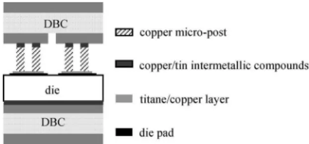
Fig. 1. Schematic of the proposed die interconnection using micro-posts. TABLE I
BONDINGMATERIALFAMILIESWITHTHEIRBONDING ANDREMELTING
TEMPERATURES[10]
II. MICROPOSTSINTERCONNECTIONOVERVIEW
The proposed interconnection is based on copper microposts that are electroplated on the topside of the die (see Fig. 1). The microposts have typically a square section in the range of 100 µm × 100 µm, up to 300 µm × 300 µm (to keep a suffi-cient density) and a height in the range of 100 µm. The distance between two microposts is fixed to 300 µm in the first step. Section dimension and postinterdistance are values to be opti-mized. Reducing section and increasing postdensity impact fa-vorably the mechanical rigidity and the thermal performance so far but could degrade reliability perspectives. Copper presents a good tradeoff between sufficient electrical and thermal conduc-tivities, cost, availability, and manufacturability. The microposts are realized by electroplating. Other plating methods like evap-oration, sputtering, and electroless do not allow in achieving affordably thicknesses close to 100 µm with large growth rate. Moreover, this plating method requires few equipments, and is thus low cost.
The die with its copper microposts is attached to the top direct-bonding copper (DBC) substrate by copper (Cu)/tin (Sn) transient liquid phase (TLP) bonding step (see Fig. 1). The TLP bonding step uses a low-melting temperature metal (tin, in-dium, . . .) to bond two high melting temperature metals (nickel, copper, silver, gold, . . .) together [10]. During the TLP bond-ing that necessitates quite a high temperature, pressure, and time-sensitive procedure, the diffusion of the low-melting tem-perature metal in the high-melting temtem-perature metals induces a formation of intermetallic compounds. The presence of in-termetallic compounds permits to have a joint with a remelt-ing temperature more important than its bondremelt-ing temperature. Table I lists some TLP bonding material families with their bonding and remelting temperatures. The DBC substrate was selected for compatibility with the copper microposts. Other combinations may be considered but have not been tested so far.
The main interests of the proposed microposts interconnec-tion are the eliminainterconnec-tion of a solder layer between the die pads and the interconnection on the one hand. On the other hand, the Cu/Sn TLP bonding allows in achieving joints with a high remelting temperature above 300◦C, and so is a solution
com-patible so far with high temperature packaging [10]. The other advantages are the following. The small sizes of the microposts permit to create a matrix of contacts on a usual power die. It decreases the values of parasitic inductance and electrical resistance. From a thermal point of view, the microposts inter-connection offers a thermal access on the topside of the die. The proportion of heat flux removal through this top connexion has not been yet measured but finite-element method simulations indicate a ratio of 20%–30% of the total heat flow (static oper-ating conditions with COMSOL). It is then safe to consider a positive impact on the junction operating temperature of the die. The possibility to introduce a dielectric fluid and/or gel between the microposts will allow improving the heat flux dissipation from the topside of the die.
III. MANUFACTURING ANDELECTRICALCHARACTERIZATION OF THEMICROPOSTSINTERCONNECTION
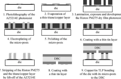
The different manufacturing steps to realize the microposts interconnection on a chip are presented in Fig. 2. Before the electroplating of the microposts, the die pads must be covered with a thin titane (Ti)/copper (Cu) layer (20/100 nm, respec-tively) if the pads are ready for wire bonding or bump. Properly prepared pads for copper electroplating would suppress this pri-mary preparation of the die. Titane is used as an adhesion layer and copper is employed as a conductive layer for the electro-plating step. Before the deposition of the Ti/Cu layer, a pho-tolithography step isolates the die pads (photoresist thickness close to 2 µm). This photoresist will permit to remove the Ti/Cu layer around the die pads by lift-off after the electroplating of the microposts, and so to avoid the short circuit between the die pads.
A second masking step is performed prior to the electrolytic growth of the microposts using a dry film photoresist (Riston PM275 dry film photoresist [11]) mainly seen in the electronics industry to realize printed circuit boards. The dry film pho-toresist is composed of a phopho-toresist sandwiched between a polyethylene protective foil and a polyester support. It offers some benefits such as a simple process, a remarkable robust-ness to the acid bath, a decrease in the edge beads on the sub-strate, and a low cost. The dry film photoresist has a thickness of 75 µm and a nominal resolution of 50 µm. The process to realize the pattern in one layer of the Riston PM275 is the fol-lowing. The die is heated at 70◦C for 1 min. This heating step
allows improving the dry film photoresist adhesion on the die. The polyethylene foil is removed. The photoresist is deposited by lamination on the die (100◦C and 0.3 MPa pressure). It is
then exposed to an UV source with an intensity between 12 and 15 mW/cm2, and a wave length of 385 nm, respectively.
The exposure time is comprised between 5 and 7 s, respectively. After lamination and exposure, the polyester support is peeled away. Finally, the photoresist is developed with a spray system
Fig. 2. Manufacturing process of the proposed interconnection.
in a sodium carbonate solution at 1% (5 g of sodium carbonate diluted in 500 mL of water) during 1 min and 30 s and with a processing temperature of 30◦C. The experimental electrolytic
cell has horizontal electrodes. This configuration allows ob-taining homogeneous microposts. The electrolytic bath is com-posed of pentahydrate copper sulphate (220 g/L), sulphuric acid (32 mL/L), hydrochloric acid (0.2 mL/L), and brightener and leveler additives (2 mL/L of Rubin T200-A, 8 mL/L of Rubin T200-G and 2 mL/L of Rubin T200-E). Electroplating of the microposts is performed at ambient temperature with a typical current density of 10 mA/cm2. The experimental growth rate
of the microposts is linear and close to 11 µm/h, for a current density of 10 mA/cm2. The minimal deposit time has been set
to 7 h. This deposit time achieves a microposts growth with a height larger than the thickness of the Riston PM275, and so al-lows then for a polishing and/or grinding step of the microposts in order to obtain a plane surface and ensure a good electri-cal and thermal contact between the microposts and the DBC substrate. A mechanical polishing is realized thanks to a cloth polishing disk and a diamond liquid with grains of 9 µm down to 1 µm in the laboratory-scale experiment. Thinner grains are available to improve further the state of surface. Fig. 3 shows the microposts for a deposit time of 8 h before and after the pol-ishing step. The height of the microposts is, respectively, 96 and 62 µm before and after the polishing step. This step is essential to obtain a fixed final thickness of the die in case of multi-dice modules with dice of different initial thickness. A quite good tolerance is achievable with a grinding/polishing step (namely in the 100 nm range and better). This avoids the use of inter-calars that multiply the interfaces if not increase the number of solder interfaces [12].
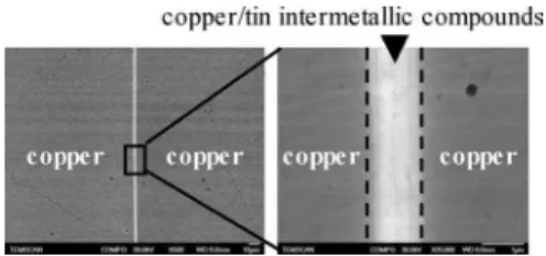
A diode die with its polished microposts is attached by Cu/Sn TLP bonding to the DBC substrate. A thin tin layer (thickness less than 1 µm) is deposited on the microposts and the DBC sub-strate. The tin thickness and bonding temperature are deduced from the Cu/Sn phase diagram in order to obtain a Cu-rich/Sn
Fig. 3. SEM images of the microposts for a deposit time of 8 h before (a) and after (b) the grinding/polishing step.
Fig. 4. Diode interconnected concurrently to top and bottom DBC.
joint. Fig. 4 presents a 3.5 kV-100 A diode with microposts on anode side and bonded concurrently to a top and bottom DBC through Cu/Sn TLP proposal. A tin thickness of 0,5 µm, a pres-sure of 10 MPa and a temperature of 300◦C during 7 min have
been considered. A SEM image of the Cu/Sn joint between a microposts and a DBC is shown in Fig. 5. As a demonstration of a 3.5 kV-100 A diode integrity after interconnection process, the direct electrical characteristic is pictured in Fig. 6. This characteristic is identical to the manufacturer datasheet [13].
IV. DISCUSSION
The previous sections cover the details of a first experiment of a proposed interconnection technique to avoid wire bond and solder. So far only the feasibility of the technique has been demonstrated since many issues are under investigation: influence of micropost dimensions with regard to die pad di-mension and positioning, parameters of electroplating growth
1670 IEEE TRANSACTIONS ON POWER ELECTRONICS, VOL. 25, NO. 7, JULY 2010
Fig. 5. SEM image of a Cu/Sn joint between a microposts and a DBC.
Fig. 6. Direct electrical characteristic of a 3.5 kV-100 A diode with the mi-croposts interconnection.
TABLE II
COMPARISON OFACTUALPACKAGINGTECHNOLOGIESWITH THEMICROPOSTS
INTERCONNECTION
rate, tolerance of grinding/polishing step, optimal parameters of Cu/Sn TLP bonding, thermal performance measurement of assembly, intrinsic reliability analysis, interconnection parasitic components measurement and reliability of a multidice assem-bly. Probably the optimal parameters of TLP-bonding depend on the industrial setup. However, the copper intermetallic inter-face is under analysis to relate the shear force capability to the metallurgical composition. The dimensions of the microposts have a significant influence on the thermal performance of the assembly and the parasitic components. The latter components
make sense with respect to commutation what implies to realize a two-dice assembly (a diode and a MOSFET, for example). The accuracy of the grinding/polishing step is then of primary im-portance. So, a complete experiment plan is required and under development. Table II presents a comparison of actual packag-ing technologies to situate the micro-posts interconnection.
V. CONCLUSION
This letter has presented an alternative interconnection solu-tion for power semiconductor dice that wishes to be compati-ble with 3-D integration of power modules. The different steps (electroplating and assembly by Cu/Sn TLP bonding) have been described. A first demonstrator on diode dice proves the feasi-bility of the proposal as the electrical characterization shows that the diode has kept its integrity and a satisfying electrical connection is obtained. Near future work focuses the produc-tion of a switching-cell (diode/MOSFET) for electrical tran-sient characterizations and thermomechanical analysis. More-over, electromagnetic and thermal simulations of the microposts interconnection will then be validated.
REFERENCES
[1] K. Xing, F.-C. Lee, and D. Borojevic, “Extraction of parasitics within wire bond IGBT modules,” in Proc. IEEE Appl. Power Electron. Conf. Expo., Feb. 1998, pp. 497–503.
[2] M. Ciappa, “Selected failure mechanisms of modern power modules,”
Microelectron. Rel., vol. 42, no. 4, pp. 653–667, Apr. 2002.
[3] J.-N. Catala, J.-G. Bai, X. Liu, S. Wen, and G.-Q. Lu, “Three dimensional packaging for power semiconductor devices and modules,” IEEE Trans.
Adv. Packag., vol. 28, no. 3, pp. 404–412, Aug. 2005.
[4] X. He, X. Zeng, X. Yang, and Z. Wang, “A hybrid integrated power electronic module based on pressure contact technology,” in Proc. IEEE
Power Electron. Spec. Conf., Jun. 2006, pp. 1–5.
[5] E. Vagnon, J.-C. Cr´ebier, Y. Avenas, and P.-O. Jeannin, “Study and realiza-tion of a low force 3D press-pack power module,” IEEE Power Electron.
Spec. Conf., Jul. 2008, pp. 1048–1053.
[6] J.-G. Bai, J.-N. Catala, and G.-Q. Lu, “Comparative thermal and ther-momechanical analyses of solder bump and direct solder bonded power device packages having double sided cooling capability,” in Proc. IEEE
Appl. Power Electron. Conf. Expo., Feb. 2004, vol. 1, pp. 1240–1246. [7] L.-H. Zhang, X. Yang, F. Wang, and Z.-A. Wang, “Pressure contact
pack-aging for hybrid electric vehicle drive,” in Proc. IEEE Power Electron.
Spec. Conf., Jun. 2007, pp. 2228–2233.
[8] M. Mermet-Guyennet, “New structure of power integrated module,” in
Proc. Int. Conf. Integr. Power Syst., Jun. 2006, pp. 133–138.
[9] U. Scheuermann and F. Ebersberger, “Packaging of large area power chips—Extending the limits of standard module technology,” [Online]. Available: http://www.semikron.com
[10] W. Welch, J. Chae, and K. Najafi, “Transfer of metal MEMS packages using a wafer-level solder transfer technique,” IEEE Trans. Adv. Packag., vol. 28, no. 4, pp. 643–649, Nov. 2005.
[11] Dupont. (2006). “Datasheet Dupont Platemaster PM200,” [Online]. Avail-able: http://www2.dupont.com.
[12] Z. Liang, J.-D. V. Wyk, F.-C. Lee, D. Borojevic, E.-P. Scott, Z. Chen, and Y. Pang, “Integrated packaging of a 1 kW switching module using a novel planar integration technology,” IEEE Trans. Power Electron., vol. 19, no. 1, pp. 242–250, Jan. 2004.
[13] “Datasheet of SIDC185D350A6 diode,” Infineon, [Online]. Available: http://www.infineon.com.
[14] R. Fillion, E. Delgado, P. McConnelee, and R. Beaupre, “A high per-formance polymer thin film power electronics packaging technology,” in