HAL Id: hal-01072378
https://hal.archives-ouvertes.fr/hal-01072378
Submitted on 8 Oct 2014
HAL is a multi-disciplinary open access L’archive ouverte pluridisciplinaire HAL, est
Engineered inorganic core/shell nanoparticles
Patrice Mélinon, Sylvie Begin-Colin, Jean-Luc Duvail, Fabienne Gauffre,
Nathalie Herlin-Boime, Gilles Ledoux, Jérôme Plain, Peter Reiss, Fabien Silly,
Bénédicte Warot-Fonrose
To cite this version:
Patrice Mélinon, Sylvie Begin-Colin, Jean-Luc Duvail, Fabienne Gauffre, Nathalie Herlin-Boime, et al.. Engineered inorganic core/shell nanoparticles. Physics Reports, Elsevier, 2014, 543 (3), pp.163 -197. �10.1016/j.physrep.2014.05.003�. �hal-01072378�
Engineered inorganic core/shell nanoparticles
Patrice M´elinon
Institut Lumi`ere mati`ere Universit´e Claude Bernard Lyon 1 et CNRS et OMNT Domaine Scientifique de la Doua, Bˆatiment L´eon Brillouin 43 Boulevard du 11
Novembre 1918 F 69622 Villeurbanne, France
Sylvie Begin-Colin
IPCMS et OMNT 23 rue du Loess BP 43 67034 STRASBOURG Cedex 2 France
Jean Luc Duvail
IMN -UMR6502 et OMNT Campus Sciences : 2 rue de la Houssinire, BP32229, 44322 Nantes cedx3, France
Fabienne Gauffre
SPM et OMNT : Institut des sciences chimiques de Rennes - UMR 6226 263 Avenue du General Leclerc CS 74205 35042 RENNES Cedex, France
Nathalie Herlin Boime
, IRAMIS-NIMBE, Laboratoire Francis Perrin (CEA CNRS URA 2453) et OMNT, Bat 522, CEA Saclay, 91919 Gif/Yvette Cedex France
Gilles Ledoux
Institut Lumi`ere mati`ere Universit´e Claude Bernard Lyon 1 et CNRS et OMNT Domaine Scientifique de la Doua, Bˆatiment Alfred Kastler 43 Boulevard du 11 Novembre
1918 F 69622 Villeurbanne, France
J´erˆome Plain
Universit de technologie de Troyes LNIOICD , CNRS et OMNT 12 rue Marie Curie -CS 42060 - 10004 Troyes cedex, France
Peter Reiss
CEA Grenoble, INAC-SPrAM,UMR 5819 CEA-CNRS-UJF et OMNT, Grenoble cedex 9, France
Fabien Silly
B´en´edicte Warot-Fonrose
CEMES-CNRS, Universit´e de Toulouse et OMNT 29 rue Jeanne Marvig F 31055 Toulouse, France
Abstract
It has been for a long time recognized that nanoparticles are of great scientific interest as they are effectively a bridge between bulk materials and atomic structures. At first, size effects occurring in single elements have been studied. More recently, progress in chemical and physical synthesis routes permitted the preparation of more complex structures. Such structures take advantages of new adjustable parameters including stoichiometry, chemical ordering, shape and segregation opening new fields with tailored materials for biology, mechanics, optics magnetism, chemistry catalysis, solar cells and microelectronics. Among them, core/shell structures are a particular class of nanoparticles made with an inorganic core and one or several inorganic shell layer(s). In earlier work, the shell was merely used as a protective coating for the core. More recently, it has been shown that it is possible to tune the physical properties in a larger range than that of each material taken sep-arately. The goal of the present review is to discuss the basic properties of the different types of core/shell nanoparticles including a large variety of het-erostructures. We restrict ourselves on all inorganic (on inorganic/inorganic) core/shell structures. In the light of recent developments, the applications of inorganic core/shell particles are found in many fields including biology,
of the properties, general concepts based on solid state physics are consid-ered for material selection and for identifying criteria linking the core/shell structure and its resulting properties. Chemical and physical routes for the synthesis and specific methods for the study of core/shell nanoparticle are briefly discussed.
Keywords: nanoparticle, core shell, synthesis, plasmonics
1. Introduction
Nanoparticles Nps can be considered as a new state of matter building a bridge between bulk materials and atomic or molecular structures. A bulk material should have constant physical properties regardless of its size, how-ever at the nano-scale size-dependent properties are often observed. It is generally admitted that size effects occur when the physical characteristic length under consideration is of the same order of magnitude as the size. Furthermore, at the nanoscale quantum effects illustrated by rehybridization or charge transfer affect the properties of the elements leading to ”novel prop-erties”. At first, size effects occurring in single elements have been studied. More recently, progress in chemical and physical synthesis routes permitted the preparation of binary and more complex structures. Such structures take advantages of new adjustable parameters including stoichiometry, chemical ordering, shape and segregation. In this regard, such complex nanostruc-tures have also become of interest as they offer additional degrees of freedom opening new fields with tailored materials for biology [1], mechanics [2], op-tics [3, 4], magnetism [5], chemistry [6] catalysis (including photocatalysis [7]), solar cells [8] and microelectronics. Among them, core/shell structures
[9] are a particular class of NPs consisting of an inorganic core and one or several inorganic shell layer(s). In earlier works, the shell was merely used as a protective coating for the core. In this case the shell acts as a barrier against impinging atoms or ions making the nanocrystals less sensitive to en-vironmental changes [10]. Moreover the shell contributes to the passivation of the core surface suppressing surface electronic trap states. The former fea-ture is well evidenced in electrochemistry where electrodes remain effective for a long time in fuel cells and batteries [11]. The latter is illustrated by the enhanced fluorescence quantum yield of semiconducting nanocrystals upon overgrowth with an appropriate shell. In the field of catalysis, core/shell structures enable atom economy of precious catalyst metals by using them only in the shell while applying an inert core material as support. Core/shell structures are also used in solid state reaction metallurgy where the particle growth can be done in a ’size focusing’ regime allowing strategies for ma-nipulating precipitates narrow size distributions [12]. More recently, by the appropriate choice of the core and shell materials, it has been shown that it is possible to tune the properties (optical, reactivity ,magnetic /ldots) in a spectral window larger than the window of each material taken separately [13]. This review mainly focuses on systems with specific properties arising from the core/shell structure. These properties are due to the polarization, rehybridization or charge transfer induced by the difference between both constituents. The interface between the two elements is of prime impor-tance. The goal of the present review is to discuss the basic properties of the different types of core/shell NPs including a large variety of heterostructures:
ductor [14] and insulator/insulator. We restrict ourselves mainly on inorganic core/shell structures, possibly stabilized by organic ligands in the colloidal state. Core/shell structures have found applications in many fields including biology, chemistry, physics and engineering. Among numerous review papers [14, 9, 3] dedicated to core/shell structures, we focus on a representative overview of their physical aspects. In addition, we discuss general consid-erations for the choice of materials starting from a solid state physics point of view, considering the core/shell structure as ultimate segregated system where the shell perfectly wets the core. The resulting criteria for core/shell structure predictions and related properties, especially the coupling between NPs and surrounding medium through plasmonic properties, are aimed to be of practical use for the interested reader. Chemical and physical routes for the synthesis and specific methods for the study of core/shell NPs are also briefly discussed.
2. Synthesis of core/shell structures
2.1. Chemical route
There is a large panel of chemical synthesis methods for colloidal inorganic NPs. The chemical synthesis of core/shell NPs can be roughly divided into two main strategies: 1) Synthesis of the core NPs, followed by the shell growth on their surface. This method is by far the most widely applied procedure. 2) cation exchange
2.1.1. Synthesis of the core nanoparticles
In the case of oxide core/shell NPs, the main methods to synthesize the core comprise 1) synthesis in aqueous systems (co-precipitation, sol-gel . . . )
by precipitation of reagents and 2) solvothermal methods based on the de-composition of metal precursors in presence of surfactants. This decomposi-tion may be induced by different energy sources (thermal, microwave, light . . . ). Then the core is coated either by an inorganic ceramic or metallic coating and silica are among the most reported and used coating. For the generation of silica coatings on the surface of metal oxide and magnetic NPs, the St¨ober method and sol-gel [11] processes are the most common choices. The St¨ober method relies on the addition of tetraethoxysilane (TEOS) to NPs dispersed in aqueous phase in presence of an alcohol (e.g. ethanol) and ammonium hydroxide. The thickness of the coating can generally be tuned by varying the concentration of ammonium hydroxide and the ratio of TEOS to H2O. In microemulsion synthesis [15, 16] micelles (e.g. St¨ober process) or
inverse micelles are used to confine and control the silica coating on core NPs. While a controlled silica shell thickness can be obtained, a drawback of this method is the difficult separation of the core/shell NPs from the large amount of surfactants associated with the microemulsion system. Aerosol pyrolysis has also been used for silica coating, but the structure of the composite NPs is commonly of ”mosaic type”, such as hollow silica spheres with iron oxide shells [17, 18]. To overcome shortcomings related to many aqueous synthesis processes, which concern colloidal stability, (i.e. NPs aggregation state) and final particle size, the synthesis of core/shell particles in organic solvents us-ing solvothermal methods is widely developed. It affords further improved control over size and shape and thus higher modulation in core/shell struc-tures and in the resulting properties [19, 20]. Solvothermal methods lead to
particles in organic solvents.
In the case of semiconductor/semiconductor or (oxyde or metal) mag-netic/magnetic core/shell nanocrystals, shell growth is mainly carried out in the same high boiling point organic solvents as for the core synthesis follow-ing a seed-mediated growth approach [14, 21, 22]. After the core synthesis, the shell precursors are generally slowly added or fully added with a con-trolled amount in order to avoid homogeneous nucleation of the shell mate-rial. Using such a seed mediated growth approach several type of oxide/oxide (MxF e3−xO4/F exM3−x′ O4 with M or M’=Fe, Zn, Ni, Mn) or metal/oxide
(often F e3− XO4/Au)or metal/metal (M/M’ with M or M’ = Au, Ag, Fe,
Co, FePt, CoPt . . . )and the inverted structures have been synthesized. The thickness of the shell is mainly controlled by the introduced amount of shell precursor but the size of core may influence the growth of the shell leading either to core-shell or dumbell or flower structures [23, 24, 25].
A variant, leading to a very good control of the shell thickness, is the so-called SILAR (selective ion layer adsorption and reaction) method. Here, a precisely calculated amount of the cation and anion precursors are added in an alternating manner, so that at each step half of a monolayer is formed. The most well known system in this context is CdSe/CdS [26, 27], for which a very narrow size distribution could be obtained even for very thick shells (> 10 monolayers). In the case of semiconductor nanocrystals obtained by aqueous synthesis, shell growth is mainly performed by the decomposition of the thiol ligands like mercaptopropionic acid, thioglycolyc acid or glutathione [28]. This decomposition, leading to a metal sulfide shell, can be assisted by UV-irradiation. Typical examples are CdTe/CdS and ZnSe/ZnS [29, 30].
Adding the shell precursors during the core nanoparticle synthesis can formally be considered as a single-step variant of the described two-step syn-thesis. The idea behind this approach is to promote the sequential growth of the core and shell materials by carefully adjusting the reaction condi-tions. In particular, the core and shell precursors have to be chosen in a way that they exhibit a difference in reactivity. Nonetheless this method favors the formation of graded or alloy structures rather than of systems with an abrupt core/shell interface. Examples using this single-step approach com-prise highly luminescent InP/ZnS [31] and Cd1−xZnxSe1−ySy nanocrystals
[32] or Co NPs coated with a Au shell achieved by heating the Co particles in 1,2-dichlorobenzene, under reflux, with [(C8H17)4N ]+[AuCl4] containing
tri-octylphosphine (TOP) as a stabilizer and the core-shell structure was formed by a process of redox transmetallation between Co0 and Au3+ [33].
2.1.2. Cation exchange
In contrast to method 1), the shell material is generated at the expense of the core, by replacing the cations in the ionic crystal lattice. As a con-sequence, the overall nanoparticle size and shape are essentially maintained thanks to the anion sublattice, while the effective core size shrinks. In con-trast to bulk materials, the exchange kinetics are much faster in the case of nanocrystals, making it possible for many reactions to take place even at room temperature [34]. The cation exchange reaction is driven by a large excess of the incoming cation and/or the preferential solvation of the outgo-ing cation. Formation of a more stable crystal lattice can be an additional
fore difficulties for the direct shell growth. Typical examples are PbS/CdS and PbSe/CdSe core/shell nanocrystals [34, 35]. Furthermore, complex het-erostructures can be maintained during several subsequent cation exchange reactions, as for example illustrated by the transformation of a CdSe/CdS via Cu2Se/Cu2S to ZnSe/ZnS spherical core / elongated shell (dot in rod) structure [36]. On the other hand,better mechanistic understanding is still needed to enlarge this approach to other materials families. However, the observed mild reaction conditions, fast reaction times and the possibility to generate metastable heterostructures already demonstrate the potential of cation exchange as a powerful tool in the synthesis of novel core/shell sys-tems.
2.2. Physical route
2.2.1. Solvent-free fabrication of core/shell nanoparticles
In contrast to the numerous processes developed in the liquid phase, com-parably small number of solvent-free methods have been investigated to en-gineer such nanoarchitectures.
Chemical vapor deposition (CVD) is a well known technique to grow not only epitaxial semiconductor core/shell structures but also core/multishell nanoarchitectures. For example Lauhon et al. used CVD to grow core/multishell nanowire heterostructures [37]. These authors used a gold particle as a catalyst to grow a semiconducting nanowire using the appropriate gaseous reactant, Figure 1a,b. Then by subsequently introducing different reac-tants and/or dopants and tuning the experimental conditions to favour ho-mogeneous vapour-phase deposition on the nanowire surface by introduc-ing different reactants and/or dopants, the authors succeeded in producintroduc-ing
core/multishell wires, Figure 1c,d. Si-Ge and Si-Ge-Si core/shell nanowires created using this method are presented in Figure 1e,f.
While CVD is a clean method well suited to the growth of semiconductor core/shell materials [37, 39], different methods have to be developed for other systems such as metals. Habas et al. have shown that metal nanocrystals can be used as seeds for growing a metal crystalline shell [40]. Although the growth of the shell was done in the liquid phase, the concept can also be used in vacuum without any solvent. Various differently-shaped nanocrystals and NPs have been grown in vacuum after deposition of metal atoms on metal, semiconducting or insulating substrate surface. The subsequent diffusion of atoms of other species on top of the nanocrystal is expected to lead to the formation of core/shell structures.
Carbon cages can also be engineered in vacuum after deposition of metal atoms onto amorphous carbon thin films at elevated temperature. Transmis-sion electron microscopy reveals that in the case of nickel, the metal atoms form a core and then the carbon atoms of the substrate diffuse on the Ni core to form a multi-layer graphene shell, Figure 1 [38]. Interestingly ex-perimental data show that the graphene layers are growing inwards at the nickel-graphite interface. Carbon shells have also been engineered when Ni particles were heated in close proximity of C60 molecules [41].
The fabrication of core metal/shell structures in vacuum appears to be more problematic. The main drawback of depositing metal directly onto supported particles or nanocrystals is the shadow effect, i.e the side of the particle facing the evaporator is coated but it is usually not the case of
Figure 1: (left panel) Scheme of CVD growth of core/shell nanowires. (a) A gas, the reactants in red, reacts with the surface of a gold nanocluster, the catalyst. This leads to the directed growth of a nanowire (b). (c) When conditions are altered, the the reactant decomposes on the nanowire surface, leading to the formation of a uniform shell (blue). (d) Subsequent modulation of reactants leads to the growth of multiple shells . (e) Inset: TEM image of the Si-Ge core/shell nanowire. Nanowire cross-section indicates a 21 nm diameter Si core (blue circles), 10 nm Ge shell (red circles) and < 1 nm interface. (f) Si-Ge-Si core/shell nanowire cross-section shows a 20 nm diameter silicon core, a germanium inner shell (thickness, 30 nm), and p-type silicon outer shell (4 nm). Silicon is represented y blue circles and germanium is represented by red circles [37]. (right panel) Ni particle encapsulated by a graphite shell [38].
spheres on glass was only covering half of the spheres forming a half-shell [42]. The silica spheres can also be coated with a half-shell Ti/W film using the same process. Subsequent deposition of gold on the particles followed by an annealing at 700◦C leads to the dewetting of the gold film and the
formation of gold microcrystals on the surface of the spheres [43].
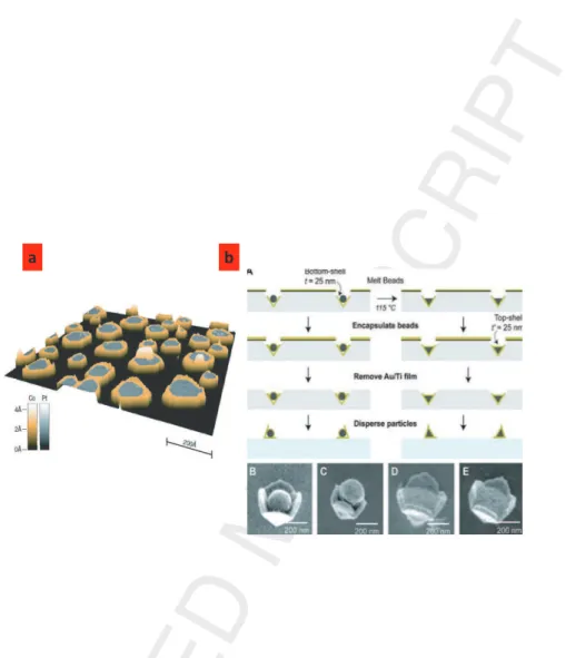
Sweeney et al. developed an elegant strategy to circumvent the shadow effect occurring during metal coating [44]. They fabricated bottom pyrami-dal shell using sequentially phase-shifting photolithography, etching, e-beam, and lift-off. First they made cavities in Au-Ti-coated Si(100) substrate. The cavities were then coated with a gold layer (25 nm thick). Silica (SiO2) or
polystyrene (PS) particles were then deposited in the cavities. The particles could be molten or not at high temperature to create different structures. Then a 25 nm Au layer was deposited using e-beam on top of the particle to complete the formation of the core/shell particles (see Figure 2). The sub-strate was then etched in order to release the core/shell particles. The whole sequence is illustrated in Figure 2 along with scanning electron microscopy images on these core/shell structures.
An alternative method for engineering metal core/shell structures con-sists in the subsequent deposition of metal atoms on surfaces. For example Rusponi et al. [45] have grown hexagonal Pt islands on a metal substrate in vacuum after deposition of 0.2 monolayer of Pt at 130 K followed by an-nealing at 760 K. The cobalt island outline was achieved after subsequent deposition of 0.2 monolayers of Co at 220 K, see Figure 2 a. 2D Pt par-ticles surrounded with Co rim were thus created but not yet supported 3D
Figure 2: a (left panel) Fabrication of core/shell particles. (A) Assembly of PS or SiO2
beads into pyramidal bottom shells, encapsulated with top shells, and then released to form pyramidal core/shell particles. (B, C) SEM images of Au-PS-Au particles with separated bottom and top shells because of swelling by the PS beads under e-beam deposition. (D, E) SEM images of Au-PSmelt-Au particles with flat dielectric surfaces covered by a top
shell [44]. b (right panel) 3D STM image of Pt islands (gray) surrounded by a single Co atom large crown [45].
Figure 3: (a) Method to fabricate Au@Pd core/shell NPs on Fe304surface. (b) Scheme of
Pt nanocrystals encapsulated with a FeO(111) layer [47].
a Co layer.
Davies et al. improved this method to grow core/shell particle on oxide surfaces [46]. They sequentially deposited gold and palladium onto a γ-Fe2O3(0001) substrate in ultra high vacuum by metal vapor deposition. The
two metals form distinct Au and and Pd particles on the oxide surface. Then the authors claimed that annealing this system at 573 K for 1 minute induces the diffusion of the Pd atoms on the Au particles and then leads to the formation of Au@Pd core/shell particles of few nanometer size. This method
Metal nanocrystals or nanoparticle encapsulated within an oxide thin film can also be fabricated after depositing metal on an oxide substrate followed by annealing at high temperature. Pt nanocrystals encapsulated within an FeO(111) monolayer have been created after deposition of Pt on Fe3O4(111)
followed by annealing at 850 K, Figure 3b [47]. In a similar way Pd nanocrys-tals grown on SrTiO3(100) surface are encapsulated within a TiO(111)
mono-layer after annealing at 900 K [48].
2.2.2. Gas phase synthesis
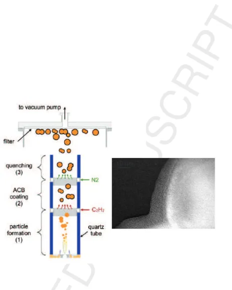
In the family of physical methods for the synthesis of NPs, gas phase synthesis methods are interesting because they offer a continuous way of NPs production and are therefore easily scalable. For example the Flame Spray Pyrolysis is developed at industrial scale. In this method, NPs are synthesized in a combustion flame in a gaseous flow and are collected in a filter placed downstream. Such methods have been implemented and are able to produce core/shell NPs in a simple way, the core is classically synthesized in the first reaction zone while the shell is added in a second reaction zone as shown in Figure 4
In this example [49], oxide NPs of LiF eP O4 are synthesized by flame
pyrolysis and coated in an oven by decomposition of ethylen with a rate of 7g/hour. A limitation of this method is the production of oxide cores, it can be overcome by the laser pyrolysis method that recently demonstrated the synthesis of Si@C NPs as shown in Figure 4 [50]. In both cases, the NPs were synthesized as elements of Li Ion batteries able to work at high capacity with improved cyclability.
10 nm
Figure 4: (left panel) Schematic diagram of the experimental setup for the production of LiF eP O4@C, LiF eP O4 is produced by combustion and coated by carbon in a second
reaction zone. The particles are collected after leaving the reaction zone in a flow of neutral gas after the reference [49].(right panel) Si@C core/shell NPs synthesized by laser pyrolysis in a reactor composed of two successive laser-reactant interaction zone. The Si core is synthesized from laser decomposition of silane and coated in a second reaction zone by laser decomposition of ethylen.
2.2.3. Preformed clusters in the gas phase
Ligand-free clusters well defined both in size and composition are cur-rently produced in free phase by nucleation in a seeded beam. Among them, laser vaporization source is widely developed. A target is ablated by a pulsed Nd:YAG laser creating a plasma. The plasma is cooled by a continuous flow of a buffer gas (He, Ar) triggering the formation of nucleation embryos. The formation of the NPs is obtained by accretion of the plasma species during a subsequent adiabatic expansion ( 108 K/s cooling rate) [51]. The
expan-sion occurs when the mixture flows through a micrometer nozzle separating the nucleation chamber at high pressure from the deposition chamber at low pressure. The advantage of the deposition of clusters with low energy is that they survive on the substrate essentially without fragmentation, and with little deformation [52]. For binary structures, a target pellet is made by the sintering of a mixture of the two elements. Even though clusters are produced in a non steady state, free survival clusters are close to the equi-librium shape and governed by the segregation rule [53]. Another versatile method has been first proposed by Hoshino etal [54] who prepared N a@Co clusters. The clusters are produced in a dual-target dual-laser vaporization cluster source, which allows producing binary clusters. By tuning the delay time between the two laser pulses, and then the embryo formation, A/B and B/A core/shell structures can be prepared [55, 56]. Compared with other existing methods for the generation of core/shell NPs, this method can be applied to a wider variety of materials. However, the method is limited to a low quantity of matter.
3. Experimental methods for the characterization of core/shell nanopar-ticles
Different experimental techniques are especially adapted to the charac-terization of core-shell structure and its interface.
3.1. Transmission Electron Microscopy TEM
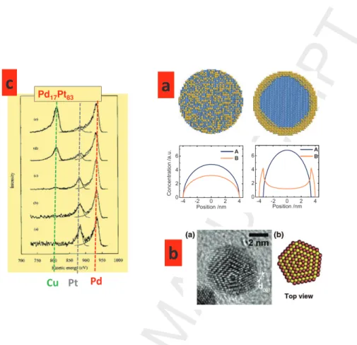
The transmission electron microscope allows not only for the observation of NPs but also the determination of quantitative information, like strain or chemical composition at the nanometer scale. This information is correlated with physical macroscopic measurements. The developments of quantita-tive electron microscopy have been possible through technical improvements among which are electron guns (working generally at 200kV or 300kV), elec-tron detectors and aberration correctors. For the latter, the image spheri-cal aberration correctors allow for improved spatial resolution and reduction of the interface delocalization [57] whereas the probe correctors reduce the probe size to measure chemical information at the atomic scale. This chemi-cal information can be extracted from three different detection systems cor-responding to different physical interactions. The high angle annular dark field microscopy (HAADF) gives a contrast depending approximately on the square of the atomic number Z2[58]. The exact interpretation of the HAADF
images requires however image simulation (figure 5a). The EEL (electron energy loss) and EDX (energy dispersive x-ray) spectroscopies correspond to the inelastic scattering of fast electrons with atoms in the nanoparticle. The fast electrons loose energy that is measured with an EEL spectrometer
ical composition [59] or oxidation degree, and also on optical or magnetic properties[60]. The material can be de-excited through x-ray emission that is measured by dedicated detectors [61]. EDX spectra provide information on the atom present in the NPs but the detailed electronic structure is not available due to the poor energy resolution and detection efficiency compared to EEL detectors.
The correction for the spherical aberration is mandatory to get the atomic resolution in both imaging and chemical analysis of inorganic nanoparticles. For soft matter, it is however necessary to correct also for the chromatic aberration that will limit the resolution at low voltages (below 80kV). The use of low voltage microscopy is more and more widespread to limit the effect of beam damages on the samples.
One aspect of the recent progress of electron microscopy concerns the study of the growth of particles inside the microscope. In a gaseous atmo-sphere, a dedicated pumping system is added around the objective lens or special sample holders allow for the gas injection inside a reactor [62]. The nanoparticle growth can also be observed in liquid cells where the reaction is initiated by an electron or a photon pulse [63]. More and more experiments are also proposed to study the samples ”in operando”, the aim is to follow the evolution of the sample under magnetic, optical or electrical solicitations. For the evolution of the magnetic configuration, many techniques in a TEM are available among which the electron holography has proven its efficiency on NPs [64].Study on NPs benefit from all the technical and experimental de-velopments in TEM for some years now, for structural and chemical aspects but also for the determination of local physical properties.
Pd17Pt83
Figure 5: some examples illustrating the observation of a core/shell structure. (a) ideal observation of a core/ shell structure by HAADF. (left) Cross-sectional view of a core/shell NP, (right) in a homogeneous alloy. The HHADF signal gives the concentration of the two materials, A and B, across the equator- ial plane of the particle (left) and (right), respectively (after the original figure of Xu and Wang [65]. Experiemental observations are well illustrated in this paper on figures 16,20, 21 and 22. (b) HRTEM image of a FePt particle displaying simultaneously a fivefold symmetry and L10 ordered domains with a schematic view of the corresponding chemically ordered decahedral structure, predicted by theoretical calculations. In this case the alloying is perfect (after the original figure of Tournus et al [66]. (c) Evolution of the LEIS signal during the 4
He+
1-keV ion bombardment of a P d65P t35sample after (a)=75 s, (b)=210 s,(c)=660 s, (d)=1335 s and
3.2. (cryo)-Tomography
The TEM techniques described in the previous part suffer from the trans-mission process that induces a projection of the whole sample on a single plane (figure 5b). The NPs are projected in a two-dimensional image and the three dimensional information is lost. Some techniques are available to investigate the 3rd dimension, such as electron tomography and atom probe
tomography. Several techniques have been developed in the field of electron tomography [68]. The classical one consists in the acquisition of series of images for various tilt angles and the reconstruction of the object through software calculations. The various angles are obtained by tilting the sample holder (monocrystals) or by looking for samples with different orientations (particles). The signal is usually recorded with an HAADF detector [69]. A second method is the discrete tomography method, that necessitates a small number of acquisition but requires the knowledge of the particle structure. This method is based on the fact that the HAADF signal recorded for each probe position is proportional to the atomic number and to the number of atoms in the column. Associated with statistical analysis and the acquisition along 3 different crystallographic axis, the 3D structure of silver particles in an aluminium matrix has been demonstrated on an aberration-corrected STEM [70]. Other reconstruction algorithms, as ”compressed sensing” are also studied with the idea of reconstructing a 3D image with few 2D images [71]. Using electron tomography, atomic columns can be imaged in plane but the depth of field cannot reach the atomic resolution along the optical axis.
The atom probe tomography is a combination of field ion microscopy, time-of-flight mass spectrometry and position sensitive detector. Historically,
most atom probes have used a voltage pulse to field evaporate atoms from the specimen. The samples are prepared as needles to enlarge the electric field at the tip and extract the atoms that are analyzed by the mass spectrometer. The study of conductive samples was spread to oxides or semi-conductors with the use of laser pulses focused on the tip. The 3D chemical image is re-constructed using dedicated software, in which various parameters have to be set. Complimentary microscopy analysis can be used, in particular HRTEM and STEM analysis to get these parameters.The screening distance of the electric field at the specimen surface determines the depth resolution. It is usually around 0.1 nm in conductive materials, the atomic resolution being achieved along that direction. Gold NPs embedded in a MgO matrix have been studied by atom probe tomography, making it possible to determine the composition of individual particles [72].
3.3. EXAFS, XPS
Among the many techniques linked to x-ray radiation available to analyze materials, absorption techniques and surface photoelectron spectroscopy will be detailed as they are the most commonly used. X-ray absorption spec-troscopy techniques (XAS) are used to study the structure of materials, by studying the local structure around selected atoms. XAS experiments are sensitive to chemical species and can be applied on materials without long-range order, making this technique unique among spectroscopy techniques. In x-ray absorption spectroscopy, the information comes from the transition of occupied levels to unoccupied valence orbitals. In XANES (X-ray Near
the vacant orbitals, electronic configuration and site symmetry of the ab-sorbing atom. In EXAFS (Extended X-ray Absorption Fine Structure), the oscillatory part of the absorption coefficient above a major absorption edge can indicate the number and species of neighbour atoms, their distance from the selected atom and the disorder (thermal or structural) of their positions. The interpretation of the oscillations requires the use of ab-initio calcula-tions. Commonly installed on synchrotron lines, the XAS experiments can be combined with a deposition chamber to follow the growth process of ma-terials.
X-ray Photoelectron Spectroscopy (XPS) probes the bonding energies of electrons by the analysis of the kinetic energy of the emitted electrons after an irradiation under monoenergetic x-ray photon beam (in the 200eV-4000eV range). If the incident energy is sufficient, a core electron will be ejected to the vacuum. Each chemical element is characterized by a spectrum with different peaks corresponding to different orbitals, from which the oxidation state of the material can be deduced [73]. The peak intensities depend on photoionization cross section and the comparison of the peak areas provides an quantitative analysis of the chemical composition. The position of the peaks can indicate some chemical shifts, keeping in mind that the energy reference is crucial in this kind of experiments [74]. The XPS experiments is limited to the analysis of information on the sample surface because of the short inelastic mean free path for electrons. This length is on the order of a few nanometers and depends on the material. In the case of core/shell nanoparticles, XPS using synchrotron radiation of variable energy enables to distinguish between core/shell and alloy nanoparticles even in the case of very
small dimensions (< 5nm) [75]. When lower energy photons are used to probe the surface, the spectroscopy is called UPS (UV photoelectron spectroscopy), the photon energy is in the 10-45 eV range. This spectroscopy is used to probe filled electron states in the valence band or adsorbed molecules on metal. By detecting photoelectrons at different emission angles, the energy of the electrons as a function of the momentum vector may be determined. This process is known as ”band mapping” and is a powerful probe of the electronic structure of crystalline materials. The distinction between UPS and XPS is becoming less and less well defined due to the continuous energy range available with synchrotron radiation.
3.4. Low energy ion scattering
Low Energy Ion Scattering technique (LEIS) is a powerful probe for seg-regation studies. Unfortunately, this method classified as destructive remains little known despite its high selectivity in depth profile and sensitivity [52, 67]. LEIS is a surface-sensitive technique that selectively probes the outermost atomic layer and is therefore well adapted to the study of surface segregation. A beam of monoenergetic (energy E0 about 1keV ) He+ ions of mass M1 is
focused on the surface of interest. Some of these ions are backscattered from the surface through an angle θ and their energy distribution is analyzed. The intensity of the LEIS signal is mainly assigned to the collisions involving the first atomic layer (figure 5c). The position of the elastic ion peak is given by the simple relationship assuming hard sphere model
where M2 is the mass of the surface atom involved in the collision. The
same equation is valid for a binary compound. Note that E gives through M2
measurement the nature of the atom. At the onset, the superposition of two signals (M2 and M
′
2masses) in the backscattering energy spectrum is related
to alloying, one signal being related to a pure shell. The intensity calibration is done with reference samples (single crystals with different orientations). Since a low sputtering is observed, a depth profile can be obtained as a function of time.
4. Core/shell nanoparticles: specific advantages arising from the heterostructure
4.1. A rapid survey
Core/shell structure refers to a multilayered particle which is the result of core and shell division where the core is totally surrounded by the shell (onion-like structure)(figure 6). This is a particular case of total segregation in an alloyed particle. Total segregation leads to two classes of multilay-ered particles Janus and core/shell type. The main difference between the core/shell particles and the Janus particles (dedicated to Janus in roman mythology, a two-faced god looking in the future and the past) is the mor-phological features of their components mutual arrangement, where there is only one of them on the surface of core/shell NPs. These Janus NPs have different properties (such as charge, polarity, optical or magnetic properties) at opposite sides while core/shell NPs have properties arising of those of the core or the shell. Their combination can also give rise to novel properties, not achievable with the individual materials alone. Core/shell NPs can be
Figure 6: Some examples illustrating different configurations in a binary system. The completely phase segregated has two forms: a core/shell (right) and a Janus form (left) after the original figure from Wanjala et al [76]
classified in two groups according to the role of the shell:
-shell as core protection
This is well illustrated in Co/X or Fe/X (X coinage metal) where the non reactive metal at the surface of the magnetic nanoparticle is a suitable pro-tecting tool [10]. The magnetic property is related to the core as long as no polarization effect or sizeable electron transfer is observed.
-”smart shell” with targeted properties
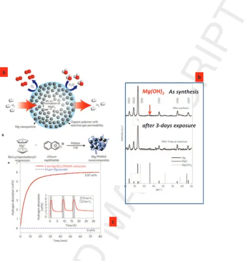
We only consider the case where the shell contributes to the passivation of the core surface suppressing surface trap states without noticeable alteration of the electronic properties. Jeon et al [77] reported the synthesis of metallic Mg nanocrystals embedded in a gas-barrier polymer matrix(PMMA) that en-ables both the storage of a high density of hydrogen and rapid kinetics with applications in fuel cells batteries (Figure 7). This core/shell structure illus-trates well the selective coating which protects the core from the oxidation and which is permeable to the hydrogen migration.
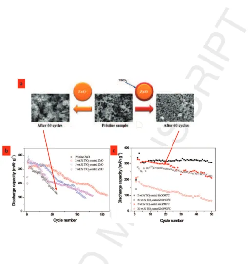
Likewise, Lee et al [11] studied ZnO/T iO2 NPs produced by the sol-gel
method for batteries. In this case, the T iO2 avoids the migration and the
dissolution of Zn in the electrolyte, T iO2 remaining a transparent barrier
for ion migration (T iO2 has high ionic conductivity and is very resistant
to corrosion). This is well illustrated by the low softening of the discharge capacities against cycle number (figure 8).
Figure 7: Mg NPs in a gas-barrier polymer matrix. (a) Schematic of Mg NPs encapsulated by a selectively gas-permeable polymer with a synthetic approach to formation of Mg NPs embedded in PMMA nanocomposites. (b) The diffraction pattern reveals pure Mg without alteration after an long time exposure (3 days at air). This illustrates the coating efficiency with a no sizeable (M g(OH)x) contribution (the expected diffraction peaks in oxides are
displayed).(c) enhancement in hydrogen absorption properties of M g@P M M A composites (absorption at 200oC and 35 bar of H
2) in comparison to bulk powder Mg. The maximum
of hydrogen absorption is reached after one hour, the value is close to the theoretical one (7.6%). The stability is also observed by the reversible absorption-desorption cycle (after the original work from Jeon et al [77])
Figure 8: Discharge capacities of pure ZnO pristine, 2, 5, and 7 wt % T iO2- coated ZnO
and (b) discharge capacities of 2 and 20 wt % T iO2-coated ZnO annealed at 500 and
900oC. At low temperature (< 500oC) T iO
2 is in anatase structure. Above 500oC a
transition towards rutile phase is observed and corresponds to an enhancement of the protection. At this stage a core/shell structure is expected. At high temperature 700oC
and above, a partial alloying with ZnT iO3and Zn2T iO4phases is reported especially in
Ti-rich compounds. This corresponds to a lower efficiency with the lack of the core/shell structure. The morphology of the ZnO@T iO2electrodes is also given after 60 cycles. The
dendritic forms observed in pure pristine exhibits the dissolution and recrystallization of zinc atoms during the electrochemical process (after the original work of Lee et al reference [11] .
Figure 9: Schematic representation showing the separation, fluorescence imaging and pho-tothermal destruction of cancer cells using magnetic@plasmonic NPs (from reference [82].
a strategy to protect their spontaneously oxidizable surfaces and provide a surface for chemical functionalization [78, 79]. The ability to combine the magnetic and optical properties of the composite material opened new perspectives for biomedical applications. To this aim, complex structures such as iron oxide/silica/Au NPs or star-shaped iron oxide/gold NPs were engineered, simultaneously enabling multiple functions such as MRI imaging, magnetic guiding and NIR photothermal therapy (figure 9) [79, 80, 81, 82, 83, 84].
4.2. Hollow structures
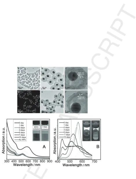
Among core/shell structures, hollow nanocrystals [85] offer applications in nanoelectronics, nano-optics, drug delivery systems, and as building blocks for lightweight materials. Even though the chemical route is the standard procedure for hollow structure synthesis [86, 87], a physical route based from the conversion of solid to hollow NPs known as the ”nanoscale Kirkendall effect” was successfully investigated [88]. The Kirkendall effect is the motion of a boundary layer between two elements that occurs as the consequence of the sizeable diffusion rates between the two elements at high temperature. Caruso et al [89] showed that the thickness of the hollow sphere as well its size and shape can be readily controlled during growth. A new class of core/shell NPs with the core lying in a hollow cavity opens an alternative way to tune the coupling between the optical features of both metal and non-metal counterparts. While solid Au/CdSe/CdS core/shell/shell NPs do not show any fluorescence, a fluorescence signal albeit with low quantum yield (0.8%) is observed for hollow core/-shell NPs after etching CdSe by dilute H2O2(Figure 10) [90]. The increased fluorescence of hollow NPs versus solid
ones presumably results from a decrease of the density of CdS surface trap states due to a mild oxidation by H2O2. Furthermore, a weakening of the
quenching effect induced by the Au core could contribute considering that the distances between Au cores and some parts of CdS increases due to the movement of the cores in the rattle structures after CdSe removal.
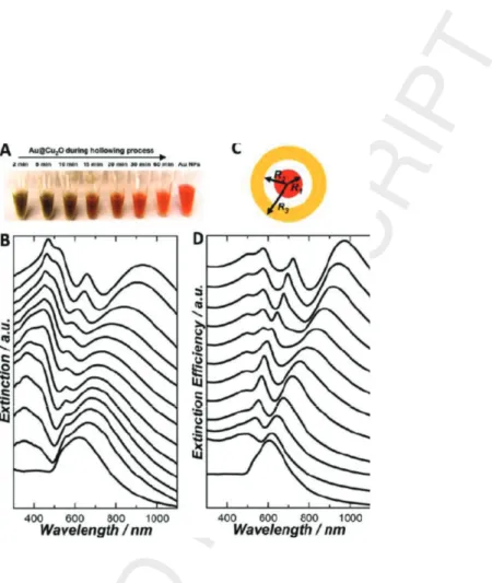
Another example of the tunability offered by hollow cavity between the core and the shell is given by Au/Cu2O NPs [91] (fig. 11). The engineering
geo-Figure 10: Transmission electron microscopy images of Au@CdS nanostructures after etching of CdSe by dilute H2O2for 7 days (A-C) and 15 days (D-F). The overall sizes are
44 nm. The fluorescence spectra of Au@CdSe@CdS hollow NPs are shown A) UV-vis and B) for different oxidation time (from the reference[90]).
metrical parameters, such as Cu2O shell thickness, size of the Au core, and
the spacing between the core and shell. Finally, selective ion diffusion can be used for the elaboration of novel core/shell structures, which do not contain obligatorily a cavity. An example is the transformation of ǫ-Co nanopar-ticles into Co/Co-P core/shell structures containing an amorphous cobalt phosphide shell [92]. This intermediate structure is obtained by inward P diffusion preceding the complete transformation of ǫ-Co into Co2P
nanopar-ticles through subsequent outward Co diffusion accompanied by Kirkendall hollowing.
4.3. Self focusing in solid state reactions
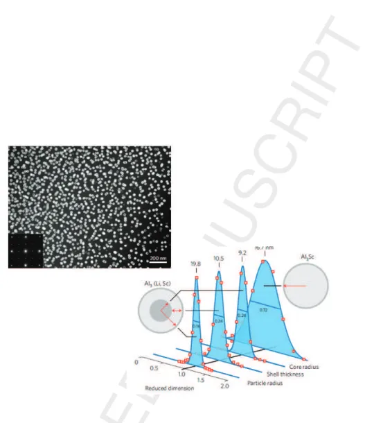
In classical nucleation theory, the radius (hence the surface/volume ratio) is of prime importance. The capability to change the surface energy through the net concentration of A (core) or B (shell) atoms at the surface offers a new degree of freedom. Then, core/shell structures can be used to monitor nucle-ation and growth with a self focusing effect (figure 12). Radmilovic et al [12] prepared the ternary compound Al-Sc-Li with a core of Al3(Sc; Li),
incorpo-rating both Sc and Li on the B-site sublattice of the L12A3B structure and a
Al3Li shell. They found a remarkably uniform distribution of core/shell
pre-cipitates with L12 structure (such binary compounds Al3X type intermetallic
phases crystallizes in the L12 structure) even though without size selection
(figure 12). However, the self focusing in the nucleation growth requires drastic conditions on temperature range, phase diagram, diffusion factor and solubility (trend to alloying) of each element in the final compound. The self focusing regime is reached when ∂2r
∂t2 < 0 ( ∂r∂t < 0 determines the critical
Figure 11: Optical tunability of Au@Cu2O NPs. (A) Photograph of colloidal suspensions
with an average Au@Cu2O outer radius of 130 nm obtained at different reaction times
during the symmetric hollowing of Cu2O shells. The right-most sample is bare Au colloids.
(B) Experimentally measured extinction spectra of colloidal suspensions of Au@Cu2O NPs
obtained at different reaction times: 2, 5, 10, 15, 20, 25, 30, 40, 50, 60, 75, and 90 min (from top to bottom). The bottom spectrum is corresponding to bare Au colloids. (C) Geometry of Au@Cu2O employed for Mie scattering theory calculations. (D) Calculated
extinction spectra of a Au@Cu2O with fixed R1 of 63 nm, fixed R3 of 130 nm, and varying
R2 of 64, 65, 66, 68, 70, 75, 80, 86, 93, 100, and 110 nm (from top to bottom). The bottom curve is the calculated spectrum of a spherical Au nanoparticle (63 nm in radius) (after the reference [91]).
Figure 12: Size distributions of core/shell AlLiSc NPs measured with dark field TEM showing an uniform distribution of core/shell precipitates with L12structure(see the weak
reflections of the L12superlattice in the Fourier transform (in insert). The strong
reflec-tions correspond to (100) crystal orientation. The size distribution is shown in the right part compared to the broad distribution of Al3Sc compound where no self focusing is
severe conditions limit the self-focusing regime, formation of a core/shell nanostructure is a method for in situ size selection during growth.
4.4. Beyond surface protection: application to catalysis
Now, let us consider the case where the shell modifies the electronic prop-erties. It has been shown that it is possible to tune the physical properties in a larger window than that of each constituent taken separately by the appropriate choice of the core and shell materials. This opens a new field of tailored nanomaterials with high selectivity and high sensitivity especially for catalysis or plasmonic applications.
4.4.1. Metal catalysts
Turkevich and Kim [93] introduced a very important concept of cataly-sis using two different metals such as Au and Pd in the same nanoparticle. Core/shell nanostructures are a convenient way to integrate multifunctional-ity into the electrocatalysts of metallic NPs. Catalysts are often expensive. At a first glance, in NPs of catalyst metal, the center atoms are burried and cannot take part in reactions. A core/shell particle can be constructed in a way that the catalyst atoms are located only on the outside (the shell re-gion), while the core can be constituted by a catalytically inactive low-cost material. This structure has the advantage in that all the catalyst atoms can take part in reactions. In this case, the core does not play a significant role excepted for the shell growth. This crude assumption holds for large shell thicknesses when the core atoms are totally embedded and located far away from the surface. In other words, the core atoms do not introduce a
pertur-large (typically few angstroms) as compared to the Thomas Fermi screening of the core atom into the shell medium. For applications, electrocatalysts need to be highly active and durable under harsh reactive environments. It is therefore advantageous to protect the catalyst with another element. Sekol
et al [94] synthesized Ag/Pd catalyst NPs supported on multi-walled
car-bon nanotubes for use in fuel cells. The new catalysts are highly active and alcohol-tolerant for oxygen reduction reactions (ORR) in alkaline media. For the smallest ones where the shell is very thin, the core atoms are partially exposed and can serve as catalytic active sites. Core/shell structures can be used to engineer materials with tailored properties, concerning polarization, delocalization, hybridization or massive electron transfer between core (shell) and shell (core). This is the key point for the enhancement of catalytic activ-ity [95]. Very recently, Qi et al [13] reported an enhanced catalytic activactiv-ity of core shell Au/CeO2NPs compared to Au−CeO2having a Janus form (Au
deposited onto CeO2). In addition, these authors found a remarkable
stabil-ity upon CO oxidation (figure 13). The key point is the interfacial bonding between the core and shell which can alter the electronic structure with an enhancement of the net activity and stability [96]. Note that both effects are antagonist since a good activity requires a thin protection film (shell) while a good stability requires a large capping. The ideal compromise is probably with one monolayer as suggested by Hwang et al [97]. However, this is a pure illusion since for uncomplete shell, the adatoms occupy preferentially either under coordinated or over coordinated sites at the surface.
A very promising application of the core/shell nanostructure is the con-cept of bifunctional systems where two reactions are monitored within the
same nanoparticle [98]. For example, Ni/Ru NPs have been demonstrated to act as a bifunctional system for the hydrolysis reaction of ammoniaborane and also for magnetic separation [99]. For fuel cell applications Chen et al [100] proposed a bifunctional catalyst where the core (oxides) material cat-alyzes an oxygen evolution reaction whereas the shell (nitrogen doped carbon fibers) material catalyzes an oxygen reduction reaction. This field of appli-cation is very promising, because in full rise for the realization of selective and efficient effects in catalysis science.
4.4.2. Oxides catalysts
In the context of environmental and energy shortage concerns, photocat-alyst efficient for air and water treatment by decomposition of organic pol-lutants and water splitting for hydrogen production are subjects of intense research activity. Due to its good chemical stability, weak toxicity and low cost, T iO2 is the most used oxide photocatalyst but several limitations must
be overcome. T iO2, as many photocatalyst, is active mainly under UV light,
leaving apart a large part of the solar spectrum. Therefore many studies are dealing with the engineering of the bandgap (stoichiometry, insertion of het-eroatoms . . . ) in order to shift the absorption towards the visible range. In the photocatalysis process, an electron-hole pair is created under excitation. Ideally, the electron and the hole are separated and the activity is due to the reaction of external chemical species with the charges when they reaches the surface of the nanoparticle (figure 14 top). However, the recombination of charges before their separation is a major loss mechanism. In this context,
Figure 13: Schematic illustration for the synthesis of Au@CeO2NPs with the core/shell
structure via the hydrothermal method. The use of cerium cation and its low hydrolysis ability in water or alcohol solution does not allow sol gel process. HAADF-STEM map-ping image of one nanoparticle shows the repartition between gold located in the core surrounded by cerium atom. The CO conversion against time of Au@CeO2core/shell
ver-sus Au − CeO2 mixture assimilated to a Janus form well illustrates the gain in efficiency
Figure 14: top: mechanism of photocatalysis available on the site http://www.tipe.com.cn/library/kb2502.htm. Bottom: Various morphologies of core/shell nanostructures elaborated from photocatalysis applications, (a) Ag surrounded by SiO2 in a T iO2layer (after the reference [101], (b) Ag nanowires coated by T iO2NPs
(after the reference [102], (c) Ag@C NPs (after the reference [6]
field of heterogeneous photocatalysis (or photovoltaics) by addressing these two key points: enhancing the efficiency of photocatalysts by decreasing losses due to charge recombination or enhancing light absorption especially in the visible range by taking advantage of the surface plasmon resonance (SPR) of some metallic particles.
M = Pd, Pt, Cu . . . or Au, Ag . . . with various geometries (from spherical NPs to nanowires, Figure 14-bottom illustrates some Ag based core/shell structures) and SC= T iO2, SiO2, CdS, C . . . In the core/shell architectures,
T iO2remains the most used semiconductor. From the point of view of visible
absorption, Ag/AgX (X=Br, Cl) exhibits good properties, due to SPR of Ag NPs [103] and are efficient photocatalyst under visible irradiation. However, in many publications as can be seen for example in the review paper by Wang [103] the activity is tested using dyes such as Methylen Blue. Even though such tests are defined in the ISO international standard, such experiments are no longer considered as pertinent models for testing photocatalysts (due to phosensibilisation effects)and/or only the total activity under light with at least a UV contribution is tested [101, 102].
The efficiency of Ag@C was tested for the decoloration of RhB under visible light and interestingly for the degradation of acetaldehyde under vis-ible light. The degradation of acetaldehyde is followed by the measurement of CO2 concentration but the authors do not precise how they discriminate
from the CO2 naturally evolving from Carbon structures [104]. An
origi-nal structure composed of a SiO2 core, decorated by gold NPs and with a
non metallic doped T iO2 shell has been synthesized and tested with very
good results for the degradation of a dye and dichlorophenol under visible and sunlight irradiation [91]. Few studies contain, as the latter one, both information: behavior under UV irradiation together with behavior under visible light and comparison with a standard [91]. Therefore it is not easy to achieve conclusion about efficiency of mechanism under visible excitation. In M/T iO2 nanocomposites, the activity can be improved in the visible range
but a decrease is often observed in the UV range and is attributed to the lower light absorption [105].
5. Semiconductor/semiconductor core/shell structures
5.1. Compound semiconductors, type-I vs. type-II structures
The growth of a semiconductor shell gives the possibility to precisely en-gineer the band gap and energy levels and hence the optical and electronic properties of semiconductor nanocrystals. The most extensively studied sys-tems are heterostructures showing a type I band alignment. In this case the smaller band gap core material is encased within a larger band gap shell ma-terial (Fig.15top). The shell acts as a potential barrier and spatially confines the exciton within the core. Therefore the photoluminescence wavelength remains essentially unchanged, while its quantum yield can be strongly in-creased, due to the improved passivation of surface defect states by the shell. In addition, the photo-stability can be greatly enhanced if a chemically in-ert shell material is used. The most well known examples are CdSe/ZnS, CdSe/ZnSe and InP/ZnS [14]. In type II systems, the core and shell ma-terials exhibit a staggered band alignment (Fig. 15 top). Here, the lowest energy states for the charge carriers of the exciton are localized in either the shell or the core, respectively. The spatial separation of the charge carriers also leads to a lower effective band gap than that of the core and the shell material. Therefore type II systems can be used for shifting the emission spectral range to larger wavelengths. The first reported type II quantum
same work also presented CdSe/ZnTe nanocrystals, which are an example of an inverted type II structure, showing photoluminescence up to 900 nm.
Strain induced by the lattice mismatch of the two crystallographically different materials, can potentially induce defects that can be detrimental for the emission properties. The lattice mismatch in the family of Cd- and Zn-chalcogenide core/shell systems for example ranges from 0.4% (ZnTe/CdSe) to 19.8% (CdTe/ZnS). However, in contrast to bulk heterostructures, strain can be more easily absorbed by colloidal nanocrystals owing to their small size and large surface curvature. Strain exerted by the shell can lead to compression or dilatation of the core. The resulting change of the inter-atomic distances modifies the conduction and valence band energy levels. Among the II-VI semiconductors, CdTe is particularly prone for large volume changes due to its low bulk modulus of 42.4 GPa. Smith et al [4] tuned the band alignment of CdTe/ZnSe nanocrystals (lattice mismatch 14.3%) from type I to type II with increasing shell thickness . Using a 1.8 nm CdTe core, a giant shift in the emission wavelength from around 520 to 870 nm was observed upon growth of 6 ZnSe monolayers. This shift is accompanied by a gradual decrease of the optical absorption features and a marked increase of the photoluminescence lifetime from 18.4 ns for a 3.8 nm CdTe core to 115 ns after growth of 6 ZnSe monolayers. Against initial expectations, type II core/shell nanocrystals can show very high fluorescence quantum yields as demonstrated for CdTe/CdSe (82%) [108] and ZnSe/CdSe (85%) [109]. In the latter system, the continuous transition from (inverted) type I to type II and back to type I behavior has been observed when increasing the CdSe shell thickness on a 3 nm ZnSe core (Fig. 15-bottom) [107].
Figure 15: top:Scheme representing the main types of energy band alignment, which have been realized in core/shell nanocrystals (VB: valence band, CB: conduction band). Bot-tom: ZnSe/CdSe core/shell nanocrystals. a) Representation of the valence (left) and conduction (right) band diagram and radial distribution of hole and electron density func-tions calculated for a 3 nm ZnSe core covered with a 1.4 nm thick CdSe shell. b) Radial distribution of the hole and electron density functions for variable shell thickness d on a 3 nm core. Reproduced with permission from Ref.[107] Copyright American Chemical Society 2004.
Fig. 15-bottom also shows another type of band alignment occurring for some material combinations, named ”quasi type II”, and characterized by the absence of an energy step between the conduction (or valence) band edges of the core and shell semiconductor. In such a case, the hole (electron) is confined in the core whereas the electron (hole) wave function diffuses in the shell. The most prominent example here is CdSe/CdS, showing an emission wavelength shift on the order of 40-90 nm during shell growth [26]. At the same time, the relatively low lattice mismatch (4%) in this core/shell sys-tem allowed for growing very thick shells of 15-20 CdS monolayers leading to diameters approaching 20 nm, while maintaining significant fluorescence [110, 27]. Importantly, a large fraction of these ”giant” core/shell nanocrys-tals does not show the characteristic fluorescence intermittency (”blinking”), which is ubiquitously observed for semiconductor quantum dots and other types of organic and inorganic fluorophores. These results suggested that the thick shell strongly reduces the probability of nanocrystals’ ionization by trapping one of the carriers in surface states. Indeed, in a charged nanocrys-tal, the extra charge induces non-radiative Auger recombination, which oc-curs on a faster timescale (10-100 ps) than radiative recombination (several ns). The charged nanocrystal is in a dark ”off”-state.
Adding one or more shell materials on the surface of core/shell nanocrys-tals gives additional degrees of freedom in terms of band gap engineering. Core/shell/shell systems have first been introduced with the goal to use an intermediate CdS or ZnSe shell as ”lattice mismatch adapter” in the widely studied type I system CdSe/ZnS [111, 112]. In the meantime this strategy has been extended to the formation of core/shell structures with a compositional
gradient. In a recent example, a fluorescence quantum yield of 100% has been reported for green emitting CdSe-ZnS alloy nanocrystals, covered with a graded CdSZnS shell [113]. The remarkable progress in chemical synthesis of core/shell systems also opens the door for the design of so-called quantum dot/quantum well (QDQW) structures. Here a material of lower band gap is embedded between a core and an outer shell of a larger band gap material. This structure is particular suitable for the 3D wavefunction engineering and has first been realized in the aqueous synthesis of CdS/HgS/CdS nanocrys-tals [114]. By judicious choice of the materials, such onion-like structures can even show several distinct emission features: Battaglia et al [115] reported an inverted QDQW by covering a red-emitting CdSe/ZnS core/shell struc-ture with a CdSe shell, which gave rise to an additional green fluorescence peak. Spherical core/anistropic shell structures constitute another important class of semiconductor/semiconductor core/shell nanocrystals, which have at-tracted much attention due to their distinct optical and electronic properties. Prominent representatives are CdSe (spherical dot) / CdS (elongated rod) shell structures [116, 117], for which the so-called seeded-growth method developed by Manna and coworkers [118] led to an unprecedented control of size and shape. These nanostructures have been used, for example, in combination with silica microspheres on whispering-gallery-mode resonators to demonstrate single-mode, spectrally tunable lasing [119]. Achieving op-tical gain without using external resonators is however still a challenging task, due to the competing detrimental process of Auger recombination. In the case of semiconductor nanocrystals this process is highly efficient
In this respect, CdSe/CdS core/shell structures are of particular interest: Auger recombination is strongly reduced as a consequence of the reduction of spatial confinement of the excited carriers, presumably caused by alloying at the core/shell interface [120]. Among more complex anisotropic semi-conductor/semiconductor core/shell structures CdSe/CdS tetrapods [121], CdSe/CdE (E:S, Se, Te) octapods [122], CdSe/CdS ”dot-in-plate” (spherical core, disk-shaped shell) [123] and ZnE/CdS-Pt (E=Se, Te) dots in rods het-erostructures comprising a Pt seed at one end [124] can be found. The latter exhibit interesting photocatalytic properties for hydrogen production.
5.2. Group IV element semiconductors derived from fullerenes
Fullerenes and onions like structures are widely reported as exotic forms of carbon with a nearly sp2 hybridization. Many studies have been reported
for silicon carbide because of its promising technological applications. In the bulk SiC, Si and C atoms bind through sp3 type bonding. However, it
is well known that in standard conditions, Si atoms are sp3-hybridized
(di-amond) while carbon atoms prefers sp2 forms (graphite). It is possible to
separate both hybridizations in a core/shell structure. In this case, atoms exhibit sp3
bonding when in the (3-D) core and sp2
bonding when in the (2-D) shell. Using silicon in the core and carbon in the shell, yields a specific hybridization-assisted segregation effect, where each component (Si and C) adopts its preferential hybridized state. These (expected) structures called buckydiamonds [125] or fullerene onions [126] have already been reported in pure carbon structures with a coexistence between bucky diamond, nanodi-amond and fullerene carbon phases according to the number of atoms in the particle [127].
6. Oxide core/shell nanostructures
Insulating materials, as bulk materials, are widely used for their optical or magnetic properties in particular because they can be easily and strongly doped with many interesting elements (rare-earth, transition metals . . . ). The downsizing of such materials generally allows the possibility to increase even more the doping concentration. The use of core/shell structures adds an additional degree of freedom that can be put in use to either demultiplicate the properties of a single nanoparticle or to create new properties that are not attainable either in bulk or in one-component nanostructures.
6.1. Up conversion of photoluminescence
A first example of the extension of property by a core/shell structure is the possibility to tune the upconversion observed in some insulators over a broad range of excitation and/or emission wavelengths.
Upconversion is the ability for a given material to transform two or more absorbed photon in the IR into a visible or UV photon. This process is very efficient in systems doped with Ytterbium and either Erbium or Thullium for which Yb3+ acts as the IR absorbing element while Er3+ or Tm3+ are
the emitters. The first advantage of upconversion is the fact that since the excitation is at longer wavelength than emission most fluorescence from con-taminants or surrounding media is suppressed. A second interesting point is that the process is orders of magnitude more efficient than two photon processes thus accessible with very simple light sources (CW laser diodes for instance). But the drawback is that only a limited number of systems show
Figure 16: (a) schematic design of the core/shell structure, the center part is codoped with Yb3+ and Er3+ions, the first shell is undoped NaGdF
4. The external shell is doped with
the desired rare earth ion X3+. (b) scheme of the energy levels involved in the process.
(c) HRTEM of one particle (d) and (e) zoom of the HRTEM image showing the rare earth
can suppress this drawback [128].
By designing a core/shell structure it is possible to physically separate the excitation from the emission. In part (a) of figure 16 is shown the design of the core/shell system developed by Wang and collaborators [128]. A classical up conversion system : NaGdF4:Yb3+,Tm3+constitute the core of the particles.
It is surrounded by an undoped NaGdF4 shell in which gadolinium ions will
act as excitation carriers as illustrated in part (b) of the figure. The excitation can be carried away over tenth of nanometers to a second shell in which any fluorescing ion having levels below the 6P
7/2 energy level of gadolinium can
be excited and give rise to luminescence as evidenced in part (g) of the figure. This is also true for molecules close enough to the particles and even some charge transfer between particles can be observed. The combination of this two recent approaches open-up new possibilities for the use of up converting particles in many different applications: in imaging for biology of course but also for photodynamic therapy [129, 130, 131, 132] or for photovoltaics [133].
6.2. Luminescence and magnetism for imaging
Core/shell structures also allow the multiplication, on a single nanoscopic platform, of different properties [134, 5, 135, 136]. This possibility has been widely explored for the combination of luminescence and magnetism in par-ticular for the different and complimentary imaging techniques these two properties allow.
properties, such as the thermal stability of magnetization and coercivity. Such structuration is promising to improve the energy product of permanent magnets and in enhancing the thermal stability of magnetic nanocrystals to overcome the ”superparamagnetic limitation” in recording media. Some of the significant and most promising applications for inorganic magnetic NPs (NPs) lie in the fields of biology and biomedicine. A major issue with the development of inorganic NPs for biological applications pertains to the stability and size of biofunctionalized NPs in biological media and also to the development of inorganic cores with enhanced or multifunctional proper-ties. Core/shell structures are the current investigated and most promising way to ensure such multifunctionalisation. Among inorganic coating strate-gies for biomedical applications, coating of metallic oxide NPs with silica [19, 137, 138, 139, 140, 141, 142, 143] has been largely developed as well as with Au and other metals or metal oxides. A silica shell is the most common approach for protection and modification of magnetic cores. It can prevent any direct contact of the magnetic core with additional reagents to avoid unwanted interactions, such as acidic corrosion. Furthermore, silica coatings have many advantages such as better biocompatibility, better stability under aqueous conditions (hydrophilicity), developed and facile surface modifica-tion approaches, and easy control of interparticle interacmodifica-tions [144, 145]. Fur-thermore dye molecules or other compounds can also be co-encapsulated into the silica shell allowing combining optical imaging [19, 141]. The core/shell structuration of magnetic metallic oxides by combining materials with dif-ferent magnetic properties is a way to finely tune the nanoscale magnetic properties (fig. 17). Thus a significant increase in the efficiency of magnetic
thermal induction (hyperthermia) by NPs has been obtained by taking ad-vantage of the exchange coupling between a magnetically hard core and mag-netically soft shell to tune the magnetic properties of the nanoparticle and maximize the specific loss power, which is a measure of the conversion effi-ciency [24]. The optimized core/shell magnetic NPs have specific loss power values that are an order of magnitude larger than conventional iron-oxide NPs. An antitumour study in mice has been performed and the therapeutic efficacy of these NPs was found to be superior to that of a common anticancer drug (doxorubicin).
Such bimagnetic (hard/soft or soft/hard) core/shell nanocrystals have also been demonstrated to be a valid design to separately control the block-ing temperature and the coercivity in magnetic nanocrystals by varyblock-ing the materials, their combination, and the volume ratio between the core and the shell and by switching hard or soft phase materials between the core and shell [146, 20, 147]. Such controls via a bimagnetic core/shell archi-tecture are highly desirable for magnetic nanocrystals in various applica-tions such as magnetic imaging, sensing, drug delivery, and magnetic hy-perthermia. A supplementary anisotropy terms is evidenced in metallic oxide core/shell nanostructures involving contacts between a ferro-or fer-rimagnetic materials and an antiferromagnetic materials. It is due to ex-change coupling between the spins at the interface between the ferromag-netic (FM) and antiferromagferromag-netic (AFM) materials, called exchange bias [148, 149, 150, 151, 152, 153, 154, 155]. The study of FM-AFM exchange in-teractions proposed interesting development to improve the performance of
![Figure 6: Some examples illustrating different configurations in a binary system. The completely phase segregated has two forms: a core/shell (right) and a Janus form (left) after the original figure from Wanjala et al [76]](https://thumb-eu.123doks.com/thumbv2/123doknet/13718444.435167/27.892.233.719.162.802/examples-illustrating-different-configurations-completely-segregated-original-wanjala.webp)
![Figure 9: Schematic representation showing the separation, fluorescence imaging and pho- pho-tothermal destruction of cancer cells using magnetic@plasmonic NPs (from reference [82].](https://thumb-eu.123doks.com/thumbv2/123doknet/13718444.435167/31.892.215.726.174.655/schematic-representation-separation-fluorescence-tothermal-destruction-plasmonic-reference.webp)