A 1.6-3.2GHz, high phase accuracy quadrature phase locked loop
Texte intégral
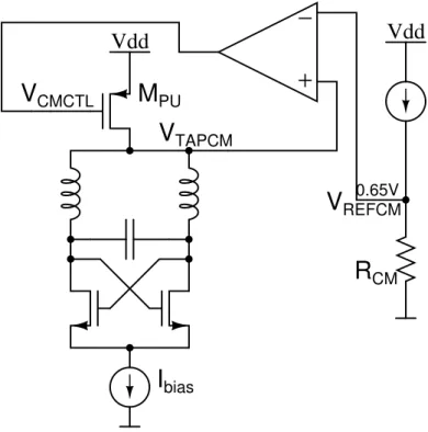
Figure
![Figure 1-4: Herzel, et al.’s, proposed topology to tune both the inductor and capacitor in an oscillator [2]](https://thumb-eu.123doks.com/thumbv2/123doknet/13791485.440468/26.918.335.588.387.799/figure-herzel-proposed-topology-tune-inductor-capacitor-oscillator.webp)


Documents relatifs
Then the global stability (observer + controller) is checked using theorem 5. The maximum numbers of packets lost for the two modes are 0 and 3 respectively while the system
The failures of control components may lead to a loss of the switching functions which handle the redundancy mechanisms between the process components. Hence we propose
The study of the question of the death penalty from different sides shows that the historically debated capital punishment in the United States is a real puzzle.The issues that make
The presented interval technique for the identification of invariant sets can easily be generalized towards the computation of the region of attraction of asymptotically
In order to do that, these different transformations must be applied: the discrete marking of places must be replaced by continuous marking; the delays associated
than one use it. This means that the more users adopt and contribute to a platform, the more valuable it becomes [6]. This is relevant in the big picture because most big data
Then, the voltage fluctuation levels are recorded in a sensitivity table (Fig. In the ICIM model, the IB is replaced by a simple monitoring of the voltage
Methods: We compared the estimations obtained by the Kaplan-Meier method and the competing risks method (namely the Kalbfleisch and Prentice approach), in 383 consecutive
