UNIVERSITÉ DE MONTRÉAL
MINIATURIZED OPTICAL PROBES FOR NEAR INFRARED SPECTROSCOPY
SREENIL SAHA
DÉPARTEMENT DE GÉNIE ÉLECTRIQUE ÉCOLE POLYTECHNIQUE DE MONTRÉAL
THÈSE PRÉSENTÉE EN VUE DE L’OBTENTION DU DIPLÔME DE PHILOSOPHIAE DOCTOR
(GÉNIE ÉLECTRIQUE) DÉCEMBRE 2018
UNIVERSITÉ DE MONTRÉAL
ÉCOLE POLYTECHNIQUE DE MONTRÉAL
Cette thèse intitulée :
MINIATURIZED OPTICAL PROBES FOR NEAR INFRARED SPECTROSCOPY
présentée par : SAHA Sreenil
en vue de l’obtention du diplôme de : Philosophiae Doctor a été dûment acceptée par le jury d’examen constitué de :
M. LEBLOND Frédéric, Ph. D., président
M. SAWAN Mohamad, Ph. D., membre et directeur de recherche M. LESAGE Frédéric, Ph. D., membre et codirecteur de recherche M. AUDET Yves, Ph. D., membre
DEDICATION
ACKNOWLEDGEMENTS
First of all, I would like to express my sincere gratitude to my advisers Professor Mohamad Sawan and Professor Frédéric Lesage, for their understanding, encouragement, and mentoring throughout my PhD studies. I also like to thank my committee members Professor Frédéric Leblond, Professor Yves Audet and Professor Frédéric Nabki for accepting to evaluate this thesis.
I would also like to thank Dr. Sascha Weyers of Fraunhofer IMS, Professor Eduoardo Charbon, Claudio Bruschini and Samuel Burri of Advanced Quantum Architecture Laboratory (AQUA) in École polytechnique fédérale de Lausanne (EPFL) for providing technical support.
Special thanks to all my friends in Molecular and Optical Imaging Laboratory and Polystim Neurotechnologies Laboratory, especially Yuankang Lu, Maxime Abran, Parikshat Sirpal, Samuel Bélanger, Sami Hached, Leila Montazeri, Mohammad Ali, Antoine Letourneau, Md. Hasanuzzaman and Elie Bou Assi, who were always there for me and made my study in Polytechnique one of the best experiences of my life. I would also like to thank Frederick Kalinain of Innotime Technologies for his support with fabrication.
I would like to gratefully acknowledge the help of one of my very special colleague, Laurent Mouden for his technical support and training in LASEM and Biostim labs. This work would have not been possible without his help and support. I am grateful to all the staff of Electrical engineering department of Polytechnique Montreal, especially Marie-Yannick Laplante, Réjean Lepage and Jean Bouchard for all their support. I am also grateful for the financial support from the Canada Research Chair on Smart Medical Devices and Optical Vascular Imaging, NSERC, ReSMiQ and CMC Microsystems.
Last but not least, I am grateful to my parents and my friends for their unconditional love, continued support and motivation throughout my studies. They always encouraged me to continue my goals and to go to the end of my ambitions.
RÉSUMÉ
L’étude de la propagation de la lumière dans des milieux hautement diffus tels que les tissus biologiques (imagerie optique diffuse) est très attrayante, car elle offre la possibilité d’explorer de manière non invasive le milieu se trouvant profondément sous la surface, et de retrouver des informations sur l’absorption (liée à la composition chimique) et sur la diffusion (liée à la microstructure). Dans la gamme spectrale 600-1000 nm, également appelée gamme proche infrarouge (NIR en anglais), l'atténuation de la lumière par le tissu biologique (eau, lipides et hémoglobine) est relativement faible, ce qui permet une pénétration de plusieurs centimètres dans le tissu. En spectroscopie proche infrarouge (NIRS en anglais), de photons sont injectés dans les tissus et le signal émis portant des informations sur les constituants tissulaires est mesuré. La mesure de très faibles signaux dans la plage de longueurs d'ondes visibles et proche infrarouge avec une résolution temporelle de l'ordre de la picoseconde s'est révélée une technique efficace pour étudier des tissus biologiques en imagerie cérébrale fonctionnelle, en mammographie optique et en imagerie moléculaire, sans parler de l'imagerie de la durée de vie de fluorescence, la spectroscopie de corrélation de fluorescence, informations quantiques et bien d’autres. NIRS dans le domaine temporel (TD en anglais) utilise une source de lumière pulsée, généralement un laser fournissant des impulsions lumineuses d'une durée de quelques dizaines de picosecondes, ainsi qu'un appareil de détection avec une résolution temporelle inférieure à la nanoseconde. Le point essentiel de ces mesures est la nécessité d’augmenter la sensibilité pour de plus grandes profondeurs d’investigation, en particulier pour l’imagerie cérébrale fonctionnelle, où la peau, le crâne et le liquide céphalo-rachidien (LCR) masquent fortement le signal cérébral.
À ce jour, l'adoption plus large de ces techniques optique non invasives de surveillance est surtout entravée par les composants traditionnels volumineux, coûteux, complexes et fragiles qui ont un impact significatif sur le coût et la dimension de l’ensemble du système. Notre objectif est de développer une sonde NIRS compacte et miniaturisée, qui peut être directement mise en contact avec l'échantillon testé pour obtenir une haute efficacité de détection des photons diffusés, sans avoir recours à des fibres et des lentilles encombrantes pour l'injection et la collection de la lumière. Le système proposé est composé de deux parties: i) une unité d’émission de lumière pulsée et ii) un module de détection à photon unique qui peut être activé et désactivé rapidement. L'unité d'émission de lumière utilisera une source laser pulsée à plus de 80 MHz avec une largeur d'impulsion de picoseconde. Cette source laser sera intégrée dans
la sonde avec l'unité de détection de lumière qui comprend des détecteurs à photon unique et d'autres circuits périphériques de commande. Le couplage de source / détecteur à petite distance, de préférence sur une seule puce, a le potentiel d’accélérer considérablement la méthode traditionnelle d’imagerie cérébrale portable.
ABSTRACT
The study of light propagation into highly diffusive media like biological tissues (Diffuse Optical Imaging) is highly appealing due to the possibility to explore the medium non-invasively, deep beneath the surface and to recover information both on absorption (related to chemical composition) and on scattering (related to microstructure). In the 600–1000 nm spectral range also known as near-infrared (NIR) range, light attenuation by the biological tissue constituents (i.e. water, lipid, and hemoglobin) is relatively low and allows for penetration through several centimeters of tissue. In near-infrared spectroscopy (NIRS), a light signal is injected into the tissues and the emitted signal carrying information on tissue constituents is measured. The measurement of very faint light signals in the visible and near-infrared wavelength range with picosecond timing resolution has proven to be an effective technique to study biological tissues in functional brain imaging, optical mammography and molecular imaging, not to mention fluorescence lifetime imaging, fluorescence correlation spectroscopy, quantum information and many others. Time Domain (TD) NIRS employs a pulsed light source, typically a laser providing light pulses with duration of a few tens of picoseconds, and a detection circuit with temporal resolution in the sub-nanosecond scale. The key point of these measurements is the need to increase the sensitivity to higher penetration depths of investigation, in particular for functional brain imaging, where skin, skull, and cerebrospinal fluid (CSF) heavily mask the brain signal.
To date, the widespread adoption of the non-invasive optical monitoring techniques is mainly hampered by the traditional bulky, expensive, complex and fragile components which significantly impact the overall cost and dimension of the system. Our goal is the development of a miniaturized compact NIRS probe, that can be directly put in contact with the sample under test to obtain high diffused photon harvesting efficiency without the need for cumbersome optical fibers and lenses for light injection and collection. The proposed system is composed of two parts namely; i) pulsed light emission unit and ii) gated single-photon detection module. The light emission unit will employ a laser source pulsed at over 80MHz with picosecond pulse width generator embedded into the probe along with the light detection unit which comprises single-photon detectors integrated with other peripheral control circuitry. Short distance source and detector pairing, most preferably on a single chip has the potential to greatly expedites the traditional method of portable brain imaging.
TABLE OF CONTENTS
DEDICATION ... iii
ACKNOWLEDGEMENTS ... iv
RÉSUMÉ ... v
ABSTRACT ... vii
TABLE OF CONTENTS ... viii
LIST OF TABLES ... xii
LIST OF FIGURES ... xiii
LIST OF ABBREVIATIONS ... xx
LIST OF APPENDICES ... xxi
CHAPTER 1 INTRODUCTION ... 1
1.1. Background ... 1
1.2. Research Hypothesis ... 3
1.3. Research Objectives ... 5
CHAPTER 2 LITERATURE REVIEW ... 8
2.1. Current functional neuroimaging techniques ... 8
2.1.1. Electroencephalography ... 8
2.1.2. Magnetoencephalography ... 9
2.1.3. Positron Emission Tomography ... 9
2.1.4. Magnetic Resonance Imaging ... 10
2.1.5. Functional Near Infrared spectroscopy ... 11
2.2. Light Emitters ... 14
2.3. Single and Multi-Photon Detectors ... 16
2.3.1. Photomultiplier Tube (PMT) and microchannel plates ... 16
2.3.2. PN Photodiode ... 17
2.3.4. Quantum dot photon detector ... 19
2.3.5. Superconducting Single Photon Detector ... 20
2.3.6. Schottky barrier photodiode ... 20
2.3.7. Avalanche Photodiode (APD) ... 21
2.3.8. Single Photon Avalanche Diode (SPAD) ... 21
2.4. Metrology ... 23
2.4.1. Passive Quenching and Recharge Circuit ... 23
2.4.2. Active Quenching and Recharge Circuit ... 26
2.4.3. Mixed Active-Passive Quenching and Recharge Circuit ... 27
2.4.4. Dark Noise ... 29
2.4.5. Photon Detection Probability (PDP) ... 32
2.4.6. Timing Jitter ... 33
2.5. Single Photon Avalanche Diode (SPAD) types ... 34
2.5.1. SPAD in custom process ... 34
2.5.2. SPAD in Standard CMOS Process ... 35
2.5.3. State-of-the-art SPADs fabricated in CMOS technology ... 36
2.6. RECENT NEAR INFRARED SPECTROSCOPY (NIRS) MODULES ... 43
2.6.1. Time-Gated Single Photon Counting Modules ... 43
2.6.2. CMOS-based SPAD sensors ... 45
2.6.3. Compact NIRS instrument employing light sources ... 51
2.6.4. Compact optical probes ... 53
2.7. Summary ... 54
CHAPTER 3 THEORY AND METHODOLOGY ... 56
3.1. Introduction ... 56
3.2. Proposed Gated Detector ... 57
3.4. Proposed Single Photon Detection Unit ... 63
3.5. Experimental Results... 64
3.6. Conclusion ... 66
CHAPTER 4 COMPACT FAST OPTODE-BASED PROBE FOR SINGLE-PHOTON COUNTING APPLICATIONS ... 67
4.1. Introduction ... 68
4.2. Architecture ... 69
4.3. Optical Probe Description ... 71
4.3.1. Light Emission Module ... 71
4.3.2. Fast Time-Gated Detection Block ... 72
4.4. Application Example ... 75
4.5. Conclusion ... 75
4.6. Acknowledgement ... 76
CHAPTER 5 COMPACT OPTICAL PROBE FOR TIME-RESOLVED NIRS-IMAGING .. 77
5.1. Introduction ... 78
5.2. System Description ... 80
5.3. Time-Gated Single Photon Detection module ... 82
5.3.1. Synchronization Block ... 82
5.3.2. Time Window Selection for Photon Detection ... 82
5.3.3. Variable Hold-off and Reset Pulse Generator ... 83
5.3.4. SPAD Front-end Electronics ... 84
5.3.5. High Electron Mobility Transistor based Driver ... 87
5.3.6. Analog Counter ... 89
5.4. Pulsed Light Emission Unit... 90
5.4.1. VCSEL Driver ... 90
5.5. Experimental Results... 92
5.6. Conclusion ... 100
5.7. Acknowledgement ... 101
CHAPTER 6 MINIATURIZED SIPM-BASED NIRS PROBE INTEGRATED WITH PULSED LASER SOURCE ... 102
6.1. Background ... 102
6.2. System Description ... 104
6.3. Single Photon Detection module ... 107
6.3.1. Generation of the Gated Counting Window ... 109
6.3.2. 2.5D Silicon Interposer Design ... 109
6.4. Pulsed Light Emission Unit... 112
6.5. Experimental Results... 113
6.6. Conclusion ... 117
6.7. Assessment ... 118
CHAPTER 7 GENERAL DISCUSSION AND RECOMMENDATIONS ... 119
7.1. Research Contributions ... 120
7.2. Recommendations and Future Works ... 121
CHAPTER 8 CONCLUSION ... 127
BIBLIOGRAPHY ... 129
LIST OF TABLES
Table 2.1. An overview of the strengths and limitations of fMRI, fNIRS and EEG ... 13 Table 2.2. Specifications of the various SPADs designed in CMOS technologies. All the values are reported at room temperature ... 42 Table 2.3. Comparison of the state-of-the-art SPAD imagers fabricated in CMOS 350 nm technology ... 51 Table 5.1. Parameters of Delay Block Architectures ... 83 Table 5.2. Comparison of the basic features of the various state-of-the-art NIRS systems ... 100
LIST OF FIGURES
Figure 1.1. Schematic illustration of the three modalities, (a) CW irradiation permits detection of light extinction, (b) TD irradiation monitors photon’s time of flight, and (c) FD
reconstructions are made from attenuation and phase shifts. ... 2
Figure 1.2. Showing the various layers of the brain, the late photons are mainly coming from the cortical region ... 3
Figure 1.3. Block diagram of the Proposed NIRS probe ... 5
Figure 2.1. Comparison of the characteristics of three common semiconductor light emitters ... 14
Figure 2.2. Construction of a Photomultiplier Tube (PMT) [36] ... 15
Figure 2.3. Cross-section of a p-n junction diode showing the various regions where electron-hole pairs can be generated along with their direction of flow [1] ... 16
Figure 2.4. Cross-sectional view of a PIN diode along with the energy band diagram, charge distribution and electric field distribution. ... 18
Figure 2.5. Schematic of a quantum dot photon detector [39] ... 19
Figure 2.6. Energy band diagram of a Schottky-barrier photodiode ... 20
Figure 2.7. Simple cross section of a Single Photon Avalanche Diode and its I-V curve ... 22
Figure 2.8. (a) Basic Passive Quenching Circuit (PQC) schematic (b) Equivalent SPAD model ... 23
Figure 2.9. Timing diagram during passive quench and recharge operation ... 25
Figure 2.10. (a) Basic schematic of a AQC (b) SPAD cathode voltage waveforms, connected to AQC ... 27
Figure 2.11. Basic schematic of a mixed active-passive quenching circuit ... 27
Figure 2.12. Timing diagram when using active quench and recharge operation ... 28
Figure 2.13. (a) Inter-avalanche time histogram highlighting contributions from primary and secondary pulses, (b) afterpulsing measurement using passive recharge, (c) afterpulsing measurement using active recharge ... 31
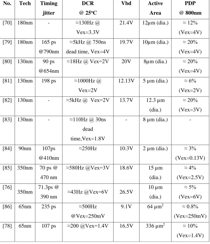
Figure 2.15. Cross-sectional view of a planar SPAD [1] ... 35 Figure 2.16. Cross-sectional view of a typical reach-through SPAD [1] ... 35 Figure 2.17. p+ /deep nwell SPAD fabricated in 180nm CMOS technology [69] ... 37 Figure 2.18. Schematic cross section of the device with a retrograde doping profile in 180nm CMOS technology [70] ... 37 Figure 2.19. SPAD Cross section implemented in 130nm technology [71] ... 38 Figure 2.20. Cross-section of the circular STI-bound SPAD 130nm CMOS technology [72] 38 Figure 2.21. CMOS back-side illumination-compatible SPAD reported in 90-nm imaging technology [73] ... 39 Figure 2.22. CMOS SPAD developed with an octagonal multiplication region in 90nm technology [74] ... 39 Figure 2.23. Cross-section of the SPAD in 0.35 μm CMOS technology [75] ... 40 Figure 2.24. Cross-section of the SPAD in 0.35μm CMOS technology, diameter of the active area are 10 µm-30 µm [76] ... 40 Figure 2.25. SPAD structure cross section - sensor was implemented in the 3D two-tier Tezzaron's FaStack [77] ... 41 Figure 2.26. p-well/deep n-well SPAD in 65/40 nm 3D IC CMOS technology [78] ... 41 Figure 2.27. (a) Block diagram of the fast-gating single-photon counting module [87] which includes the detection head and the control unit provides all the timing and trigger inputs/outputs, the USB link, (b) Windowed TO-8 package assembly, containing both active and “dummy” SPADs glued on a ceramic chip carrier. ... 44 Figure 2.28. Fast-gated module [88] consisting of two boards (left) and its housing (right) .. 45 Figure 2.29. (a) Chip carrier PCB with two chips bonded side by side for simultaneous operation at doubled resolution. The gap is less than 6 pixels wide [89]. (b) A block-level representation of the imaging system. The part on the right depicts the interior of the SPAD chip built around the central array of 128 x 512 pixels. An FPGA, depicted on the left, is used to generate the control signals and receive the data generated by the pixels. ... 45
Figure 2.30. Experimental setup showing the chip [90] with the peripheral circuits (b) Block diagram of the chip with interfacing board ... 45 Figure 2.31. (a) Micrograph of the fabricated 10×43 SPAD array [91], (b) 2D imaging set-up
... 46 Figure 2.32. Block diagram of the SPAD based smart pixel [93], showing the main components: SPAD detector, quenching circuit (VLQC), pulse shaper, coarse counter, fine interpolator, 16-to-4 encoder, memories and 10 bit output buffers. ... 48 Figure 2.33. Micrograph of the fabricated chip [94]; (b) A typical experimental Setup of the illumination measurement ... 48 Figure 2.34. Micrograph of the sensor chip and photograph of the detection system [96] ... 49 Figure 2.35. (a) Photomicrograph of the CMOS single-photon image sensor(8x5mm2) [97], (b) Experimental setup of the overall LIDAR system. ... 49 Figure 2.36. (a) Block diagram of the complete system [106] consisting of two pulsed laser sources (at 670 nm and 830 nm), one 1 mm2 active area SiPM based single-photon detection module and a TDC-based TCSPC system to reconstruct the optical waveform and send it to a portable PC for data analysis, (b) Picture of the instrument enclosed in an aluminum box of size 200 × 160 × 50 mm3, which hosts three fiber ports on front side and other connectors (power supply, USB, and trigger IN/OUT) on the rear panel. ... 52 Figure 2.37. (a) Complete two-chip micro-system [107]. The PCB daughter card is physically supported by the filter and sample holder and stacked header pins, (b) AlInGaN micro-LED array bump-bonded to an 8 × 8 CMOS driver array. ... 52 Figure 2.38. (a) Scheme of the experimental setup employed to operate the probe [109] based on small (5 mm) source-detector separation. (b) The probe (shown in photo) was positioned over the sensorimotor area of the left hemisphere demonstrating its effective utilization. ... 53 Figure 2.39. (a) Picture of fNIRS IC-based portable fNIRS system [110], (b) Architecture of HMS-based fNIRS system ... 54 Figure 3.1. Proposed Gated Mode Description ... 58
Figure 3.2. (a) Applying a gate ensures that the detector is active when the photon of interest arrives, even if the detector is constantly being illuminated. (b) Applying a gate ensures
that the detector is not blinded by the preceding strong pulse ... 58
Figure 3.3. Illustration of the sensitivity of different source-detector separations, modeled and simulated by Monte Carlo, using fluorescent light propagation in the defined multilayers diffusive medium ... 61
Figure 3.4. Comparison of the Sensitivity profiles for the classical approach (ρ = 40mm) and for the novel approach (ρ = 1mm) (a) no Time gating, (b) detecting photons after 400ps and (c) 600ps ... 62
Figure 3.5. Complete block diagram of proposed Gated Single Photon Detection Unit ... 63
Figure 3.6. (a) Count rate distribution for 5ns and 10ns gate-ON time window, (b) Dependence of Photon count rate on the Gate window ... 65
Figure 3.7. (a) Count rate when SPAD and Laser source are separated by 6mm and 52mm (b) Count rate vs Source-Detector distance ... 65
Figure 4.1. Simplified block diagram of the proposed optical probe ... 68
Figure 4.2. Photograph of the Proposed Optical Probe ... 69
Figure 4.3. Light-Current-Voltage (LIV) module exhibits an optical to electrical conversion efficiency of 5mW/V. Inset is the schematic of the VCSEL driver ... 70
Figure 4.4. The measured optical waveforms, below shows the zoomed section ... 70
Figure 4.5. Simplified block diagram of the Fast-Gated Detector Module with the integrated counter ... 71
Figure 4.6. Photon counts distribution within a 5 ns gate-ON time window. ... 72
Figure 4.7. Dependence of the SPAD count rate on the input photon flux ... 73
Figure 4.8. Stability of the module count-rate over a time range of 1 hour. ... 73
Figure 4.9. Time-of-Flight experiment with the compact module ... 74
Figure 5.1. Block Diagram of the Compact Optical Probe ... 80
Figure 5.2. Schematics of the Synchronization Block ... 81
Figure 5.4. Proposed Hold-off Time and Reset Pulse Generator ... 83
Figure 5.5. SPAD frontend electronics (a) Simplified block diagram, (b) SPAD structures [95] ... 84
Figure 5.6. Integrated Comparator (a) Simplified Schematics, (b) Simulated comparator output with different threshold voltages ... 85
Figure 5.7. Two-phase charge pump (a) Schematics of single stage, (b) Relation between the derived output voltage and the number of stages ... 85
Figure 5.8. High-voltage level shifter to provide a suitable biasing voltage to the SPAD (a) Schematics of the integrated level shifter, (b) Ouput voltage pulse of the high-voltage level shifter ... 86
Figure 5.9. High Voltage pulser to have sub-nanoseconds transition times ... 87
Figure 5.10. Proposed Analog Counter (a) Simplified Schematics, (b) Timing Diagram showing the voltage levels at the various nodes ... 88
Figure 5.11. Simulations results of the analog counter (a) Transient simulations of the output voltage, (b) Output voltage step size vs the Count Rate ... 89
Figure 5.12. Proposed VCSEL driver Circuit (a) Simplified Schematics, (b) Graph showing the simulations of the VCSEL driver circuit, top - CMOS-level input voltage pulses, bottom - the current mode signals ... 90
Figure 5.13. Proposed System-In-Package (SiP) Optical probe (a) QFN package of dimensions 12 x 12 mm2, (b) Control Chip, (c) SPAD structures of 10u, 20u and 30u active areas, (d) VCSEL chip, (e) Overall module, housed in a 2 x 1.5-inches enclosure ... 91
Figure 5.14. The measured optical waveforms. The driving input voltage amplitude varies between 1.0 and 3.0 V. ... 92
Figure 5.15. Output frequency as a function of the control voltage ... 93
Figure 5.16. Voltage waveforms during the module operation ... 94
Figure 5.17. Output voltage of the 2-phase charge pump vs clock frequency ... 95
Figure 5.18. (a) Differential Non Linearity of the analog counter, (b) Integral Non Linearity of the analog counter ... 96
Figure 5.20. Photon counts distribution within a 5 ns gate-ON time window, when the SPAD is
gated at 40 MHz with an excess bias voltage of 5 V. ... 98
Figure 5.21. Time-response of the time-gated module to the integrated pulsed VCSEL source, with 350 ps pulse-width ... 99
Figure 5.22. Count rate plot during heart-beat measurements by illuminating the index finger of the volunteer ... 99
Figure 6.1. The geometry of TD NIRS measurements also depicts the region where photon paths are more likely to occur (so called “banana shape”) ... 102
Figure 6.2. Compact Optical Probe, (a) Simplified Block Diagram, (b) System level integration on a silicon interposer platform ... 106
Figure 6.3. Scheme of the current mode approach where the SiPM current can be mirrored for both amplitude and timing measurement purpose ... 106
Figure 6.4. Simplified schematic of the Transimpedence Amplifier 1 ... 107
Figure 6.5. Simplified schematic of the Transimpedence Amplifier 2 ... 107
Figure 6.6. (a) Gate Shaper, (b) Voltage signal at the various nodes ... 110
Figure 6.7. Cross-sectional view of the Silicon Interposer Platform with the layer definitions ... 110
Figure 6.8. Silicon Interposer Platform (module 3) (a) Bare dice directly bonded to the silicon interposer along with other ancillary components for a high density multitechnology System-in-Package design, (b) Simplified layout of the proposed platform using Tanner EDA tool ... 111
Figure 6.9. Proposed VCSEL driver circuit ... 111
Figure 6.10. Proposed Optical probe, (a) Miniaturized version with the control chip, SiPM, VCSEL chip and peripheral capacitors integrated on 2.5D silicon interposer platform having a size of 1 x 1 cm2, (b) PCB Module – control chip, SiPM and VCSEL are enclosed in separate packages and soldered onto a PCB ... 114
Figure 6.11. Stability analysis (a) linearity of the emitted optical power, (b) Variation of the temporal widths of the recorded curves ... 115
Figure 6.12. The measured optical waveforms. The driving input voltage amplitude varies
between 1.0 and 3.0 V ... 115
Figure 6.13. Relation between the output frequency as a function of the control voltage ... 116
Figure 6.14. Measured IRF of the module with an emitted laser pulse width of 5ns ... 117
Figure 6.15. Stability of the module count-rate over a time range of 1 hour ... 117
Figure 6.16. Time-of-Flight experiment with the compact module ... 118
Figure 7.1. System block diagram showing an optical trigger module, pulse width control units, on-chip delay lines, binary trees, pulse generators (PGs), and 32 groups of SPAD array ... 124
Figure 7.2. SPAD gating frontend circuit ... 125
Figure 7.3. SPAD anode voltage waveforms during photon detection and no-detection ... 126
LIST OF ABBREVIATIONS
NIRS Near Infrared Spectroscopy
NIR Near Infrared
TD-NIRS Time Domain Near Infrared Spectroscopy
DTOF Distribution of Time of flight
SPAD Single-Photon Avalanche Diode
ns-SDD Null/Small Source-Detector Distance
TCSPC Time-correlated single-photon counting
SiPM Silicon Photomultiplier
SiP System-in-Package
SoC System-on-Chip
VCSEL Vertical Cavity Surface Emitting Laser
LED Light Emitting Diode
APD Avalanche Photodiode
APP After Pulsing Probablity
DCR Dark Count Rate
PDP Photon Detection Probablity
FWHM Full Width at Half Maximum
PQC Passive Quenching Circuit
AQC Active Quenching Circuit
QE Quantum Efficiency
CMOS Complementary Metal Oxide Semiconductor
TG Time-Gated
LIST OF APPENDICES
CHAPTER 1
INTRODUCTION
1.1. Background
The study of light propagation into highly scattering and diffusive medium is quite fascinating and has proven to be an effective method to explore the medium non-invasively and gather information relating to its chemical composition and microstructure [2-4]. Since the last decade researchers have shown an increasing interest in the near-infrared (NIR) spectral range (600 – 1000 nm) because the light attenuation by the biological tissue constituents (eg., water, lipid, and hemoglobin) in this wavelength range is relatively low which allows for the penetration through several centimeters of tissues (eg., muscle and brain cortex) [5-7]. The Near InfraRed spectroscopy (NIRS) technique involves the use of a point source to inject a light signal (few mW) into the media and the diffused photons or the emitted signal, carrying information on tissue constituents, are collected by a detector placed at a given distance from the source [8-10]. The analysis of the collected light, or the number of detected photons, which emulates the difference in the absorption spectra of oxygenated and deoxygenated hemoglobin, allows for the measurement and derivation of the hemodynamic parameters such as oxy-hemoglobin concentration (HbO2), deoxy-hemoglobin concentration (HHb), total hemoglobin concentration (tHb = HHb + HbO2) and blood oxygen saturation (SO2 = HbO2 / tHb). Thus, the photon migration phenomena, happening due to the complex interplay between the light absorption and light scattering, can be exploited for a wide variety of clinical applications such as functional brain imaging, molecular imaging, muscle oximetry, optical mammography, study of osteoporosis, fluorescence lifetime imaging (FLIM), fluorescence correlation spectroscopy (FCS), quantum information and many others.
A typical NIRS setup utilizes a light source such as laser diode or light-emitting diode (LED), having an emission wavelength spanning between 600 and 1000 nm, a detector, e.g. a photodiode, to detect the incoming light and flexible fiber optics for light delivery and collection from the tissues. Three different NIRS techniques can be employed to probe medium (Fig. 1.1):
(i) Continuous Wave (CW) NIRS is the simplest technique which requires the use of inexpensive laser diodes or even LEDs acting as a steady-state light source whose emission amplitude can be varied at a very low frequency (few kHz), and a highly sensitive detector such as an avalanche photodiode to detect the minute changes in the light intensity which
(a) (b) (c)
Figure 1.1. Schematic illustration of the three modalities, (a) CW irradiation permits detection of light extinction, (b) TD irradiation monitors photon’s time of flight, and (c) FD reconstructions are made from attenuation and phase shifts.
reflect changes in the relative concentration of hemoglobin. But the disadvantage of CW systems is that they cannot differentiate between light absorption and scattering, hence HbO2 and HHb concentrations cannot be computed in absolute terms.
(ii) Frequency domain (FD) NIRS is composed of a modulated light source which modulates the emitted light intensity (at frequency of the order of 100 MHz up to 1 GHz) and a detection system capable of demodulation to measure the intensity of the incoming light as well as the phase shift which corresponds to the time of flight. The advantage of FD NIRS systems is that they can be easily miniaturized, and the measurements can be used in various ways to compute absorption and scattering properties. As compared to CW-NIRS systems, FD is more expensive but less than the Time Domain (TD) systems. Its accuracy is also between TD and CW systems.
(iii) Time Domain (TD) NIRS employs a pulsed light source, typically a laser source emitting light pulses with a duration ranging from a few tens of picoseconds down to femtoseconds, and a detection module with sub-nanosecond temporal resolution, placed at a certain distance from the light injection point, to measure the photon distribution of time of flight (DTOF). The DTOF (also known as the temporal point spread function, TPSF) is essentially subjected to the same physical phenomenon which translate in delaying, broadening and attenuating. The delay is the result of the finite time taken by the injected photons to reach the detector, broadening is due to multiple scattering resulting in the different paths the photons undergo, attenuation happens because of absorption and diffusion that significantly decreases the number of detected photons. TD techniques can provide better sensitivity and penetration depth by relying on its ability to measure the photon DTOF and exploiting the timing information of scattered and re-emitted photons.
Figure 1.2. Showing the various layers of the brain, the late photons are mainly coming from the cortical region
Henceforth, TD-NIRS systems has an inherent advantage of providing a better accuracy and spatial resolution by yielding the highest amount of information about the migration of photons through tissues, clearly making it a better choice than the cheaper but inaccurate CW and FD systems. This thesis aims to demonstrate a standalone TD-NIRS system integrated with pulsed light emission and single photon detection units, both placed very close to each other preferably on a single substrate. The light emission unit comprises a pulsed laser source with pulse width of tens of picosecond and a repetition rate of over hundreds of MHz and the detection unit is based on a fast time-gated technique to detect the impinging photons in some specified time windows. The proposed module can be integrated in any experimental setup and is easily configurable by means of a simplified user interface for bidirectional communication with a remote computer.
1.2. Research Hypothesis
In TD NIRS increasing the source–detector distance [11] not only results in an increased delay and broadening of the DTOF but also decreases the number of detected photons, as observed in the case when the scattering increases. The absorption doesn’t have any substantial impact on the temporal position of the DTOF but affects both the signal intensity and the trailing edge (i.e., slope of the tail) of the DTOF. A major misconception in TD NIRS is that penetration depth is dependent on source-detector separation, like in CW NIRS. On the contrary, for an absorbing point-like inclusion embedded in a homogeneous medium, it was demonstrated that the approach based on null source-detector distance yields better spatial resolution and contrast as compared to that of large source-detector separations [12, 13]. The same observation holds true for absorption and scattering inclusions with finite dimensions or layered geometries which
closely mimics some biological structures, such as head or muscle. An innovative and ground-breaking approach to TD NIRS reflectance measurements, based on null source–detector separation, exhibits some significant advantages over the classical TD NIRS approach (fixed source and detector at a large distance) by avoiding the inaccurate description of light propagation due to the photon diffusion at early time and short distance. One of the key requirement is to increase the sensitivity to higher penetration depths of investigation, in particular for functional brain imaging, where skin, skull, and cerebrospinal fluid (CSF) heavily mask the signal coming from cortical regions. Figure 1.2 presents the basics of TD NIRS, illustrating the effect of source detector distance, absorption, and reduced scattering in a diffusive medium, which is an oversimplification of the real geometry of a human head [14]. Generally, Time-correlated single-photon counting (TCSPC) is the used technique to measure fast light pulses at the single-photon level especially if coupled with silicon single-photon avalanche diodes (SPADs) [15].
Even though the null/small source-detector distance (ns-SDD) configuration is the one that has highest sensitivity to deep tissue, since detected photons propagate a shorter path, detector dynamic range limits its applicability. Even with a time-domain single-photon technique, photon pile-up with increasing illumination power limits sensitivity to late photons leading to long integration times. The detector gating technique [15-18] for TCSPC allows probing at depth with small source-detector distance by rejecting the large signal/early photons from the surface which, considering the limited dynamic range of detectors, otherwise restricts the sensitivity of the probe to the vicinity of its tip. In this work, we will exploit unique expertise in microelectronic design of integrated circuits to develop a novel integrated electronic and optical design, incorporating functionalities such as time-gated detection and pulsed-laser illumination within a single chip, a feat that remained out of reach until now. Miniaturization is possible as our probes will use detector and laser source side-by-side, leading to a very small source detector distance, which will not only allow interrogating deeper tissue volumes (cortical surface) with late time gates but also integrating early gates to monitor surface physiology (skin, bone) and remove its contributions to deep signals.
Figure 1.3. Block diagram of the Proposed NIRS probe 1.3. Research Objectives
With decreasing source detector distance, several technological issues should be taken into account and the most severe obstacle is the presence of early photons which increase at a much faster pace than the late photons and may eventually saturate the detection electronics, thus preventing the extraction of long-lived photons that carry useful information from deep structures. Hence, to fully exploit the advantages of the TD null source-detector distance approach, an efficient mechanism should be implemented to gate, or at least to reduce burst of early photons.
The long term goal for this research project is the development of a miniaturized optode device, as illustrated in Fig. 1.3, integrated with both laser source and single photon detector primarily for the purpose of portable brain imaging, having the capability of mapping and understanding the functioning of the human brain cortex and can also be effectively utilized in the applications such as optical mammography and fluorescence lifetime imaging. In order to achieve the long term goal as described earlier, the project has been divided into the following three specific objectives which are accomplished during this research:
Objective 1: Design a single photon counting setup for preliminary testing and getting accustomed with the overall optical experimental setup and performing time-gating of pulsed laser sources. For ease of testing and proof-of-concept, a compact PCB based standalone system, integrated with time-gated single photon counting module and a pulsed light emission unit, was developed using off the shelf discrete components. The module was made user-configurable via a Universal asynchronous receiver-transmitter (UART) interface and can be integrated in any optical setup.
Hypothesis 1: The source-detector separation affects the investigation depth and should be reduced to increase the number of collected photons which has a positive effect on the signal-to-noise ratio and image contrast. On the other hand, the decrease in source-detector distance also increases the number of unwanted early arriving photons, so the time-gated detection scheme should be adopted to extract information from late photons.
Related Publication:
S. Saha, F. Lesage, and M. Sawan, "Time-resolved reflectance using short source-detector separation," in Circuits and Systems (ISCAS), 2016 IEEE International Symposium on, 2016, pp. 333-336: IEEE
Objective 2: Design a miniaturized system-in-package (SIP) optode equipped with pulsed laser source as light emitting unit and fast time-gated single photon counting module as light detection unit capable of detecting photons in specific time windows, thus enabling the measurement of very faint optical signals.
Hypothesis 2: The novel time-gated detection approach has paved the way to the development of null-distance source detector optode that is easier-to-handle, convenient for cap design and could yield a simplified image reconstruction. The developed compact probe can be seen as a standalone time-resolved near-infrared spectroscopy system and has potential for widespread exploitation, especially for brain measurements where smaller optical probes eliminates the need for optical fibers for light injection and collection, making the measurement process more practical.
Related Publication:
S. Saha, Y. Lu, S. Weyers, M. Sawan, and F. Lesage, "Compact Fast Optode-based Probe for Single-Photon Counting Applications," IEEE Photonics Technology Letters, 2018.
S. Saha, F. Lesage, and M. Sawan, "High-voltage pulse generator with variable delay for ultrafast gating of single photon detector," in Circuits & Systems (LASCAS), 2016 IEEE 7th Latin American Symposium on, 2016, pp. 131-134: IEEE
S. Saha, Y. Lu, S. Weyers, F. Lesage, and M. Sawan, " Miniaturized Probe for Time-Domain Near-Infrared Spectroscopy," has been accepted for lecture presentation at the Biomedical Circuits and Systems Conference (BioCAS), 2018 IEEE, Cleveland, Ohio USA from October 17-19.
S. Saha, Y. Lu, S. Weyers, F. Lesage, and M. Sawan, “Compact Optical Probe for Time-resolved NIRS- Imaging,” under review in IEEE Transactions of Circuits and Systems I: Regular Paper.
Objective 3: Develop a compact fiber-free optical probe integrating silicon photomultiplier and light-pulsing unit, which can be directly put in contact with the sample under test without the need for cumbersome optical setup.
Hypothesis 3: The integrated circuit, assembled on a 2.5D silicon interposer platform of size 1 cm interfaced with other ancillary components such as capacitors and resistors, leads to significant optode-size reduction and the elimination of optical fibers and has the potential to change the landscape of Near Infrared Spectroscopy (NIRS) hardware commercially. The introduction of silicon photomultipliers (SiPM) would result into high diffused photon harvesting efficiency.
CHAPTER 2
LITERATURE
REVIEW
This chapter first provides an overview about the various neuroimaging techniques, followed by an illustration of the the characteristics and working principle of the various building blocks/elements of the NIRS module. The various functional units presented in this chapter are viewed individually based on the literature and from the knowledge garnered during the course of this thesis work. To comprehend the basic features and adopt the best possible choice, a brief comparison between the various light emitters and single photon detectors is presented. Also, the physics behind the various photodetectors is briefly explained to understand the characterization procedures and parameters. This chapter also demonstrates how single-photon detectors can be fabricated in commercial deep-submicron complementary metal oxide semi-conductor (CMOS) processes, for miniaturization with low dark noise, while comparing the various state-of-the-art structures implemented so far. The quench and recharge circuitry for the single photon detectors are briefly discussed.
Chapter organization: Section 2.1 briefly describes the various brain imaging modalities, including their strengths and limitations associated with the various techniques. Section 2.2 presents the comparison of the various light emitters. Section 2.3 presents the various multi and single photon detectors. Section 2.4 illustrates the passive and active techniques used to perform the quench and recharge operations and the SPAD fundamentals. Section 2.5 provides a short comparison of the various SPADs designed and fabricated in various standard CMOS process. Section 2.6 presents some of the recent state-of-the-art NIRS systems. Section 2.7 summarizes the chapter.
2.1. Current functional neuroimaging techniques
2.1.1. Electroencephalography
Electroencephalography (EEG) is the earliest and most utilized functional neuroimaging technique for the recording of electrical activity along the scalp produced by the firing of neurons within the brain. The abnormal neural activities are visualized by means of multiple electrodes placed on the scalp which continuously record voltage fluctuations resulting from ionic current within the neurons. EEG plays a vital role in epilepsy diagnosis [19] and in determining seizure types, and thereby in choosing anti-epileptic drug (AED) and predicting
prognosis. EEG has also been validated as a reliable tool in the localization of the epileptic focus area [20]. Focal epileptiform abnormalities can be clearly distinguished from background on EEG. Extensive research has been conducted to assess the feasibility of monitoring EEG signals for automatic seizure onset detection. Furthermore, analysis of EEG signals both in the time and frequency domain enables the study of functional connectivity network in epilepsy [21].
EEG has some inherent disadvantages, for example, in scalp EEG the signal is attenuated (sometimes even cancelled) by soft tissues/bone and frequently degraded by muscle artifacts resulting in the decrease of sensitivity in the detection of epileptic events. A large area of the cortex has to be activated synchronously to generate enough potentials to be able to be detected by a scalp electrode [22]. Even invasive intracranial EEG is limited in both sampling time and area while increasing the risk for possible complications such as bleeding or infection. On major limitation of EEG monitoring is that it does not provide information on blood volume and oxygenation which could help in the evaluation of the metabolic impact of seizures.
2.1.2. Magnetoencephalography
Magnetoencephalography (MEG) is a noninvasively functional neuroimaging technique that can measure the weak magnetic fields resulting from the intracellular current flow within neurons at a high spatiotemporal resolution [23]. In contrary to scalp EEG, MEG signal is less affected by distortion from the skull and intervening soft tissue [24]. The main clinical use of MEG in epilepsy is to detect and localize the source of pathological activity in patients [25]. However, MEG often has poor sensitivity in recording paroxysmal activity within the mesial structures of the brain because of the rapidly decaying magnetic fields associated with medial discharges [26]. Furthermore, MEG is also not suitable for long-term recording, making it challenging or almost impossible to record seizures.
2.1.3. Positron Emission Tomography
Positron Emission Tomography, popularly known as PET, is an innovative and relatively new form of medical diagnostic imaging technique that has begun to be adapted in a clinical setting since the early 1990s and is used by physicians to examine biochemical changes occurring within a patient. A PET imaging can be used as a diagnostic imaging tool by the physicians to
examine biochemical changes occurring within a patient. As the diseases usually affect the biochemistry of a patient and PET can be effectively utilized to detect these changes. A metabolic PET scan is used to diagnose, stage and follow-up on the treatments by examining a patient’s biochemistry. PET scans can detect diseases making it an effective diagnostic tool, thanks to its ability to study bodily functions through biochemical processes. PET imaging helps in the study of metabolic functions of a patient and hence can be used to guide biopsies and also other exploratory surgeries conducted to distinguish between benign (non-cancerous) and malignant (cancerous) tumors. It can determine how far a disease has spread and reduce the number of unnecessary surgeries performed due to incorrect diagnosis and staging data. It can also be effectively used for the diagnosis of early stages of certain neurological illnesses such as Alzheimer’s disease, epilepsy and other mental illnesses. For individuals afraid of getting infection from medical procedures, PET scan is perhaps the best option.
Regardless of its numerous advantages, PET scans also have its disadvantages. The radioactive component used during PET procedure may pose some risk. Even though the radioactive components used in PET imaging are not long lasting but there is only a limited amount of times a patient can undergo this procedure as it may not be suitable for some patients and may cause some complications if the patients are pregnant. Since it is a relatively new procedure, PET imaging is quite expensive compared to other forms of medical imaging. Also, PET scans are not offered in the majority of medical centers in the world. Another problem with PET imaging is that the sensitivity is so high that even if a patient is suffering from chemical imbalance due to diabetes and it may trigger false imaging results.
2.1.4. Magnetic Resonance Imaging
The physical principle of magnetic resonance imaging (MRI) is based on the directional magnetic field, or moment, associated with charged particles in motion. All atomic nuclei containing an odd number of protons and/or neutrons possess an intrinsic magnetic moment or precession. Because nuclei are charged particles, this precession produces a small magnetic moment. When a human body is placed in a large magnetic field, majority of hydrogen nuclei align parallel to the magnetic field.and rotate with a frequency proportional to the applied magnetic field strength. Next, an exposure to radio-frequency (RF) pulse at the same frequency as that of the precessing hydrogen nuclei results in non-invasive displacement of the nuclei.
Once the RF signal is removed, the nuclei realign themselves and return to equilibrium by emitting their own RF signal referred to as the free-induction decay (FID) response signal. The FID response signal is then measured by a conductive field coil placed around the object, then reconstructed to obtain 3D grey-scale MR images. Functional MRI (fMRI) has made it possible to examine active brain regions, apart from structural imaging of the brain, by relying on the blood oxygen level dependent (BOLD) contrast. The deoxygenated blood is paramagnetic (attracted to an external magnetic field) while the oxygenated blood is diamagnetic (repelled from an applied magnetic field) [27, 28]. Thus, the difference in magnetic susceptibility of deoxygenated and oxygenated blood helps in the derivation of the source of the BOLD contrast, which serves as a proxy measure of the neural activation elicited by a stimulus [29].
Many of the reasons that have resulted in the emergence of fMRI BOLD as a popular choice are it is non-invasive, repeatable, widely available and possesses superior spatial resolution. Furthermore, this technique provides high-resolution activation maps that is more accessible to non-expert audiences and allows for visually communicable results. However, fMRI also has a number of disadvantages such as contraindications to being in a magnetic field (e.g., metal in the body from a previous surgery), claustrophobia, restrictions on movement, the typical supine position of subjects, the requirement for compatible response equipment, and the noise produced by the scanner [30]. Furthermore, given the high costs required to maintain the equipment and employ technicians to operate the scanner, functional MRI studies can be quite expensive.
2.1.5. Functional Near Infrared spectroscopy
Functional Near Infrared spectroscopy (fNIRS) is a modern non-invasive optical imaging technique that can be used to measure changes in hemoglobin (Hb) concentrations in brain tissue. fNIRS relies on the different absorption properties of biological chromophores to measure the hemodynamic response to neural activity, unlike fMRI which relies on the paramagnetic properties of Hb [4, 28, 31]. Near infrared spectrum of the light (between 600 nm and 1000 nm) easily penetrates through biological tissues because only a few biological chromophores absorb light at these wavelengths. Changes in chromophore concentrations can be calculated according to the modified Beer-Lambert law. The absorption spectra of Hb vary in its oxygenation state and so the amount of NIR light transmitted through the tissue results in
the measurement of oxygenated Hb (oxy-Hb) and deoxygenated Hb (deoxy-Hb) and information about the oxygenation-deoxygenation states can be derived. Functional NIRS has proven to be a promising technology as an independent functional neuroimaging method or for use in conjunction with MRI and fMRI and can be utilized across a wide range of areas. fNIRS has also been used to investigate the hemodynamic response during activities such as walking, exercise and other everyday tasks, which otherwise cannot be measured within a fMRI scanner. Commercial clinical fNIRS instruments were first available in 1989 but more recently advanced systems with multiple probes have enabled broader use in research and clinical practice.
Functional NIRS has a number of advantages in terms of its utility that make it an ideal choice for interrogating brain function. fNIRS is non-invasive, relatively inexpensive, and has a temporal resolution that is comparable to that of fMRI [32]. Recent technological advancements have resulted in development of portable modern fNIRS devices that are miniaturized, wireless and battery-operated which relaxes the need for strict restrictions on motion [33]. fNIRS has allowed for advancements in the study of neurocognitive processes in unconstrained environments, including studies outdoors and in various other ambulatory settings. Even though fNIRS signals are still sensitive to degradation due to motion artifacts but several several groups have elaborated on methods for real-time motion correction that makes fNIRS an attractive alternative, particularly for people where complete stillness can be extremely challenging (eg., infants). Furthermore, other significant advantages of fNIRS include insensitivity to common electrical or magnetic devices, such as hearing aids, pacemakers, or cochlear implants, and ease of integration with other neurocognitive applications. Recent technological advances have centered on the combined technological and functional uses of fNIRS and EEG or fMRI, with the goal of advancing brain-computer interface technologies.
The main limitations of fNIRS as a clinical neuroimaging tool relate to physical and technological constraints imposed by the device setup, for eg., the size of the measurable brain area strongly depends on the number of sources and detectors in the fNIRS setup. Another key limitation is that fNIRS is only able to detect NIR light that penetrates the first few centimeters of cortical tissue. fNIRS signals are also prone to be contaminated by physiology-based interference from cardiac pulsation, respiration, spontaneous changes in local vascular tone and a variety of spontaneous low frequency oscillations, hence a variety of processing methods are needed to be adopted to remove these frequencies from the data [34, 35]. Moreover, fNIRS
signals also contain superficial scalp signals embedded in the, more desired and useful, ‘‘brain signal’’. An overview of strengths and limitations associated with fMRI, fNIRS and EEG is listed in Table 2.1.
Table 2.1. An overview of the strengths and limitations of fMRI, fNIRS and EEG Modalities
Parameters
fMRI fNIRS EEG
Strengths ✓ Non-invasive ✓ Repeatable ✓ Widely available ✓ Superior spatial resolution ✓ Whole brain measurement (lateral surface and depth) ✓ Non-invasive ✓ Repeatable ✓ Comparable temporal resolution to fMRI ✓ Inexpensive ✓ Portable ✓ Less restriction on motion ✓ Invasive/Non-invasive ✓ Reliable tool in the localization of the epileptic focus area ✓ Focal epileptiform abnormalities can be clearly distinguished from background Limitations • Expensive • Strict restrictions of motion • Need for supine
position • Noisy scanner • Physiological noise • Restrictions based on metal in the body • Limited to frontal regions and surface analysis • Physiological noise (including superficial scalp signals) • Lacks anatomical information • Interpretation challenges related to multiple sources of vascular signal • Signal attenuation by soft tissues/bone • Muscle artifacts results in the decrease of sensitivity
• Large area of the cortex to be activated • Doesn’t provide
information on blood volume and oxygenation
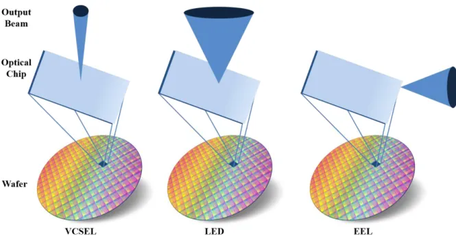
Figure 2.1. Comparison of the characteristics of three common semiconductor light emitters 2.2. Light Emitters
Over the years, semiconductor light emitters have emerged as ideal and vital light sources for a wide range of biomedical sensing/imaging applications and can be commonly classified to be of three types – vertical cavity surface emitting laser (VCSEL), light emitting diode (LED) and edge emitting laser (EEL). Among them VCSEL is a relatively recent entrant to the list of choices of semiconductor light-emitting devices. Figure 2.1 illustrates the basic differences in the characteristics of the three types of commonly used optical sources. All three types of semiconductor devices are fabricated by growing epitaxial III-V semiconductor layers (such as GaAs, AlGaAs, InP, or InGaAsP) on a GaAs or InP substrate. The wafers are processed through several photolithographic steps to define the individual devices, such as etching ridges, depositing and patterning metal contacts, or depositing and patterning dielectrics. A LED is created by incorporation a p-n junction in the epitaxially grown layers whereas laser typically requires a feedback mechanism which is implemented by means of mirrors sandwiching the gain region. In an EEL this is achieved by cleaving the wafer, and the cleaved edges form the parallel mirrors of the device which results in light emission from the cleaved edge of the wafer. Hence, EEL devices cannot be tested at the wafer level and the wafer has to be diced to test the individual lasers. In case of VCSEL, mirrors with sufficient reflectivity are grown or deposited on the wafers, sandwiching an active region which results in vertical light emission from the wafer. Both the VCSEL and LED typically emit light from the top surface of the wafer, and so they can be tested at the wafer level by probing bond pads accessible at the surface of the wafer.
Figure 2.2. Construction of a Photomultiplier Tube (PMT) [36]
In addition to the manufacturing advantage of wafer scale testing, VCSEL also exhibits a lot of performance advantages as compared to the low cost LEDs or EELs which can be listed as follows:
1. Integrability: Semiconductor manufacturing and wafer integration of VCSELs is compatible with other optical devices such as detectors and other circuitry.
2. Scalability: VCSELs can be easily fabricated on a single chip into one and two dimensional arrays to scale optical output power matching some specific applications.
3. Packageability: VCSELs allow the use of low-cost packaging as that of LEDs or EELs to reduce cost, thus providing the option of replacing the LEDs in the existing applications. Also, VCSELs are compatible with chip-on-board technology and other custom packaging techniques that greatly simplifies system integration.
4. Low Power: Power consumption is extremely low which increases the efficiency, battery life and thermal design constraints in larger systems.
5. High efficient optical beam: It emits coherent, symmetrical and low divergent optical beam with a narrow spectral width.
Two-dimensional arrays of VCSELs can be flip-chip attached or wire-bonded to CMOS integrated circuits, thus providing major opportunities in both miniaturization and hybrid integration of multiple heterogenous chips. Optical interconnects based on CMOS/VCSEL technology have been widely proposed for high-performance switching and computing applications, and have been the focus of numerous research and development efforts. Optical interconnects based on VCSELs are already part of LAN standards, and parallel optical interconnect products are now impacting the marketplace. By using a relatively simple flip-chip bonding technique [37], it has been previously demonstrated the flip-chip bonding of a 2x10
Figure 2.3. Cross-section of a p-n junction diode showing the various regions where electron-hole pairs can be generated along with their direction of flow [1]
array of 970-nm VCSELs to silicon VLSI circuits operating at 1Gb/s. The ion-implanted, index-guided VCSELs, were attached to the top-level metal on the CMOS chip and did not interfere with the operation or the layout of the underlying circuits. The direct integration of VCSELs and photodetectors to CMOS circuitry can be pursued as a key technology in the evolution of biomedical imaging.
2.3. Single and Multi-Photon Detectors
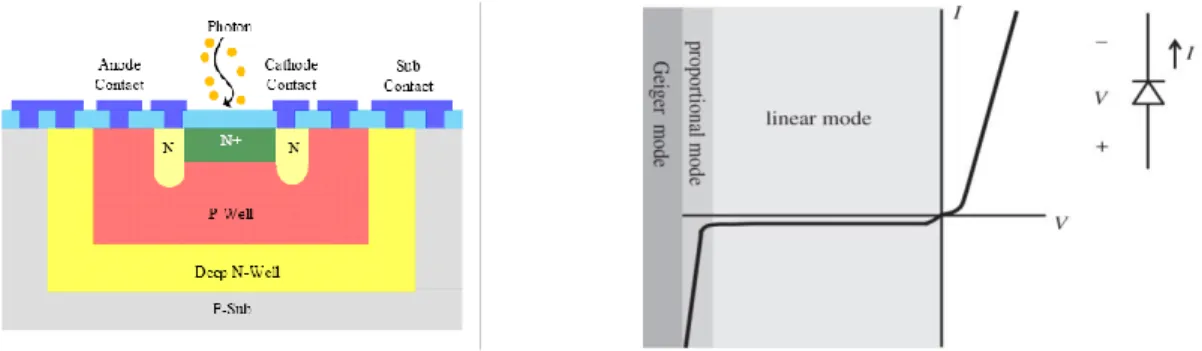
2.3.1. Photomultiplier Tube (PMT) and microchannel plates
A photomultiplier tube (PMT) is a vacuum tube consisting of an input window, a photocathode, focusing electrodes, an electron multiplier, and an anode. A PMT is based on the external photoelectric effect by which the electrons in the valence band of the material, upon absorbing the energy of the impinging photons, are emitted into the vacuum. Figure 2.2 shows the cross-section of a photomultiplier [36]. Light passes through the input window and the impinging photons excites the electrons in the photocathode. The photoelectrons emitted into the vacuum are accelerated and focussed on to the surface of the dynodes by the focussing electrodes. Considering that δ is the multiplication factor of each dynode, a PMT with n dynodes generates δn secondary electrons by means of secondary electron emission. The multiplied secondary electrons emitted by the last dynode are finally collected by the anode, which converts the electron cloud into an electrical signal. After their absorption the charges must be removed quickly from the anode surface for the prevention of surface charge effects. GaAsP photocathodes can achieve the peak quantum efficiency of 45% at a wavelength of 600 nm down to 30% at 900 nm.
Microchannel plate (MCP) PMT consists of an array of 104 – 107 miniature electron multipliers, usually fabricated from a lead glass, oriented parallel to one another and fused together to form a thin disk. The channel diameters are typically in the range of 10 to 100 µm and have length to diameter ratios between 40 and 100. An electron, which enters the channel considered as a continuous dynode structure, hits the channel wall and produces the secondary electrons which are accelerated by the electric field. The accelerated secondary electrons hit the opposite wall and make additional secondary electrons. Such microchannel plates, used singly or in a cascade, allow electron multiplication factors of 104 -107 coupled with ultra-high time resolution (< 100 ps) and spatial resolution limited only by the channel dimensions and spacings. The dark current in PMTs is the small amount of current that flows in the PMT even without the presence of any photon. The quantum efficiency and dark current increases by increasing the supply voltage of PMTs. Nowadays, PMTs are one of the technologies of choice for single-photon detection, due to their maturity and wide availability. However, the disadvantages of this technology are their fragility, bulkiness, non-portability, non-scalability, and weak spectral response in near infrared (NIR) spectral range [38] .
2.3.2. PN Photodiode
A photodiode is a reverse biased p − n junction diode, having a depleted semiconductor region with a high electric field, that produces an electric current in response to the incoming photons. When a photon of ample energy strikes the diode, it generates electron-hole pair. This phenomenon is often referred to as inner photoelectric effect. If the absorption happens near to the depletion layer, then the electrons and holes are separated and transported in the opposite directions owing to the high electric field of the junction; the holes move towards the anode and the electrons towards the cathode resulting in the generation of photocurrent. Since the electric field is very high in the depletion layer, the photocarrier generation is mostly confined to this region. Figure 2.3 shows the cross-section of a p − n junction and possible locations of electron-hole pair generation. For high-speed operation the depletion region should be thin to reduce the transit time of the photo generated carriers. However, to increase the quantum efficiency (number of generated electron-hole pairs per incident photon), the depletion region should be sufficiently thick to be able to absorb the maximum amount of incident light. Therefore, there exists a trade-off between the speed of response and quantum efficiency. Furthermore, for a given semiconductor the optical absorption coefficient, denoted by α, is strongly dependent on
Figure 2.4. Cross-sectional view of a PIN diode along with the energy band diagram, charge distribution and electric field distribution.
the wavelength, so the wavelength range for which an appreciable photocurrent can be generated is limited. The photodiode has an I-V relation as:
I
d= I
s[exp(
eV
kBT
) − 1] – I
p (2.1)The term Ip, the photocurrent, is proportional to the photon flux. Ge photodiodes, III-V ternary photodiodes (e.g., InGaAs) and III-V quaternary photodiodes (e.g., InGaAsP) have shown high quantum efficiencies.
2.3.3. PIN Photodiode
A p − i − n photodiode is a special case of p − n junction photodiode because the depletion-region thickness or the lightly doped intrinsic layer sandwiched between p and n layers can be tailored to optimize the quantum efficiency and frequency response. Figure 2.4 shows the schematic representation of the p-i-n photodiode. Light absorption in the semiconductor results in the creation of electron-hole pairs. Because of the high electric field across the junction, the pairs produced in the depletion region or within a diffusion length will eventually be separated and drift across the junction in opposite directions leading to current flow in the external circuit. Figure 2.4 illustrates the energy band diagram, charge distribution, and electric field distribution for a reverse biased p − i − n diode. Using the intrinsic region has two advantages. 1. Increased depletion width: it can be translated in increasing the photon absorption depth which means
Figure 2.5. Schematic of a quantum dot photon detector [39]
more absorption in red and IR region of light. 2. Decreased junction capacitance, thereby reducing the RC delay constant. The transit time of carriers drifting across the depletion region, and the RC time response are the main sources of the response time of photodiode detectors. The response time of p − i − n photodiodes can be as low as a few hundreds of picoseconds. It should be noted that in the case of silicon, the maximum responsivity occurs on wavelengths which are substantially shorter than the bandgap wavelength. This is due to the indirect-gap nature of silicon where the photon absorption transitions typically take place from valence to conduction band states which are above the conduction band edge.
2.3.4. Quantum dot photon detector
Recently, the quantum dot based detector have been introduced for use as single-photon detector which consists of a transistor made of different layers of gallium arsenide and aluminum gallium arsenide. One of the layers consists entirely of quantum dots, which are highly sensitive to photons, placed at just nanometers separation from each other. A photon hitting the detector releases an electron trapped in the one of the dots which is picked up by a nearby highly sensitive channel. This causes a change in the resistance of the channel which is just a few nanometers above the quantum dot layer. Figure 2.5 shows the schematic of the detector. A photon detection probability of 50-86 % has been reported for GaAs, and AlGaAs types of these quantum dot optically gated field effect transistors. It is suggested that by avoiding avalanche process which can amplify both photo generated carriers and dark carriers, quantum dot photodetectors can have lower noise. Since this type of single photon counter is based upon a transistor, it is expected that the device can scale with technology and operate at low voltages (< 5 V).
Figure 2.6. Energy band diagram of a Schottky-barrier photodiode
2.3.5. Superconducting Single Photon Detector
Single-photon detectors based on superconducting nanowires (SSPDs or SNSPDs) incorporate thin films of superconducting material shaped into meandering nanowires and have rapidly emerged as a highly promising photon-counting technology for infrared wavelengths. The superconducting single photon detectors generally use niobium-nitride (NbN) nanowires [40] as the medium of photon absorption. The resistance of the superconducting nanowire is zero, hence no voltage appears on the nanowire even in the presence of an electrical current. However, the absorption of a single photon at some point in the nanowire raises the temperature of that point, locally destroying the superconductivity. Thus, a finite resistivity appears in the nanowire which rapidly disappears as the nanowire is being cooled by the cryocooler and it turns superconducting again. This change of resistance creates a voltage pulse, clearly depicting the arrival time of a single photon at the superconducting nanowire. In general, the superconducting devices offer high quantum efficiency, low dark counts, low leakage current and excellent timing resolution but they have to be cooled to a very low temperature typically 2-4 K. The complexity and huge size of the cooling equipment limits the practical utilization of these devices.
2.3.6. Schottky barrier photodiode
Schottky barrier photodiode is simply a depletion layer photodiode in which the p-n junction is replaced by the metal-semiconductor heterojunctions. Schottky-barrier photodiode would result if the p or n type layer in the device is replaced by a thin transparent metal and is able to operate in two photo-detection modes: (i) Electron pair generation occurring from band to band or energy gap excitation in the semiconductor and (ii) Emission of carriers occurring from the


![Figure 2.18. Schematic cross section of the device with a retrograde doping profile in 180nm CMOS technology [70]](https://thumb-eu.123doks.com/thumbv2/123doknet/2346951.35118/58.893.102.793.371.574/figure-schematic-section-device-retrograde-doping-profile-technology.webp)
![Figure 2.20. Cross-section of the circular STI-bound SPAD 130nm CMOS technology [72]](https://thumb-eu.123doks.com/thumbv2/123doknet/2346951.35118/59.893.175.715.430.653/figure-cross-section-circular-bound-spad-cmos-technology.webp)
![Figure 2.24. Cross-section of the SPAD in 0.35μm CMOS technology, diameter of the active area are 10 µm-30 µm [76]](https://thumb-eu.123doks.com/thumbv2/123doknet/2346951.35118/61.893.207.715.821.1063/figure-cross-section-spad-cmos-technology-diameter-active.webp)
![Figure 2.26. p-well/deep n-well SPAD in 65/40 nm 3D IC CMOS technology [78]](https://thumb-eu.123doks.com/thumbv2/123doknet/2346951.35118/62.893.258.629.814.1107/figure-deep-spad-nm-d-ic-cmos-technology.webp)
![Figure 2.27. (a) Block diagram of the fast-gating single-photon counting module [87] which includes the detection head and the control unit provides all the timing and trigger inputs/outputs, the USB link, (b) Windowed TO-8 package assembly,](https://thumb-eu.123doks.com/thumbv2/123doknet/2346951.35118/65.893.113.776.814.1000/counting-includes-detection-control-provides-trigger-windowed-assembly.webp)