ACHIEVING LARGE STABLE VERTICAL DISPLACEMENT IN SURFACE-MICROMACHINED MICROELECTROMECHANICAL SYSTEMS (MEMS)
by
Erik R. Deutsch
B.A. Vassar College (May 1996)
M.S. Massachusetts Institute of Technology (June 1998)
Submitted to the Department Of Electrical Engineering and Computer Science in Partial Fulfillment of the Requirements for the Degree of
Doctor of Philosophy
at the Massachusetts Institute of Technology June 2002
© 2002 Massachusetts Institute of Technology
All Rights Reserved.
BA RKER MASSACHUSETTSINSTIT T OF TECHNOLOGY
JUL 3 1 2002
LIBRARIES Signature of Author ...Department of Electrical Engineering and Computer Science
7-) June I, 2002 Certified by ... .. ...
Stephen D. Senturia, Barton L. Weller Professor Department of Electrical Engineering and Computer Science Thesis Supervisor Certified by ... ... ...A...
Rajeev Ram, Associate Professor Department oftElerical Engineering and Computer Science -Thesis Supervisor
Accepted by ... ...
.. V Arthur C. Smith Department of Electrical Engineering and Computer Science Chairman, Department Committee on Graduate Students
Achieving Large Stable Vertical Displacement in
Surface-Micromachined Microelectromechanical Systems (MEMS)by
Erik R. Deutsch
Submitted to the Department Of Electrical Engineering and Computer Science in Partial Fulfillment of the Requirements for the Degree of Doctor of Philosophy
ABSTRACT
This thesis describes electrostatic actuation techniques and mechanical design features for realizing large planar analog vertical travel in an electrostatically actuated diffractive mid-infrared optical device, which is robust, both to manufacture, and against pull-in during use. This device, called the Polychromator, is fabricated by polysilicon surface-micromachining and consists of many parallel elements, each 20 microns wide and a centimeter in length. Typically, achieving such a large travel would require prohibitively large gaps and actuation voltages. In order to reduce the actuation voltage and achieve greater travel before pull-in, thinner beams are used which exploit stress stiffening. This, in turn, creates a number of stress control hazards because tensile stress in one layer can induce buckling in a lower layer. These issues have been solved with detailed attention to supports and their compliance. A multi-layer nonlinear spring has been incorporated to make the device robust against pull-in. The electromechanical behavior of the device is simulated using Energy Methods, Finite Difference Methods, and the MEMCAD software. Excellent agreement between MEMCAD simulation and experimental measurements for this structure are reported. Each detail, stress control, support structure, and pull-in, must be addressed in order to achieve the combined effects of large travel, robustness against pull-in, and optically flat beams. Controlled planar actuation over a large vertical range at low applied voltages is obtained by combining a robust electromechanical design with a manufacturable surface micromachining process. Covering a centimeter square area, the 512 grating elements achieved 3.8 microns vertical displacement at 72 Volts with a 0.5 Volt standard deviation, indicating uniform performance across the device. The development of the device has led to innovations in position control, fabrication processes, device design, and device testing.
Thesis Supervisors: Stephen D. Senturia
Weller Professor of Electrical Engineering Rajeev Ram
Associate Professor of Electrical Engineering and Computer Science Thesis Reader: Jeffrey H. Lang
Professor of Electrical Engineering and Computer Science
3
Acknowledgments
I would like to take this opportunity to thank the many individuals who have
contributed to my personal and academic growth over the past six years culminating in the completion of this thesis.
First, I would like to thank my research supervisor Professor Steve Senturia, who introduced me to and sparked my interest in MEMS. Steve has guided me through six years of graduate school and research, has driven me to excel, and has given me the opportunity to work in this field both technically and financially. I would also like to thank thesis supervisor Rajeev Ram and thesis reader Jeff Lang for reviewing the thesis and serving on my committee.
I would like to thank the past and present members of the Polychromator team at
MIT, including, Steve Senturia, Jay Bardhan, Alicia Volpicelli, Raj Sood, Srikar Vengallatore, Elmer Hung, and Mike Hopgood, at Honeywell Laboratories, Ben Hocker, Dan Youngner, David Arch, Aravind Padmanabhan, Bill Herb, Dane Larson, and Steve Swanson, at Sandia National Laboratories, Mike Butler, Mike Sinclair, Ted Plowman, Hopper Chu, and at ACLARA BioSciences, Tony Ricco. Technical discussions with the members of the Polychromator team at Honeywell and Sandia have been insightful and helpful in many ways.
The members of my research group have been influential in making this work a success. I learned a great deal about MEMS and the Polychromator project from Elmer.
My officemates, Jay, Raj, and Alicia made significant technical contributions, and
provided much needed distractions. Jay Bardhan deserves special thanks for his help taking data for the Polychromator project, taking data with the automated testing system
for this thesis, and for critically reviewing this thesis.
Several personal friends have been instrumental in my success, sanity, and enjoyment throughout the course of this thesis and the research leading to it. In particular
I would like to thank Jay, Raj, Eric, John, Cynthia, Pei-Lin, Kamini, Kai, Yu-Han,
Michelle, and Ritwik.
Finally, I would like to thank my parents John and Edna, my grandmother Maya, my sister Karin, and brother-in-law Indraneel, for their never ending love, support, and guidance throughout the path leading me to MIT and during my time here. Without them I would not be here today.
This work was sponsored, by DARPA under contract N6601-97-C-8620.
Table of Contents
C hapter 1:
Introduction...
9
1.1 Large Travel Actuators ... 10
1.2 Thesis Outline ... 14 1.3 Near-infrared Polychromator ... 14 1.3.1 Device Design... 15 1.3.2 Fabrication Process ... 16 1.3.3 Device Operation ... 17 1.4 M id-Infrared Polychromator... 19
1.5 Summ ary of W ork of This Thesis... 21
Chapter 2:
Design and Simulation...
23
2.1 M ulti-layer Nonlinear Spring Design ... 24
2.1.1 Design Parameters ... 25
2.1.2 Design Constraints ... 25
2.2 Simulation... 26
2.2.1 Energy M ethod Analysis... 27
2.2.2 Finite Difference M ethod Analysis... 31
2.2.3 Effects of Stress ... 34
2.2.4 M EM CAD Analysis... 34
2.2.5 Comparison of M odeling Techniques... 36
2.3 Design Challenges ... 37
2.3.1 Grating End Effects... 37
2.3.2 Support Compliance... 39
2.4 Summ ary ... 41
C hapter 3:
Fabrication ...
42
3.1 Fabrication Process ... 42
3.1.1 Stacked Support Process... 43
3.1.2 Lateral Support Process ... 46
3.2 Process Developm ent... 49
3.2.1 Thick Oxide Layers... 50
3.2.2 Stress Control... 52
3.2.3 M etalization and Release ... 53
3.2.4 Packaging... 53
3.3 Results of fabrication ... 54
3.4 Summ ary ... 59
Chapter 4:
Experim ental Results ...
60
4.1 Final Device Specifications ... 60
4.2 Electromechanical Testing... 60
4.3 A ctuation R esults ... . . 61
4.4 Comparison to Models ... 62
4.4.1 Stress Determination Using FDM... 62
4.4.2 MLNLS Characteristic Using MEMCAD ... 63
4.5 D evice Perform ance... 64
4.5.1 Automated Testing... 64
4.5.2 R epeatability ... . 65
4.5.3 R eliability ... . 66
4 .5 .4 U niform ity... . 66
4 .5 .5 Y ield ... . . 6 7
Chapter
5:
Discussion and Conclusions ...
69
5 .1 S calab ility ... . . 69
5.2 A pplication s ... . . 69
5.3 Future W ork ... . . 70
5.4 C onclu sion s... . 70
Appendix A: M ask Specifications ...
72
A .1 M ask L ayout ... . 72
A.2 Mask Layer Descriptions ... 73
Appendix B: Detailed Process Flws ...
75
B.1 Stacked Support Process Flow ... 75
B.2 Lateral Support Process Flow ... 76
References ... ...
77
Table of Contents
8
8
Chapter 1: Introduction
Microelectromechanical systems (MEMS) are revolutionizing the field of optics.
MEMS structures are suitably sized to interact well with light in reflective configurations
such as the Texas Instruments Digital Micromirror Device [1] or in diffractive configurations such as the Silicon Light Machines Grating Light Valve [2]. When the reflective approach is implemented, the optical system external to the MEMS device determines the motion required by the device. When the diffractive approach is implemented, the motion required by the MEMS device is typically on the order of the incident wavelength. For visible light, this corresponds to approximately one half of one micron, which is readily achievable by surface micro-machined MEMS devices.
Specially designed phase or amplitude diffraction gratings have been shown (Sinclair et. al. [3,4]) to reproduce desired infrared spectra. A polychromatic spectrum is the result of diffraction from the optical elements in a grating (Figure 1.1). The grating described in this thesis is the Polychromator, an electronically programmable MEMS diffraction grating for use in a dark-field correlation spectrometer system. The previously reported Polychromator grating [5] has been designed to generate synthetic spectra in the 3 to 5 micron wavelength range. This grating will be referred to as the near-infrared Polychromator. The grating consists of 1024 individually addressable diffractive elements, 10 im wide and 1 cm long. Diffractive elements must remain flat and their vertical positions must be controlled over an approximately 2 micron range for the device to correctly and efficiently generate synthetic spectra. This device has been fabricated and optimized for modest travel in previous work.
Broa&and Polychro Light In Spectrar out Deflectable Micivntirr Grating Ekeens -__ -_-__-_-__-_-__ -_-__-_-__-_-_-__-_-__-_-__-_- 3600 3700 3800 3900 4000 4100 4200
* sMIeJ Afkessab i f wavenumubers d)
*Amey of Drkier Xlacmodms
Figure J.J: Polychromatic spectrum as a result of diffraction from M EMS grating.
The primary goal of this thesis is to design and fabricate a Polychromator device that extends the range of optical processing into the mid-infrared spectral region (Table
1.1). This spectral region is of particular interest because the characteristic absorption
signatures of many chemicals lie within it. The challenge of this work is to push the limits of surface micromachining and electromechanical design, subject to two main constraints: low operating voltage and the requirement for large displacement. Specifically, the voltages are limited by the dielectric properties of the insulation layer used, and the displacement must be large enough to generate spectra in the 8 to 12 micron
9 Chapter 1: Introduction
wavelength range, which requires 4 to 6 microns of travel. Iterations between design and fabrication steps are essential to the successful production of a functional device.
Specification Amount Reason
Width of the elements 20 pm Sets moderate diffraction angle
Enables scalar diffraction theory
Vertical displacement 4 - 6 m Required by Fourier models Number of grating elements 512 Provides adequate resolution
Length of the elements 1.2 cm Results in a square die area
Table 1.1: Specifications for mid-infrared polychromator.
The manufacturing process must address significant challenges including the deposition and etching of thick oxide layers, stress control for structural polysilicon layers, dielectric insulation of conductors, metal adhesion, and the minimization of print-through topography. The electromechanical design is a multi-parameter, process dependent optimization to achieve pull-in protection, reduced support compliance, reduced end effects, low cross talk, minimal electrical leakage, low operating voltage, and large vertical displacement.
1.1 Large Travel Actuators
MEMS are used in a variety of fields, including optics, transportation, aerospace,
robotics, chemical systems, biotechnology, and microscopy [6]. They are built using bulk or surface micromachining processes and are typically batch fabricated, similar to devices produced in the semiconductor industry. MEMS are typically used in these fields either as sensors, which convert mechanical actions to output signals, or as actuators, which convert input signals to mechanical actions. This section discusses actuators.
An actuator transfers energy from an input stimulus form into some type of displacement or mechanical response. Electrostatic actuation entails the application of a voltage difference to two conductors, which creates a force of attraction between the conductors and causes one or both of the conductors to move. Examples of this type of actuation are the Polychromator by Hocker et. al. [5], the DMD device by Van Kessel
[7], an electrostatic microvalve by Sato et. al. [8], and adaptive optics devices by
Tuantranont et. al. [9], and Bifano et. al. [10]. Thermal actuation exploits either a difference in the coefficient of thermal expansion (serpentine micro-bridges by Judy [11] or polyimide bimorph actuators by Ataka [12]), or a temperature difference (an optical microactuator by Huja [13]), to cause bending. Piezoelectric actuation is generated by the application of an electric field across a piezoelectric crystal, ceramic, or a thin film. The converse piezoelectric effect [14] then induces a strain, which translates into a displacement (a large displacement psuedo-static actuator by Toshiyoshi [15] or a two-dimensional micro scanner by Kawabata [16]). Magnetic actuation results from the force generated by a magnetic field; the fields are generally created by passing a current through a surface coil (the actuators described by Toshiyoshi [17], Liu [18], and Houlet
[19]). Fluidic or pneumatic actuation generally refers to the use of fluid under pressure to
displace a flexible member (the balloon actuator by Kawai [20], the micro bellows by
10
Yang [21], or the osmotic actuator by Su [22]). Conversion between different types of displacement may be achieved by cascading different types of actuators, such as the flip-up sliding plate actuator by Lee [23].
Actuators can be categorized according to the type of displacement generated. Vertical displacement describes motion perpendicular to the substrate (a diffraction grating by Hocker [5], adaptive optics devices by Tuantranont [9], and Bifano [10], or a large resonant displacement mirror by Bhalotra [24]). Lateral displacement describes motion parallel to the substrate (a scratch drive actuator by Akiyama [25], a linear inchworm motor by Yeh [26], or a diffractive varying period diffraction grating by Chen
[27]). Rotational motion refers to displacement about an axis, such as that generated in a
micromotor (Epstein et. al. [28]). Angular displacement describes tilting [7,8]; or flip-up, (micro-XYZ stages by Fan [29] or Lin [30], a raster scanned full motion video system by Conant et. al. [31], or an automated flip-up assembly system by Reid [32]); or bending motion (switching by stress-induced bending by Chen [33]).
No fundamental limitations prevent the use of any of the above actuation methods to obtain any one of the listed types of displacement. Furthermore, large travel can be obtained for almost any combination of actuation method and displacement produced, especially if the displacement is achieved by converting one type of displacement to another, for example, using leverage. The desired application dictates the final type of displacement required, and the operational specifications (both internal and external) for the device dictate the actuation method and degree of travel.
Each actuation method has its strengths and weaknesses for different types of applications. In addition to the desired magnitude of the displacement, important metrics include speed, stability, size, and ease of fabrication. Electrostatic actuators can be very fast, stable, readily integrated with existing fabrication technology, and designed to generate various types of displacement. Thermal actuators are limited in vertical or lateral displacement, but generate large forces, so are more suited to cause bending displacement. Piezoelectric actuators generally displace by a small amount, and so they are better used to generate bending rather then vertical displacement; larger vertical travel using piezoelectric actuation typically requires excessively complicated fabrication processes or large voltages, since the displacement scales with the voltage and size of the device. Magnetic actuators often require large die area since they require coils. Fluidic actuators are typically large and relatively slow. This work focuses on actuation methods for optical applications, and this considerably restricts the set of feasible choices for actuation methods.
For optical applications there are four main types of actuators: flip-up, torsion, planar vertical, and lateral. Flip-up mirrors are used for optical benches (Lin [30], Figure 1.2a) and lateral displacement actuators are typically converted to large scale motion out of plane (Conant [31]) or large-scale planar vertical travel devices (Fan [29], Figure
1.2b). These devices enable large displacement but are not scalable into a closely packed
array structure. Torsion mirrors are used to process light in reflective applications (optical add-drop switching by Ford [34] for instance) or in displays (such as the TI DMD device [7], Figure 1.3) which is particularly suited to closely spaced arrays and where light is routed depending on the mirror orientation. Vertical planar displacement of small elements allows diffractive applications (displays such as the GLV [35] or adaptive optics [9,10] for example). Lateral displacement actuators can be used to build
devices such as varying period diffraction gratings (demonstrated by Chen [27]). For reflective configurations, the type of motion of the mirrors affects the choice and size of external optics needed to collect the light; for diffractive configurations, the period of the grating and the wavelength of the incident light affect the size of the external optics, and the wavelength of the light dictates the motion required of the actuators.
(a) (b)
Figure 1.2: (a) Micro optical bench [30]. (b) MicroactuatedXYZ-stage [29].
Figure 1.3: Texas Instruments DMD device (www.ti.com)
The Polychromator device discussed in this thesis must be robust, stable, and fast. Several hundred very narrow, long, closely spaced actuators must remain flat and parallel, while moving vertically relative to the substrate surface and operating at reasonable voltages. These device requirements significantly constrain the device structure and limit the choice of actuation method.
The motivation for choosing an electrostatic actuator for the near-infrared Polychromator is discussed in depth by Hung [36]. The near-infrared Polychromator structure consists of a bending beam below a flat beam and segmented electrodes, exploiting a method called leveraged bending. A simple extension of this design to obtain larger vertical displacement would require larger gaps to enable sufficient travel before the electromechanical pull-in instability. This increase in gap would, however, significantly increase the required operating voltage. Two methods to reduce the operating voltage are to use thinner beams to reduce the elastic restoring force of the beam, and a continuous electrode to increase the electrostatic force between the beam and an underlying electrode.
Chapter 1: Introduction
12 12
Another method to reduce voltage is to use shaped electrodes. This technique, described by Wagner [37], uses gray-scale lithography to etch a sloped surface, or gradual electroplating to build up a sloped surface. The sloped surface can be formed to be closer to the actuated element, thereby decreasing the operating voltage. The main drawbacks behind this approach are that the sloped surface must be planarized, the sloped surfaces are difficult to fabricate, and the sloped electrodes can take up significant area.
As noted above, Hung [36] discusses a method to increase travel using the leveraged-bending concept, which extends the range of displacement past the electromechanical instability, by using segmented electrodes positioned nearer to the supports than to the midpoint of a beam segment. The leveraged bending design increases the vertical displacement at the expense of increasing the actuation voltage. For the desired displacement in the mid-infrared Polychromator, the leveraged bending design would correspond to a prohibitively large operating voltage range. Bums [38] discusses a nonlinear flexure design in which a main cantilevered flexure contacts an auxiliary doubly supported element, which increases the stiffness and travel of the device. This design increases the vertical displacement at the expense of increased actuation voltages. Implementing the design would entail additional process complexity, such as additional polysilicon and oxide layers, if it were to enable the desired displacement for the mid-infrared Polychromator.
The two-tiered beam concept (the lower beam bends and the upper beam remains flat) is very versatile, and a variety of other actuation methods (piezoelectric, thermal, or magnetic), can be used to cause the lower beam to bend. Kawabata [16] describes a micro-scanner in which an integrated piezoelectric thin film bends a mirror out of plane. This actuation principle could be used to bend the lower beam and cause vertical motion (up or down) of the center of the beam element. An actuator based on this principle does not become unstable like an electrostatic actuator so vertical dimensions would be less and the device could travel the entire gap. Fabrication of the piezoelectric elements with additional polysilicon processing, however, would add significant process complexity.
Tuantranont [9] describes a bulk micromachined piston type mirror with a 2 to 3.5 micron vertical displacement capability, designed for adaptive optics. The square device is suspended by thermal multimorph flexures at each corner, which curl due to ohmic heating of multilayer films, each of which has a different coefficient of thermal expansion. A linear actuator could also be designed using this actuation principle. Thermal multimorph flexures would be used to bend the lower beam of the two-tiered structure. Both actuation methods, while feasible, would considerably complicate fabrication, be difficult to achieve the desired packing density, and would lack the microsecond speed of an electrostatic actuator.
Liu [18] describes a magnetic actuator designed such that a surface micromachined coil causes the bending of a plate that is connected to the substrate by cantilever beams. This technique can be used to cause bending or vertical motion directly. The coil in this work is fabricated on the moving plate, but could be fabricated on the substrate. This magnetic coil, if integrated with a lower bending beam and a flat upper beam, could provide the necessary vertical displacement, but the coil size would limit the lateral dimensions of the grating elements. In addition, the magnetic coils would complicate fabrication and introduce topography for the upper layers.
Chapter I. Introduction
13
1 3 Chapter 1: Introduction
Electrostatic actuation comes closest to fitting the combination of desired features for the mid-infrared Polychromator, without significant fabrication complexity, and was therefore chosen as the method to achieve large vertical travel.
1.2 Thesis Outline
This section provides an overview of the material discussed in this work. In the present chapter, previous work on the near-infrared Polychromator device is presented as background for the work presented in the thesis. The motivations for extending the range of operation of a programmable diffraction grating from its initial configuration in the 3 to 5 micron wavelength range, to operate in the 8 to 12 micron wavelength range and the
device specifications are described. Finally, the work done for this thesis is summarized.
Chapter 2 presents the parameters and constraints affecting device design and the simulations used to demonstrate the functionality of the device. A simplified but
illustrative energy method model, a more accurate idealized finite difference method (FDM) model, and a more detailed structurally exact model are used to simulate device designs and predict performance. Two design challenges that were overcome in this
work, end effects and support compliance, are addressed, and the discussion highlights
the interaction between design and fabrication.
The fabrication of the device is discussed in Chapter 3, encompassing device layout and the process flow, and is illustrated using device cross-sections. The development of key process steps to build tall structures is also discussed. Fabrication challenges including metalization, release, and packaging are addressed. The results of the fabrication process are then presented.
The experimental results of this thesis are presented in Chapter 4. The method of experimental testing of displacement is described. Beam displacement characteristics for several fabricated designs are measured, and the designs are then compared to models to estimate the stress in the devices. The results are compared to full simulations based on the extracted stress, and show excellent agreement. The measurement repeatability of a single element, the reliability over many actuated cycles, the uniformity of actuator performance across the device, and the device yield is reported using data collected by an automated measurement system.
Chapter 5 describes the scalability of the design and concludes with a brief
discussion of the work presented in the thesis and future work that could be based on this device.
1.3 Near-infrared Polychromator
The Polychromator project is a collaboration between the Massachusetts Institute of Technology, Sandia National Laboratories, and Honeywell Laboratories. The spectral synthesis, optical system fabrication, and experiments to demonstrate gas detection were performed at Sandia Labs. The majority of the fabrication and process development was performed at Honeywell Labs. Electromechanical design, simulation, part of the fabrication and process development, and testing was performed at MIT.
14
The near-infrared Polychromator diffraction grating, discussed as background for this thesis, was designed to process light in the 3 to 5 micron spectral window. The elements of the diffraction grating were designed to achieve 1.5 to 2 microns of planar vertical travel in a low tensile stress polysilicon surface-micromachining process. The design includes several notable design features such as leveraged bending and a two-layer beam structure, and is capable of actuation to almost the full gap with planar vertical displacement. The fabrication of the device employs a custom, 11 mask fabrication sequence, which does not significantly differ from currently available standard fabrication processes. The fabricated structures exhibited the desired actuation and optical characteristics.
1.3.1 Device Design
The deflection of each element is a function of the applied voltage, and the maximum travel is limited by an electromechanical instability called pull-in [39]. Stable displacement is maintained upon increasing voltage until pull-in; at pull-in, the beam snaps to the underlying electrode, after which the system no longer has a point of stable equilibrium, and in most cases is a critical device failure. For the beam lengths and widths used in this design, and for a beam thickness comparable to the free-space gap, actuation via a continuous underlying electrode results in pull-in when the lower beam is displaced by approximately one-third of the free-space gap. To achieve positioning beyond the pull-in instability, the design of the Polychromator device takes advantage of leveraged bending [40]. The grating element design shown in Figure 1.4 and Figure 1.5 uses a two-beam structure attached periodically to the underlying layer, in which the lower beam undergoes bending while the top mirror beam deflects vertically without flexion.
Applying voltage to the segmented actuation electrodes located near the support posts allows leveraged bending of the lower beam and controllable positioning of the upper mirror beam through the full gap. Electromechanical analysis tools are used to help design structures capable of near-full-gap actuation with voltages of about 100 volts or less. The gaps and beam thicknesses are about 2 pm. For the near-infrared devices, post-to-post spacings (B) are in the range of 500 to 700 pm, and electrode lengths (E) are in the range of 80 to 100 pm.
G
Repeated Repeated
Structure Structure
Figure 1.4: View of the unactuated Polychromator grating beam structure in cross-section (B is the doubly-supported beam length, E is the length of one segmented actuating electrode, L is the ground pad length, and G is the
lower and upper free-space gap).
Chapter 1: Introduction
15 15
Repeated ~L~Repeated
Structure Structure
V GND
Figure 1.5: View of beam structure in cross-section when actuated. The lower beam undergoes bending, while the top mirror beam remains flat and deflects vertically (D is the vertical displacement from the original position when voltage V is applied to the actuating electrodes).
1.3.2 Fabrication Process
The near-infrared Polychromator grating device is a combined Honeywell-MIT fabrication effort, using polysilicon surface micromachining. Two polysilicon layers are used to create the actuated structure, and two more are used for electrical interconnections and actuating electrodes. The process begins with growth of a thermal oxide on an ultra-flat silicon wafer. Two layers of boron-doped polysilicon, separated by silicon nitride, are used for the interconnection and electrode structures. Next, a sacrificial silicon dioxide (SiO2, or simply oxide) layer is deposited, which will define the actuation gap. Support posts for the bending layer of polysilicon are patterned and etched in this oxide layer. Before the deposition of the bending layer of polysilicon, small dimples are also etched in the oxide. The dimples cause nodules to form on the bottom of the polysilicon layer; these nodules help prevent stiction during operation, should the bending beam pull in. The bending layer of polysilicon is then deposited, implanted, and patterned, and the second sacrificial oxide layer is deposited. The second oxide layer has vias etched in it to create support posts for the polysilicon mirror beam layer. The polysilicon mirror-beam layer is then deposited, implanted and patterned. Typical thicknesses for the bending and mirror beam layers of polysilicon and for the two sacrificial oxide layers are approximately 2 pm. The wafers are then annealed to reduce the polysilicon stress. The process is completed with the deposition of gold onto the mirrors and pads and the removal of all of the sacrificial oxide. The fabricated element and grating are shown in Figure 1.6 and Figure 1.7.
Chapter 1. Introduction
16
16 Chapter 1: Introduction
Figure 1. 6: SEM ofgrating showing the double beam, support structure, interconnects,
and electrodes [5].
Figure 1.7: SEM of the edge of a MEMS Polychromator grating showing
interconnects, lower bending beam, and upper mirror beam. Beams are 10 microns wide and 1 centimeter in length [5].
1.3.3 Device Operation
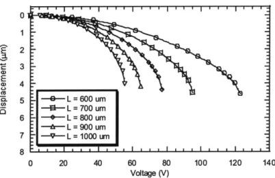
The individual diffractive elements of the Polychromator grating are actuated electrostatically. Beam deflection depends primarily on the applied voltage, electrode length, distance between support posts, beam thickness, residual stress, and free-space gap. Combinations of mask design and process parameters are selected to result in structures that maximize travel while requiring only moderate actuation voltage. To evaluate fabricated devices, interference microscopy is used to measure vertical movement of individual beam elements as a function of applied voltage, such as by Volpicelli [41] or by Bardhan [42]. Results for several grating element designs are shown in Figure 1.8. Measured maximum beam deflections for these devices are nearly the full gap of two microns, and pull-in occurs at voltages ranging from 65 to 110 volts, depending on the particular device design.
Chapter 1: Introduction
17
17 Chapter 1: Introduction
I - - - - -=-=--- -0 Z~ 0.5 E 1.5 00/100 nnIn500(90 s 2 . . . I . . . . . . . 100/100 . 500/- - 50 /810 0 20 40 60 80 100 120 Applied Voltage (V)
Figure 1.8: Displacement versus actuating voltage for a variety of grating element designs (numbers in the figure indicate the beam length to electrode length
relationship B/E in Figure 1.4 in microns for each design) [5].
To minimize packaging complexity, the first devices fabricated used only 132 pads for signal and ground; this decision allowed integration with a readily available pin-grid-array package (Figure 1.9). In order to actuate all 1024 lines with this limited input/output capability, the grating elements are hard-wired on-chip as 8 repeat units of
128 elements. In this configuration, a voltage applied to a bond pad actuates 8 grating
elements, one from each repeat unit. This on-chip hard wiring, while advantageous for device packaging and initial testing, has a deleterious effect on device yield; if any one of the eight lines connected to a pad is compromised, none of the eight elements in that set will function. Despite the drawbacks of this configuration, successful synthetic spectra have been demonstrated (Figure 1.10) and optical results have been obtained (Figure 1.11) [5].
Figure 1.9: Packaged Polychromator die. Array is 1 cm x 1 cm [5].
18 Chapter 1: Introduction
2000 2100 2200 2300 2400 2500 2600 2700 2800 2900 3000
Wavenumber (cm-1)
Figure 1.10: Spectral transmission of the near-infrared Polychromator for the two grating profiles used for CO2 detection. The solid line spectrum matches
the CO2 absorption at 2350 cm', while the double-bandpass dashed line spectrum samples an equal area outside the CO2 absorption [5].
IM
60 100 140 180 220 260 300 340
Tint (seconds)
Figure 1.11: Response of the correlation spectrometer to 100 ppm-meters of CO2
admitted and purgedfrom a gas cell 3 times [5].
1.4 Mid-Infrared Polychromator
The mid-infrared Polychromator diffraction grating is designed to process light in the 8 to 12 micron spectral window. Processing light in this wavelength range requires altering several features from the previous near-infrared design, including the beam width, the target vertical displacement, and the number of elements. Other features, such as the length of the elements, and the space between elements, remain essentially unchanged. The design choices are outlined in this section and the resulting specifications for the device are presented.
The overall optical system is governed by the diffraction angle of the device. The larger the diffraction angle can be set, the more compact the optics are and the easier it is to put the optics around the device. The diffraction angle of the grating is set by the diffraction grating formula, 0 = sin' ( d), where A is the wavelength of interest and d is the minimum period of the grating. The minimum period of the grating occurs when
every other beam is displaced and is thus twice the pitch of the grating. In order to effectively diffract light at one observation angle and create spectra in the region of interest, it is necessary to set the diffraction angle smaller than the diffraction angle for the smallest wavelength. The width of the beams directly affects the diffraction angle; the wider the grating elements are, the smaller the diffraction angle will be.
The algorithms designed by Sinclair et al. [4] to reproduce the desired spectra are based on scalar diffraction theory. In order for these models to be valid (so that analysis may avoid the use of vector diffraction theory, which would be significantly more computationally intensive) the beam widths should be wider then the longest wavelength of interest. In order to satisfy the constraints on diffraction angle and diffraction theory the width of the elements were chosen to be 20 microns.
The models used by Sinclair to generate the synthetic spectra use Fourier analysis to determine the vertical position of the diffractive elements. The analysis requires that, for optimal spectra, the beam be capable of sufficient displacement to induce a phase shift of 2n. For this phase shift (corresponding to a vertical beam displacement of 2)
the desired wavelength range necessitates 4 to 6 microns of planar vertical travel. It is possible to generate spectra with less travel, but the resolution and efficiency of the grating will be degraded. The reproduced spectra may have the wrong relative intensities of the features in the desired spectrum, as well as washed out spectral features of the desired spectra, as the maximum achievable displacement is decreased.
The number of beams directly affects the resolution of the device, which is the ability to resolve or reproduce a desired spectral feature. The resolution is given by:
Y2 , which scales directly as: #Beams. Therefore, as the number of beams on a
device decreases, the spectral resolution decreases proportionally. For the spectra of interest in the mid-infrared region, a resolution of about 250 is sufficient, so the number of elements was chosen to be 512.
The main factor determining the optical efficiency of the grating is the ratio between the width of the grating element and the space between elements. As this ratio increases, the grating becomes increasingly efficient, because more light is diffracted and less light is lost, or scattered, by the spaces. Therefore, increasing the elements' widths or decreasing the space between elements increases the efficiency of the grating. The minimum space is limited by the available process technology minimum feature size of two microns for the mirror layer.
The length of the elements may be chosen somewhat arbitrarily. The decision for the element length is based on keeping the optics relatively simple by having a square optical area. The length of the elements, without using cylindrical optics, is equal to the width of the device. The lengths of the elements are thus the pitch of the elements multiplied by the number of elements, and the pitch of the grating is defined to be the
width of one element plus the space next to it.
In order to operate in the wavelength range of interest and successfully build devices given the complexity of achieving the desired travel, devices that achieve between 4 and 6 microns of travel are designed. The fabrication technology used has a minimum feature size of two microns, and the space between grating elements is set to this size, to maximize diffraction efficiency. The widths of the elements are chosen to be 20 microns so that the diffraction angle of the device is not too small and the optical
20
theory is within the scalar diffraction limits. By using 512 elements and a pitch of 22 microns, the width of the device is 1.1 centimeters; this also then determines the length of the elements. The minimum first order diffraction angle with a period of 44 microns is just over 10 degrees, which does not overly complicate the optics external to the device. It should be noted that none of these parameters is independently essential to the device performance; rather, it is the combination of parameter choices that results in effective device performance.
1.5 Summary of Work of This Thesis
The mid-infrared design created for this thesis was based largely on the near-infrared design described above. The design process focused on meeting the new specifications, while implementing design and process simplification, and improving manufacturability. The process complexity was reduced by using three layers of polysilicon instead of four, as in the previous design. A nitride spacer, used as a critical insulator in the near-infrared design, was not robust to manufacturing; it was therefore subsequently designed out of the process by redesigning the beam support structure, highlighting one of the focuses of the thesis - the mutual dependence between structure design and fabrication sequence.
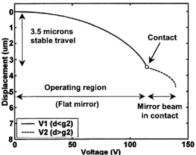
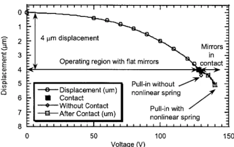
In Hung [36], the nonlinear spring effect was demonstrated in the near-infrared leveraged bending prototype structure. The fabrication process of these devices limited the upper gap to 0.6 microns, at which point the upper beam contacts the lower support posts. As voltage is increased, the experimental results of the stiffer two-beam structure deviate from simulations, which predict nearly full travel of the lower beam segment (Figure 1.12). The configuration did not allow full voltage-displacement testing of the prototype device. This limitation was turned into a critical enabling feature of the current design, and is called the multi-layer nonlinear spring (MLNLS) (Section 2.1). Hung suggested using the stress-stiffening concept to achieve large travel [36]; simulations of devices exploiting stress stiffening were used to explore the design space, and indeed, a design window that could exploit this concept was identified and used here. Several designs that met the goals of large displacement in simulation were fabricated and tested.
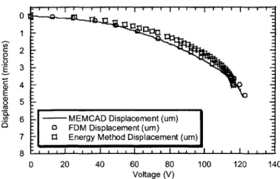
Initial modeling of the multi-layer nonlinear spring concept was performed using an energy method analysis (Section 2.2.1), which balances the stored energy in the displaced beams with an electrostatic force. This technique allowed rapid exploration of the design space by using analytical expressions for the relation between design variables and performance metrics. Since this was a very approximate calculation, more exact simulations were conducted with two focuses: displacement characteristics, and pull-in protection. The displacement design space was mapped as a function of the most significant design and process variables (beam length and free-space gap) using a modified version of FDM code from previous work by Hung [36] (Section 2.2.2). The pull-in protection was simulated using the MEMCAD 4.8 software [43] (Section 2.2.4). An ideal beam was also modeled using MEMCAD to validate the FDM simulations (Section 2.2.5). Deleterious end effects encountered in the near-infrared design were analyzed, and eliminated using tethers to compensate for stress imbalances (Section
Chapter J. Introduction
21
2.3.1). Careful consideration was given to support design, given the height of the supports and the stress in the polysilicon (Section 2.3.2).
0 0.2 -' 0.4 -S 0.6 0.8 -1 -Contact 1.2 -S1.4
1.6 - Simulation (no contact)
-1.8 Experiment (contact) X
2 7
0 20 40 60 80 100
Voltage (V)
Figure 1.12: Plot of displacement versus voltage for prototype near-infrared device using a limited process such that the upper beam segment only moved down 0.6 microns before contact [36].
Two fabrication processes were developed in collaboration with the Honeywell team to enable large travel; the first (Section 3.1.1) suffered from fabrication difficulties, but the second (Section 3.1.2) succeeded in producing functional devices (Section 3.3).
A robust thick oxide deposition strategy was developed that enabled the fabrication of the
large gaps necessary for the design (Section 3.2.1). Effectively, a fabrication process was developed around a design concept, and then the fabrication process suggested a new design concept, which simplified the fabrication process.
The completed structures are tested using an interference microscopy-based testing system, set up by Bardhan [42] (Section 4.5.1), by imaging optical fringes on a tilted sample. This can be used to map a fringe shift to a vertical displacement, as voltage is applied to a diffractive element. Experimental results from different devices on the same wafer enabled the estimation of the residual stress; the consistency of the estimated stress value from devices with varying beam lengths validated both the models and the experimental results (Section 4.4.1). The full experimental device behavior showed excellent agreement to the simulation of the full device structure as modeled using the
MEMCAD software (Section 4.4.2). The automated system enabled determination of
repeatability, reliability, uniformity, and yield (Sections 4.5.2-4.5.5). Successful devices are now being incorporated into bench-top Polychromator systems for spectroscopic evaluation by the sponsoring agency.
Chapter 1: Introduction
22
Chapter 2: Design and Simulation
This chapter describes the design of the mid-infrared Polychromator and the simulations used to model the design. In order to generate synthetic spectra in the 8 to 12 micron wavelength region the diffractive elements should travel approximately 6 microns. If the leveraged bending near-infrared design were simply scaled up to allow 6 microns of displacement, the required actuation voltage would be prohibitively large (in the range of several hundreds of volts). If the beam lengths are increased significantly to reduce actuation voltage, the yield could deteriorate due to process difficulties such as buckling or stiction. However, if a single electrode is used under a doubly supported beam and the thickness of the beam is decreased as the gap is increased, the beam enters a regime of stretching rather than bending [40]. Stress stiffening increases the achievable travel from one-third of the gap to just over half of the gap. This simple doubly supported beam design (Figure 2.1) is, however, susceptible to pull-in unless the travel is limited. In the MLNLS design, the upper mirror beam is used to stiffen the lower actuating beam (Figure 2.2), increasing the pull-in voltage and travel of the two-beam combination and thus performing this limiting function. This multi-layer nonlinear spring (MLNLS) design is introduced, and design parameters (Section 2.1.1) and constraints (Section 2.1.2) that limit the design are discussed.
Metal-1
Oxide-3 92 2
Nitride-2 Oxide-2 91
Figure 2.1: Polychromator beam structure in cross-section for the unactuated state
(g, is the lower gap and g2 is the upper gap, t, is the actuating beam thickness and t2 is the mirror beam thickness).
Figure 2.2: Beam structure in the actuated state. The lower beam segment of length, L, undergoes bending, while the top mirror beam remains flat and deflects vertically, distance D, when voltage is applied to the actuating electrode. Chapter--- 2:-Thery-andSimulaions-2
23
Several methods for modeling Polychromator designs were used for different purposes and each is presented here. Energy method analysis (Section 2.2.1) provides an analytical model of the device behavior and allows rapid insight into the design space. Finite difference method (FDM) simulations (Section 2.2.2) are then used to more accurately determine lower beam travel and actuation voltage. From FDM simulations, a set of designs can be found to span the design space that meets the constraints of fabrication and actuation voltage. The MEMCAD software (Section 2.2.4) is used for full 3-D electromechanical simulations of the set of designs, using contact boundary conditions and more exact structural geometry, and thus provide more accurate modeling tools of critical design features. Experimental results can be compared to the MEMCAD simulations, so that device performance can be quantifiably analyzed against computational predictions.
End effects in the grating elements were observed in the near-infrared Polychromator that caused pull-in prematurely (at a lower travel than predicted). A model of the shape of the end of an element matched experimental results. New designs were created to avoid this problem and then simulated to ensure that the effect had been eliminated. The new design, once fabricated, did not suffer from the previously observed failure mode. This is a good example of the interaction of the design and fabrication processes required to realize the device. Support compliance was known to be a problem in the near-infrared devices, and was expected to have even more significant effects in the mid-infrared devices because the supports are taller. To understand support compliance effects, a significant quantity of modeling was done prior to fabrication of the mid-infrared devices. Supports were designed to be robust by balancing the stress being applied to them.
2.1 Multi-layer Nonlinear Spring Design
The operation of this device is similar to the near-infrared device: a lower bending beam, which is attracted to a lower layer by an electrostatic field, displaces a flat beam vertically. The process has been modified so that only three layers of polysilicon are required (Figure 2.1 and Figure 2.2). Replacing the interconnect and electrode layers from the near-infrared design with one layer that provides both functions reduces the complexity of the design, and eliminates the electrical shorting behavior between the layers observed in crossovers required in earlier designs. Isolation between the electrodes and beam posts is created by adding insulating nitride at the supports (as in Figure 2.1) or by having segmented or lateral supports (Figure 2.24b and Section 3.1.2) so that the electrode can continue beneath it. When the nitride insulation is used, the supports and nitride insulation are recessed (Section 3.1.1) to minimize topography in the beams and mirror layers. Several key design parameters in both layout and process must be chosen, subject to design constraints, to enable the desired displacement.
Chapter 2: Theory and Simulations
24 24
2.1.1 Design Parameters
In order to achieve the desired upper beam actuation, several parameters must be chosen in the layout and process: beam segment length, electrical isolation method, and film thickness (Figure 2.1). The beam length is the most important factor in choosing the layout parameters. As beam segment length increases, the pull-in voltage decreases, and fabricating functional devices becomes more difficult due to processing problems such as stiction during release. There is also a slight decrease in the stable vertical travel (prior to pull-in) of the beam for longer beam lengths.
Electrical leakage or cross-talk between adjacent electrodes can occur when applying high voltages to the device. To try to prevent these effects, a grounded spacer in the electrode layer that runs between the electrodes, as well as a larger space between electrodes, were included in some designs. These features had not been included in the near-infrared Polychromator, so some mid-infrared designs included this feature to test the effect of this modification. The decreased width of the electrodes increases the
pull-in voltage but can prevent electrical device failure.
Given a beam segment length, the thickness of the deposited films determines the functionality of the device. Actuation voltage and total displacement before pull-in are determined by the choice of the lower gap g, and the actuation beam thickness t1 (Figure
2.1). If the lower gap is increased, a larger voltage is necessary to actuate the beam to a
given displacement, and the maximum travel is increased. If the lower beam thickness is increased, the beam will have a higher pull-in voltage at a marginally decreased maximum displacement. The upper gap g2 and the mirror beam thickness t2 are designed
to limit the travel of the lower beam by permitting the upper beam to contact the supports of the lower beam. This contact - designed to occur before the pull-in instability point of the lower beam alone - creates a stiffer two-beam structure that requires more voltage to displace it beyond the "touchdown" displacement than if the lower beam were actuated alone. This nonlinear spring effect prevents catastrophic pull-in, shorting, and possible device failure, by increasing the stability of a non-stiffened beam before it becomes unstable. The upper gap must be less than the stable displacement of the lower beam, so that the lower beam is stiffened before the pull-in instability is reached. To maximize travel and pull-in protection, the upper gap should be 70 to 90 percent of the expected travel before pull-in, which corresponds to an upper gap thickness that is about half of the lower gap thickness. The mirror beam thickness determines the stiffness of the two beams after contact. The thicker the mirror beam is designed, the stiffer the new spring becomes, requiring a larger voltage before the two beams eventually reach pull-in. However, as explained in Section 2.3.1, a thicker upper beam aggravates an end-effect which required redesign to permit stable operation while maintaining flatness across the
optically accessed section of the device.
2.1.2 Design Constraints
There are three main constraints on the design: the available voltage range, the mask requirements, and the process technology. The dielectric properties of the thin films used in the fabrication of the device, such as dielectric constant, breakdown voltage,
surface leakage, and dielectric film quality, effectively limit the voltage range to below
130 Volts. The type of electronics used also limits the voltage range. For the
near-infrared Polychromator a 128-channel voltage source with a 0 to 200 Volt range was developed [44]. For bench top demonstration systems a 512-channel 150 Volt voltage source was developed. For eventual integration into an ASIC voltage driver, designs with less than 80 Volts actuation are desired. The constraints on the mask design include the minimum feature size (two microns), the size of the desired active optical area (approximately one square centimeter), and the interconnects and bond pads necessary to apply voltages to the chip. The process technology constrains the thickness of each layer.
A thin layer (less than one micron) may not be mechanically robust enough to function
correctly, but a thick layer (poly more than 2-3 microns, and oxide more than 4-5
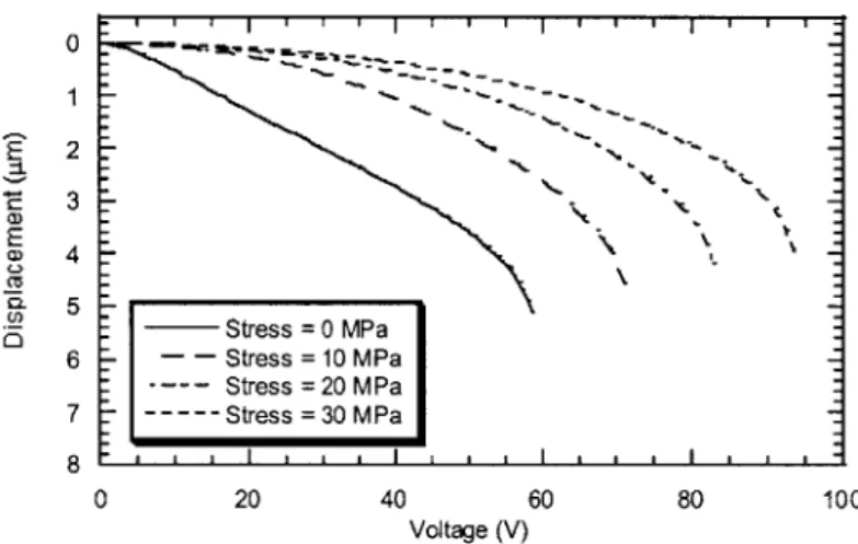
microns) is more difficult to fabricate since thick films are prone to cracking. A thick layer is also more difficult to pattern and etch. Achieving the desired geometric properties is also more difficult. The film stress is one of the most important factors in processing. If a film is compressive, the beams will buckle and be mechanically useless. For tensile stress, as the residual film stress in the beam increases, the actuation voltage required for a specific beam displacement increases and the displacement at pull-in decreases. In order to maximize travel and minimize voltage, it is desirable to have a very slightly tensile film stress, in the range of 5 to 15 MPa.
In order to achieve six microns of travel the lower gap must be approximately 12 microns. This is very aggressive for a surface micromachined process, and so process variations with various thicknesses were fabricated in the initial processing run to validate the voltage-displacement models and the MLNLS effect, and to push the limits of fabrication. The designs have lower gap thicknesses of 6, 8, 10, or 12 microns. The beam thickness was chosen to be 1 micron for all designs. As explained in Section 2.3.2, if beams are thinner than 1 micron, the supports will not be structurally rigid. If beams are thicker than 1 micron, the actuation voltage will be too high. The upper beam was chosen to be at least two microns thick, but could be thicker if fabrication allowed. In order to test several designs for a range of processing conditions, the mask contains a set of designs with different beam segment lengths. These range from 600 to 1200 microns: below 600 microns, the actuation voltage would be too high, and above 1200 microns, beams would not be mechanically reliable. Given these bounds on the design parameters, it was necessary to find a parameter space that would perform within the given constraints. The role of simulation was to help find a reasonably tight bound on the parameter space in which devices would perform to the desired specifications.
2.2
Simulation
Three types of simulations are used to describe and analyze the multi-layer nonlinear spring (MLNLS) design. Energy method analysis allows rapid insight into the design space by providing an estimate of the device functionality. Finite difference methods (FDM) allow more accurate modeling and are used to characterize the displacement of the lower beam as a function of beam segment length and free-space gap for an ideal doubly supported beam; FDM analysis is also used to investigate the effects of stress on the design. MEMCAD simulations provide the most accurate modeling of the techniques and are used to simulate the full two-tiered beam structure - in particular,
the critical MLNLS design feature, exact structural geometry, and non-ideal boundary conditions. The three modeling techniques are compared using an ideal structure to quantify the differences between each simulation tool and validate the use of FDM simulations for device design.
2.2.1 Energy Method Analysis
MEMS devices are well suited to energy method analysis since the systems
conserve energy [45]. In equilibrium, the energy stored in the system will equal the work done to the system. In an analysis of a doubly supported beam with an underlying electrode, the stored energy arises from the bending and stretching of the beam under a uniform load. The work done by the external load is the force of attraction multiplied by the change in displacement between the beam and electrode. In energy method analysis a trial function is chosen to represent the shape of the deflected beam. Depending on the residual stress in the beam, a cosine or exponential estimates the shape accurately enough to get meaningful results for several microns of displacement; beyond this threshold, the approximated beam shape no longer accurately models the deformed beam.
In the following description a cosine beam-shape trial function is used (Eqn. 1). The beam segment length is L, the center displacement is d, and v(x) is the amount of vertical displacement of the beam at each position x on the beam (Figure 2.3). The beam is centered at zero and the ends are fixed at ± .
V() d. ~ 2 -;T -x
vI) -- 1+ cos II(1)
2 ( L
Figure 2.3: Cross-section of beam-shape and reference point for a model of an ideal doubly supported beam.
Once the total axial strain from bending and stretching of the beam is integrated over the entire beam, the total strain energy and the potential energy in the system can be found. Differentiating the expression for the potential energy with respect to the displacement, setting the result to zero, and solving gives an expression for the load on the beam as a function of its center deflection [45]. In the two-beam structure the bottom beam experiences an approximately uniform distributed pressure load, q, over the entire beam resulting from an electrostatic force between the beam and the underlying electrode (Eqn. 2) (Figure 2.4a). The top beam at contact experiences a point pressure load, P, in the center of the beam where the two beams are connected (Eqn. 3) (Figure 2.4b). For an extra change of displacement after contact, more elastic energy is stored in the beam structure, since the mirror beam is bending also; equivalently, the structure is a stiffer
27
spring. In the following equations, E is the Young's modulus of polysilicon, O is the axial residual stress, t1 and t2 are the thicknesses of the lower and upper beam, and g2 is the height of the upper gap.
U0 -ti,-72 E-ti .7 E-t,-x * r
q= 2 -d+ - 3 4 -t -d + 4 -L4 d (2) L23-L 4 4-L4 U t2 *W 7r 2 (d g2 +E E 2 t| W 7 4 (d g2 +E-t2'W'r (d -g 2 3) 2.L 6-L3 8.L (a): q (b)T pq Figure 2.4: Force on two beam structure (a) before and (b) after contact
The resulting force of the uniform pressure load on the beam is the pressure load multiplied by the area of the beam. Before the upper beam makes contact, the force on the lower beam is given by F (Eqn. 4). Once the upper beam makes contact with the support posts, the beam has both a uniform pressure load and a point pressure load component, and the force on the lower beam is given by F2 (Eqn. 5).
F] = q.A (d<g2) (4)
F2 = q-A+P (d>g2) (5)
These two forces represent the elastic restoring force of the beam, which is counteracted, by the electrostatic force of attraction Felec, between the beam and underlying electrode (Eqn. 6). In this equation go is the permittivity of free space, g, is the initial lower gap, and V is the applied voltage. The force of actuation is approximated as a uniform pressure load using a parallel plate capacitor with a spacing at the middle of the segment. This approximation is removed in the FDM and MEMCAD simulations..
F = (6)
"'et 2 -(g, -d)2
For the analysis in this subsection, the lower beam segment length L = 600 ptm, the lower beam thickness t1 = 1 pm, the upper beam thickness t2= 4 pim, the lower gap
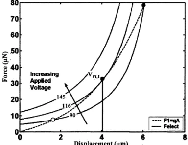
thickness g, = 8 pm, and the upper gap thickness g2= 3.5 pim, (as defined in Figure 2.1 and Figure 2.2). The Young's modulus, E = 160 GPa, the residual stress, -o = 15 MPa, and the beam and electrode width, w = 20 jim. In a plot of force versus displacement, the intersections of Equation 4 or 5 with 6 for a variety of voltages describe the possible solutions to the equations (Figure 2.5). When there are two points of intersection, shown

![Figure 1.12: Plot of displacement versus voltage for prototype near-infrared device using a limited process such that the upper beam segment only moved down 0.6 microns before contact [36].](https://thumb-eu.123doks.com/thumbv2/123doknet/13830355.443249/22.918.275.681.215.477/figure-displacement-voltage-prototype-infrared-limited-process-segment.webp)